HAL Id: cea-01366340
https://hal-cea.archives-ouvertes.fr/cea-01366340
Submitted on 14 Sep 2016
HAL is a multi-disciplinary open access
archive for the deposit and dissemination of
sci-entific research documents, whether they are
pub-lished or not. The documents may come from
teaching and research institutions in France or
abroad, or from public or private research centers.
L’archive ouverte pluridisciplinaire HAL, est
destinée au dépôt et à la diffusion de documents
scientifiques de niveau recherche, publiés ou non,
émanant des établissements d’enseignement et de
recherche français ou étrangers, des laboratoires
publics ou privés.
Local electronic structure and photoelectrochemical
activity of partial chemically etched Ti-doped hematite
Maxime Rioult, Rachid Belkhou, Hélène Magnan, Dana Stanescu, Stefan
Stanescu, Francesco Maccherozzi, Cindy Rountree, Antoine Barbier
To cite this version:
Maxime Rioult, Rachid Belkhou, Hélène Magnan, Dana Stanescu, Stefan Stanescu, et al.. Local
elec-tronic structure and photoelectrochemical activity of partial chemically etched Ti-doped hematite.
Studies in Surface Science and Catalysis, Elsevier, 2015, 641, �10.1016/j.susc.2015.01.002�.
�cea-01366340�
Local electronic structure and photoelectrochemical activity of partial
chemically etched Ti-doped hematite
Maxime Rioult
a,⁎
, Rachid Belkhou
b, Hélène Magnan
a, Dana Stanescu
a, Stefan Stanescu
b,
Francesco Maccherozzi
c, Cindy Rountree
a, Antoine Barbier
aa
Service de Physique de l'Etat Condensé, DSM/IRAMIS/SPEC, CNRS UMR 3680, CEA Saclay, F-91191 Gif-sur-Yvette Cedex, France
b
Synchrotron SOLEIL, L'Orme des Merisiers Saint-Aubin, 91192 Gif-sur-Yvette, France
c
Diamond Light Source, Harwell Campus, Didcot, OX11 0DE Oxforshire, United Kingdom
a b s t r a c t
a r t i c l e i n f o
Available online 10 January 2015 Keywords: Fe2O3 Ti doping PEEM Photoanode Surface etching Photoelectrolysis
The direct conversion of solar light into chemical energy or fuel through photoelectrochemical water splitting is promising as a clean hydrogen production solution. Ti-doped hematite (Ti:α-Fe2O3) is a potential key
photoanode material, which despite its optimal band gap, excellent chemical stability, abundance, non-toxicity and low cost, still has to be improved. Here we give evidence of a drastic improvement of the water splitting performances of Ti-doped hematite photoanodes upon a HCl wet-etching. In addition to the topography investi-gation by atomic force microscopy, a detailed determination of the local electronic structure has been carried out in order to understand the phenomenon and to provide new insights in the understanding of solar water split-ting. Using synchrotron radiation based spectromicroscopy (X-PEEM), we investigated the X-ray absorption spectral features at the L3Fe edge of the as grown surface and of the wet-etched surface on the very same sample
thanks to patterning. We show that HCl wet etching leads to substantial surface modifications of the oxide layer including increased roughness and chemical reduction (presence of Fe2+) without changing the band gap. We
demonstrate that these changes are profitable and correlated to the drastic changes of the photocatalytic activity. © 2015 Elsevier B.V. All rights reserved.
1. Introduction
Within the framework of renewable energy development and solar fuels, an increasing attention is paid to the sun light assisted water split-ting as a clean method for hydrogen production. As a matter of fact, hydrogen is an energy carrier of choice which does not lead to any greenhouse gas production if produced with solar light. If the idea of producing hydrogen using water splitting assisted by solar light is very seductive, it remains unfortunately also very challenging and many material science issues have to be solved. During the process, electron-hole pairs are generated in a semiconductor electrode, upon solar light absorption, and are subsequently used to promote the oxido-reduction reactions of water leading to oxygen production at the photoanode and hydrogen production at the photocathode[1,2].
Since the pioneering discovery of water photoassisted electrolysis using semiconducting TiO2in 1972 by Fujushima and Honda[1], several
materials were investigated as photoanodes[3]where the water oxida-tion occurs (2OH−þ 2hþ→1
2O2þ H2O). Hematite, i.e. theα-Fe2O3iron
oxide, is one of the most promising materials regarding its characteris-tics. It is an n-type semiconductor with a quasi-ideal band gap (~2.2 eV) for solar water splitting applications. Indeed this material is
able to absorb ca. 40% of the solar light spectrum and its theoretical solar-to-hydrogen conversion yield reaches 13%[3]. It is abundant on earth and very stable in aqueous environments, which makes it a serious candidate in the framework of environment friendly energy production[4]. Moreover, the valence band edge of hematite is located below the H2O/O2redox potential which favors the water oxidation
reaction[5]. Unfortunately, hematite has not only advantages. It has been demonstrated that it has poor transport properties[6,7](low con-ductivity and low carrier lifetime) and surface kinetics[8]. Besides this, the conduction band edge ofα-Fe2O3is not well positioned with respect
to the potential of water reduction reaction (2H2O + 2e−→ H2+ 2OH−),
thus an external bias is necessary to promote water splitting[9]. Ti-doping of hematite is a seductive idea to improve bare hematite properties and has been the subject of numerous studies in recent years[7,10–15]. We have recently demonstrated that Ti-doping greatly enhances single crystalline hematitefilms water splitting performances by increasing both electrons and holes mobilities and also the free car-rier concentration by one order of magnitude[10,11]. Surface engineer-ing of hematite has also been a widely explored route over the last few years. Major paths concern the deposition of co-catalysts designed to improve the chemical kinetics (e.g. cobalt oxides)[16,17]or the use of overlayers to passivate surface defects where photogenerated charges can recombine (e.g. alumina)[18]. Surface chemical treatments (e.g. with HF or HCl) are inexpensive experimental processes usually used
⁎ Corresponding author. Tel.: +33 1 69 08 39 23. E-mail address:maxime.rioult@cea.fr(M. Rioult).
http://dx.doi.org/10.1016/j.susc.2015.01.002
0039-6028/© 2015 Elsevier B.V. All rights reserved.
Contents lists available atScienceDirect
Surface Science
for sample preparation. These processes are also commonly used to re-move native and/or amorphous oxide on semiconductors' surfaces (like Si wafer cleaning). In parallel, it has been reported that such wet chem-ical etching can also improve the surface conductivity and semiconduc-tors' photocurrent. For instance, Ziegler et al.[19]reported that a concentrated HCl etching of p-type gallium phosphide removes the na-tive gallium oxide, inducing a 0.2 V reduction of the onset potential. Chernomordik et al.[20]reported that a HF treatment on hematite nanowires removes the amorphous iron oxide phase at the surface of the nanowires, resulting in a single crystalline surface and in a reduction of the onset potential by 0.3 V. Moreover, Basilio et al.[21]reported that a H3PO4crystallographic wet etching on GaN photocathodes (water
re-duction) (i) generated a greater surface area (+14%), (ii) decreased the surface carrier concentration by cleaning up the surface defects and (iii) caused the appearance of stepped edges and etched facets with better photocatalytic activity, resulting in doubling the energy conversion efficiency.
Nonetheless, chemical wet-etching of oxides may induce additional deep morphology and electronic structure changes. In the present work, we examine the effect of HCl etching on the surface of Ti-doped hema-tite epitaxialfilms and the improved photoelectrochemical properties of thesefilms. The films were deposited by atomic oxygen assisted molec-ular beam epitaxy (AO-MBE) on Pt (111) single crystals. AO-MBE allows a high control of the stoichiometry and of the crystalline quality of the thinfilms. Working on oxide epitaxial thin films deposited on single crystals prevents the formation of a native or amorphous oxide phase at the surface that could lower the water splitting performances or mingle characterizations[20]. To study the chemical wet-etching effect on our particular system, we studied Ti-doped hematite thinfilms pat-terned by optical lithography and partially HCl-etched, making possible the simultaneous investigation of as-grown and etched surfaces on the very same sample. Topography and spatial-resolved electronic structure measurements were performed by atomic force microscopy (AFM) and X-ray photoemission electron microscopy (X-PEEM) respectively. Mi-croscopy techniques are tools of choice to investigate the local variation of a particular physical property.
2. Materials and methods
2.1. Sample preparation (deposition, lithography and etching)
Ti-doped hematite layers of 20 nm thickness were deposited on single crystalline Pt (111) substrates using AO-MBE, a technique that makes possible the deposition of epitaxial layers of controlled morphol-ogy, thickness and doping level. The principle and the specificities of this technique were described elsewhere as well as the growth of Ti-doped hematite thinfilms.[10,11,22,23]By UV lithography, we defined on the sample surface micrometric squared (10–50 μm wide) patterns of resist (S1813). After a 15 min annealing at 110 °C on a hot plate the samples were dipped in a bath of 38%-HCl for partial etching and then cleaned with distilled water. The etching time was 5 s for a 2 nm step height. In the end, the morphology of the sample consisted in as-grown Ti-doped hematite patches separated from each other by a partially HCl-etched Ti-doped hematite surface. Detailed morphology data are given in Section 3. The resist was cleaned in acetone followed by an isopropanol bath.
2.2. Crystallographic structure and chemistry
In situ Reflexion High Energy Electron Diffraction (RHEED) patterns were observed and acquired duringfilm growth, in order to monitor the crystal quality and structure of the samples. In situ X-ray Photoemis-sion Spectroscopy (XPS) spectra were systematically recorded just after deposition in order to determine the stoichiometry and the electronic structure of thefilms. More precisely, we recorded Fe2p, Ti2p, O1s core levels and the valence band region using Al Kα radiation. The
doping level in atomic percentage of Ti (at.% Ti) is defined as follows: at. % Ti = I(Ti)/[I(Ti) + I(Fe)], where I(Ti) and I(Fe) are respectively the Ti2p and Fe2p integrated intensities corrected by the corresponding Scofield factors (cross sections). For all studied samples, the measured doping level is 2 at.% (±0.3 at.%).
2.3. Photoelectrochemistry
The photoelectrochemical response of ourfilms was studied using a three electrodes cell described previously[10,11]. All electrochemical measurements were performed at room temperature using a NaOH 0.1 M (pH = 13) solution as electrolyte, a platinum wire as counter elec-trode and an Ag/AgCl elecelec-trode for the potential reference (VAg/AgCl=
+ 0.197 V vs. the standard hydrogen electrode (SHE)). The sample was mounted as anode (working electrode) using a dedicated sample holder that allows the contact only between the hematite surface and the electrolyte. The illumination source was a Newport 1000 W Xe Arc
Lamp with an infrared filter with an incident light flux around
100 mW/cm2(measured with a Newport 1918-R Power Meter).
Poten-tial control and current acquisition between the three electrodes were done using a Princeton Applied Research (PAR) 263A potentiostat controlled by a computer. For current vs. voltage measurements, I(V), the potential was swept from 0 to + 0.8 V vs. Ag/AgCl at a speed of 50 mV/s. The photocurrent is defined as the difference between the current recorded under light and the one without (dark).
2.4. Atomic Force Microscopy (AFM)
We used AFM to compare the surface morphology of our samples before and after HCl-etching. The images were acquired using a Bruker™ FASTSCAN head and Nanoscope V controller. The Bruker's FastScan-B cantilevers utilize a 30μm long triangular silicon nitride cantilever with a force constant of 4 N/m. The silicon tip used to collect the topography measurements had an extremely sharp tip radius of 5 nm.
2.5. X-ray PhotoEmission Electron Microscopy (X-PEEM)
X-PEEM is a full-field X-ray spectromicroscopy technique based on the photoemission process, in the same way as conventional XPS (photon in, electron out). Conventional XPS does not provide spatial information below the tens ofμm scale, while X-PEEM gives simulta-neously spectroscopic and microscopic information at scales that can reach tens of nm at best. The use of synchrotron light as primary incident excitation source enables one to use various incident photon energies, making possible real space-resolved imaging of core levels, valence band or absorption edges spectroscopies. Our X-PEEM experi-ments were carried out on the I06 Nanoscience beamline at the Diamond Light Source (Didcot—UK). Before analysis and in order to remove any surface contaminant due to air exposure, the samples were annealed under an O2atmosphere at a pressure of 10−6mbar
and at a temperature of 300 °C for 1 h. 3. Results and discussion
3.1. Structure and chemistry
The growth behavior of Ti-doped and undoped hematite thinfilms has been described in detail in previous works[10,11,22,23]. Briefly, RHEED patterns with straight diffraction lines corresponding to the hematite surface reciprocal lattice were observed, demonstrating an epitaxial growth. The stoichiometry and the Fe and Ti oxidation states were determined by means of in situ XPS measurements. These measurements were performed just after the thinfilm growth prior to the UV lithography and HCl partial etching. By convention, we consid-ered the O1s line at 530.1 eV as reference for the binding energy[10,11].
We measured binding energies of 711.2 eV for the Fe2p3/2core level and
of 719.2 eV for the typical Fe3 +shake-up satellite. This confirms the
Fe3 +ionic state of iron in all as-grown
films and the absence of any Fe2+species. The Ti2p
3/2line shows a narrow single feature at a binding
energy of 458 eV which corresponds to the binding energy of Ti4+
spe-cies included in the hematite host matrix[10,11]. 3.2. Photoelectrochemical properties
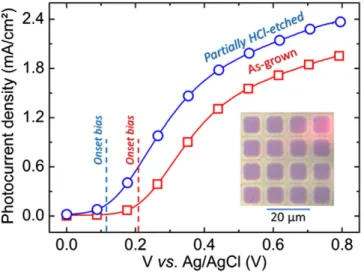
Fig. 1presents the photocurrent density vs. voltage curves for as-grown and 10μm square patterned films (partially HCl-etched, cf. inset inFig. 1, the etching step was about 2 nm). In both cases, only anodic photocurrent appears within the chosen range of potentials. We see that the photocurrent density obtained for the partially HCl-etched sample is at least 25% higher than for the as-grown one for all the bias voltages used. Moreover, for the partial HCl-etched sample the water splitting onset potential is significantly reduced by 0.1 V with respect to the as-grown one.
3.3. Atomic force microscopy
Fig. 2shows the topography AFM picture and the height profile of a film patterned with 10 μm squares (etching step of about 2 nm). From
Fig. 2a (AFM picture) and 2b (height profile), we can see that the overall roughness is increased on the HCl-etched surface. The net result is an in-creased active surface. More precisely, the root mean square (RMS) roughness increases from 1 nm (as-grown surface) to 4.6 nm (partially HCl-etched surface). This roughness increase likely means that the chemical etching is not uniform and that it occurs preferably in the direction perpendicular to the surface along defects of the crystallo-graphic structure like antiphase boundaries[23].
3.4. X-PEEM
The X-PEEM results presented here were obtained on a thinfilm pat-terned with rectangles of various sizes (10μm–50 μm) and a step height of ca. 2 nm. X-PEEM reveals the local electronic structure of iron in our patternedfilms on the as-grown and HCl-etched surfaces within the same region. The Fe L3absorption edge spectra were selectively
record-ed on each area and are depictrecord-ed onFig. 3a for both surface regions. Indeed, the qualitative analysis of these spectra has demonstrated being able to distinguish the electronic configurations of Fe in the differ-ent possible oxide environmdiffer-ents[22]. The crystalfield typical for oxides
splits the L3edge in two characteristic contributions labeled L3Aand L3B.
The shape and relative intensities of these peaks give insight in the va-lence state of the ions and their location in the lattice. The contribution L3Aaround 707.2 eV (resp. L3Baround 708.6 eV), is strengthened in the
presence of Fe2+(resp. Fe3+) ions. This interpretation can be derived
from the simple comparison between reference spectra of Fe3O4(33%
Fe2 +, 67% Fe3 +)[24]andα-Fe
2O3(100% Fe3 +)[22,25](see inset of
Fig. 3a) and has already been used by Droubay et al. in the framework of X-ray absorption microspectroscopy of ilmenite[26]. By comparing the two experimental spectra (Fig. 3a), we observe an increase of the L3Acomponent for the HCl-etched surface. In order to see if this
behav-ior is characteristic of the etched surface we have calculated the ratio R of the intensities of the two peaks of the absorption spectrum (B/A, see
Fig. 3a) on each point of the X-PEEM image. The map of the ratio R is shown inFig. 3c (on a 20μm square) and a Mirror Electron Microscopy (MEM) picture recorded on the same region is shown inFig. 3b.
The MEM mode uses the same setup as X-PEEM, but instead of using photons as excitation source, low energy electrons are used. The MEM images are formed using backscattered low energy electrons and are of high surface morphology sensitivity. As a matter of fact, if the electron energy is not sufficiently high to overcome the surface potential barrier, they are simply reflected by the surface. The contrast in MEM between the as-grown surface and the HCl-etched surface in our case is linked to a work function variation between the as-grown and the etched surfaces, and/or to a difference of roughness, which is consistent with the AFM results. Lines just next to the edges are due to lithography op-tical interference issues. The R mapping (Fig. 3c) follows exactly the morphology with a uniform value in the HCl-etched zone. The black areas in the right center onFig. 3c are due to inhomogeneous incident beam and channel plate saturation. These zones are not visible on the MEM pictures because we use an electron beam as primary source. Moreover R varies from 1.8 on the as-grown surface to 1.6 on the etched one, a value which is intermediate between what is expected for Fe2O3
(≈1.8 for 0% Fe2+) and Fe
3O4(≈1.4 for 33% Fe2+) (see inset ofFig. 3a).
Assuming a linear variation of the R factor with the Fe2+percentage, we can evaluate the amount of Fe2+in the etched region around 15%. Using
the same instrument, we also performed the valence band measure-ment of the two regions. The two spectra were identical even in reso-nant conditions, showing that the Fe2 +introduced by etching does
not reduce the band gap. Patches of sizes different from 20μm exhibited very similar results.
Unlike Ziegler et al.[19]and Chernomordik et al.[20], the HCl etch-ing effect on our hematite layers does not deal with any amorphous structure removal. Indeed the presence of such a structure would have been noticed by RHEED which is sensitive to the crystalline order of the very top surface layer. In our case, partial HCl wet-etching has a sub-stantial effect on the topography of thefilms, but also on their electronic structure and on the iron oxidation state. The roughness increase, consistent with the results reported in reference[21], conjugated with the iron oxide reduction can account for a significant improvement of the photoelectrochemical properties. A roughness increase can easily improve the photoelectrochemical properties thanks to a larger reactive surface. Moreover, as in Ref.[21], we can reasonably assume that the chemical etching is crystalline surface plane dependent. Hence, the pure (0001) hematite surface may make appear upon etching crystal-line planes of higher Miller indexes, which may have better photocata-lytic activity than the basal hexagonal one. Indeed, there is a strong anisotropic conductivity in hematite, the conductivity being 4 times higher perpendicular to the (0001) direction than along it[5]. This phe-nomenon has also been observed in the case of the thoroughly-studied anatase TiO2photoanode material, where water is preferably adsorbed
on (001) facets than on (101) facets[27]. Moreover, the presence of Fe2+can also explain the water splitting improvement because of an
in-creased carrier mobility[28]. Interestingly, the introduction of Fe2 + with HCl etching occurs without changing the band gap, avoiding any alteration of the semiconducting properties of ourfilms.
Fig. 1. Photocurrent density vs. voltage curves for a 2 at.% Ti-doped hematite 20 nmfilm: as-grown ( ), and partially HCl-etched (patterned by UV lithography) ( ). The inset shows the used lithography pattern (10μm squares). Bright zones (resp. dark) correspond to the etched surface (resp. as-grown).
4. Conclusions
The effect of a partial etching by hydrochloric acid on the surface topography and on the electronic structure was investigated by atomic force microscopy and X-ray photoelectron microscopy respectively. It was found that on the one hand HCl etching increases the overall rough-ness of the surface, providing a higher number of catalytic sites. On the other hand, the etched oxide is locally reduced, as it is shown by the presence of Fe2+ions. These changes in the material properties result
in a substantial improvement of the water splitting performances, in
particular a significant reduction of the onset potential. Those results provide new insights on the parameters governing the hematite poten-tial for environment friendly hydrogen production.
Author contributions
The manuscript was written through contributions of all authors. All authors have given approval to thefinal version of the manuscript. Acknowledgments
This work was funded by the CEA project DSM-Energie Hemaphoto and supported in part by Triangle de la Physique and Ile-de-France (C'Nano and ISC-PIF) under the IMAFMP grants.
References
[1] A. Fujishima, K. Honda, Nature 238 (1972) 37.
[2] M. Grätzel, Nature 414 (2001) 338.
[3] R. Van de Krol, Y. Liang, J. Schoonman, J. Mater. Chem. 18 (2008) 2311.
[4] K. Sivula, F. Le Formal, M. Grätzel, ChemSusChem 4 (2011) 432.
[5] A. Kay, I. Cesar, M. Grätzel, J. Am. Chem. Soc. 128 (2006) 15714.
[6] B. Zhao, T.C. Kaspar, T.C. Droubay, J. McCloy, M.E. Bowden, V. Shutthanandan, S.M. Heald, S.A. Chambers, Phys. Rev. B 84 (2011) 245325/1.
[7] J.A. Glasscock, P.R.F. Barnes, I.C. Plumb, N. Savvides, J. Phys. Chem. C 111 (2007) 16477.
[8] L. Badia-Bou, E. Mas-Marza, P. Rodenas, E.M. Barea, F. Fabregat-Santiago, S. Gimenez, E. Peris, J. Bisquert, J. Phys. Chem. C 117 (2013) 3826.
[9] S.D. Tilley, M. Cornuz, K. Sivula, M. Grätzel, Angew. Chem. Int. Ed. 49 (2010) 6405.
[10] M. Rioult, H. Magnan, D. Stanescu, A. Barbier, J. Phys. Chem. C 118 (2014) 3007.
[11] H. Magnan, D. Stanescu, M. Rioult, E. Fonda, A. Barbier, Appl. Phys. Lett. 101 (2012) 133908/1.
[12] O. Zandi, B.M. Klahr, T.W. Hamann, Energy Environ. Sci. 6 (2013) 634.
[13] J. Deng, J. Zhong, A. Pu, D. Zhang, M. Li, X. Sun, J. Appl. Phys. 112 (2012) 084312/1.
[14] H. Tang, M.A. Matin, H. Wang, T. Deutsch, M. Al-Jassim, J. Turner, Y. Yan, J. Appl. Phys. 110 (2011) 123511/1.
[15] M. Zhang, W. Luo, Z. Li, T. Yu, Z. Zou, Appl. Phys. Lett. 97 (2010) 042105/1.
[16] L. Xi, P.D. Tran, S.Y. Chiam, P.S. Bassi, W.F. Mak, H.K. Mulmudi, S.K. Batabyal, J. Barber, J.S.C. Loo, L.H. Wong, J. Phys. Chem. C 116 (2012) 13884.
[17] S. Riha, B.M. Klahr, E.C. Tyo, S. Seifert, S. Vajda, M.J. Pellin, T.W. Hamann, A.B.F. Martinson, ACS Nano 7 (2013) 2396.
[18] F. Le Formal, K. Sivula, M. Grätzel, J. Phys. Chem. C 116 (2012) 26707.
[19] J. Ziegler, D. Fertig, B. Kaiser, W. Jaegermann, Energy Procedia 22 (2012) 108.
[20] B.D. Chernomordik, H.B. Russell, U. Cvelbar, J.B. Jasinski, V. Kumar, T. Deutsch, M.K. Sunkara, Nanotechnology 23 (2012) 194009/1.
[21]A.M. Basilio, Y.K. Hsu, W.H. Tu, C.H. Yen, G.M. Hsu, O. Chyan, Y. Chyan, J.S. Hwang, Y.T. Chen, L.C. Chen, K.H. Chen, J. Mater. Chem. 20 (2010) 8118.
[22]A. Barbier, R. Belkhou, P. Oehresser, M. Gautier-Soyer, O. Bezencenet, M. Mulazzi, M.J. Guittet, J.B. Moussy, Phys. Rev. B 72 (2005) 245423/1.
[23] A. Barbier, O. Bezencenet, C. Mocuta, J.B. Moussy, H. Magnan, N. Jedrecy, M.J. Guittet, M. Gautier-Soyer, Mater. Sci. Eng. B 144 (2007) 19.
[24]H. Magnan, P. Le Fèvre, D. Chandesris, P. Krüger, S. Bourgeois, B. Domenichini, A. Verdini, L. Floreano, A. Morgante, Phys. Rev. B 81 (2010) 085121/1.
[25] F. Jiménez-Villacorta, C. Prieto, Y. Huttel, N.D. Telling, G. van der Laan, Phys. Rev. B 84 (2011) 172404/1.
[26] T. Droubay, G. Mursky, B.P. Tonner, J. Electron. Spectrosc. Relat. Phenom. 84 (1997) 159.
[27] W.G. Fang, X.Q. Gong, H.G. Yang, J. Phys. Chem. Lett. 2 (2011) 725.
[28] P.H. Borse, H. Jun, S.H. Choi, S.J. Hong, J.S. Lee, Appl. Phys. Lett. 93 (2008) 173103/1.
Fig. 2. (a) 2D topography AFM picture of a patterned 2 at.% Ti:Fe2O3(20 nm thickness, 2 nm step height). (b) Height profile along the white dashed line (gray curve).
Fig. 3. (a) Fe L3absorption edge for the as-grown surface (red solid line) and the etched
surface (blue dashed line). Orange items show the positions of the L3Aand L3B
contribu-tions, as well as the R coefficient graphic determination. The inset shows experimental spectra of reference Fe2O3(gray solid line) and Fe3O4(black solid line)films. (b) MEM