HAL Id: hal-01797591
https://hal.archives-ouvertes.fr/hal-01797591
Submitted on 2 Jul 2020HAL is a multi-disciplinary open access archive for the deposit and dissemination of sci-entific research documents, whether they are pub-lished or not. The documents may come from teaching and research institutions in France or abroad, or from public or private research centers.
L’archive ouverte pluridisciplinaire HAL, est destinée au dépôt et à la diffusion de documents scientifiques de niveau recherche, publiés ou non, émanant des établissements d’enseignement et de recherche français ou étrangers, des laboratoires publics ou privés.
Coupled HgSe colloidal quantum wells through a
tunable barrier: a strategy to uncouple optical and
transport band gap
Eva Izquierdo, Marion Dufour, Audrey Chu, Clément Livache, Bertille
Martinez, Dylan Amelot, Gilles Patriarche, Nicolas Lequeux, Emmanuel
Lhuillier, Sandrine Ithurria
To cite this version:
Eva Izquierdo, Marion Dufour, Audrey Chu, Clément Livache, Bertille Martinez, et al.. Coupled HgSe colloidal quantum wells through a tunable barrier: a strategy to uncouple optical and transport band gap. Chemistry of Materials, American Chemical Society, 2018, �10.1021/acs.chemmater.8b01028�. �hal-01797591�
Coupled HgSe colloidal quantum wells through a tunable barrier: a strategy to uncouple optical and transport band gap
Eva Izquierdo1,2, Marion Dufour1,2, Audrey Chu1,2,3, Clément Livache1,2,3, Bertille Martinez1,2,3, Dylan Amelot3, Gilles
Patriarche4, Nicolas Lequeux1,2, Emmanuel Lhuillier3, Sandrine Ithurria1,2* 1 LPEM, ESPCI Paris, PSL Research University, CNRS, 75005 Paris, France
2 Sorbonne Université, CNRS, LPEM, 75005 Paris, France
3 Sorbonne Université, CNRS, Institut des NanoSciences de Paris, INSP, F-75005 Paris, France
4 Centre de Nanosciences et de Nanotechnologies, CNRS - Université Paris Sud, Université Paris Saclay, route de
Nozay, 91460 Marcoussis
Abstract: Among semiconductor nanocrystals (NCs), 2D nanoplatelets (NPLs) are a special class of nanomaterials with well controlled optical features. So far most of the efforts have been focused on wide band gap materials such as cadmium chalcogenide semiconductors. However, optical absorption can be pushed toward the Infra-Red (IR) range using narrow band gap materials such as mercury chalcogenides. Here we demonstrate the feasibility of a core/shell structure made of a CdSe core with two HgSe external wells. We demonstrate that the optical spectrum of the heterostructure is set by the HgSe wells and this, despite the quasi type II band alignment which makes the band edge energy independent of the inner core thickness. On the other hand, these core/shell NPLs behave, from a transport point of view, as a wide band gap material. We demonstrate that the introduction of a wide band gap CdSe core makes the material less conductive and with a larger photoresponse. Hence the heterostructure presents an effective electric band gap wider than the optical band gap. This strategy will be of utmost interest to design infrared effective colloidal materials for which the reduction of the carrier density and the associated dark current is a critical property.
Keywords : Nanoplatelets, Heterostructure, Narrow band gap materials, Band engineering. To whom correspondence should be sent: [email protected]
INTRODUCTION
Colloidal quantum dots have generated a large interest because of their tunable optical feature from UV to THz.1 In
addition their bright luminescence make them appealing candidates for a broad variety of applications spanning from single photon source2, to light emitter for displays or even for laser3,4,5. In all these applications, the wavefunction
engineering remains at a very basic level and mostly consists in band gap tunability thanks to quantum confinement. In this sense, colloidal heterostructure remains far below the maturity that is achieved with epitaxially grown heterostructure of III-V semiconductors. Quantum well infrared photodetectors6,7 and quantum cascade structure used
for detection8,9 and lasing10 are certainly the state of the art of wavefunction engineering. In such heterostructure,
quantum states are coupled using phonon10 or other scattering mechanisms11. A key step to the wavefunction engineering
into colloidal systems was the introduction of wide band gap type I heterostructure to boost the photoluminescence efficiency12. Some other improvements were made by growing complex colloidal heterostructures with multi shell13 or
anisotropic shell14,15. Type II heterostructures have also been proposed16,17 for the design of long living exciton: in such
system, one high work function material is combined with a lower work function material to obtain a colloidal p-n junction. In such material, one material confines the electron and the other the hole. Finally, one of the most (conceptually) complex attempt for wavefunction engineering in colloidal material was proposed by Cragg et al18 who
suggested that gradient interface heterostructures should be used to reduce Auger effect. Here, we try to bring wavefunction engineering into colloidal material to the next level and demonstrate that core/shell structure made of a CdSe core surrounded by HgSe wells can be grown and present transport properties which can be tuned independently from their optical features. In other words, we build an heterostructure for which the optical band gap is not the electrical band gap.
This result is of utmost importance for narrow band gap materials dedicated to infrared (IR) detection. When it comes to detection in the IR range of the electromagnetic spectrum, transition energies are small and phonon activated carriers compete with optical excitation. As a result, the noise, rather than the signal itself becomes the main challenge. The noise magnitude is tightly bonded to the amount of dark current and thus to the dark carrier density. Designing a material for which the transport band gap is larger than the optical band gap is very promising to obtain near and mid IR devices based on colloidal materials.19
In this paper, we demonstrate the growth of 2D heterostructures made of a CdSe core surrounded by a shell of HgSe. Weller group has already reported quantum well structures of spherical Cd/Hg/CdE (E = S or Te) nanocrystals20,21. On
these systems, it has been shown that the transition energy can be tuned by the core diameter of CdE (E = S or Te), the thickness of the well (mercury layer) and the thickness of the external shell. After the cation exchange on CdE quantum dots by mercury, the nanocrystals don’t present any fluorescence. By adding Cd2+ ions on Cd/HgE structures, the
fluorescence significantly increases by charge carriers confinement in the HgE layer. This observation was confirmed by a theoretical approach on the probability of the presence of electrons and holes in the nanoparticles22.
CdSe 2D nanoplatelets (NPLs) are a special class of nanocrystals (NCs)23,24, which present no inhomogeneous
broadening. A thickness, defined at the atomic scale, leads to narrower excitonic features compared to 0D spherical equivalent. Recently, Izquierdo et al25 showed, that such narrow excitonic features could be extended to near-IR range
by synthesizing HgTe and HgSe NPLs. The latter are obtained via a Hg2+ cation exchange procedure conducted on thin
CdSe and CdTe NPLs. So far only homomaterials of mercury chalcogenides have been reported. Here we extend the method and achieve a partial cation exchange on thicker NPLs. We bring evidence of a CdSe core embedded between two HgSe quantum wells. The electronic properties and transport properties of the formed heterostructures are then discussed. Finally, we finish the discussion by addressing the carrier relaxation dynamics using transient photocurrent measurements.
EXPERIMENTAL METHODS Chemicals
Se powder (Sigma-Aldrich), Mercury acetate (Hg(Ac)2) (Aldrich, > 99.0%), Cadmium acetate (Cd(Ac)2) (STREM, 98
%), Cadmium oxide (CdO) (STREM, 99.99 %), Myristic acid (Fluka, > 98 %), Oleylamine (Acros, 80-90 %), Tri-butylphosphine (TBP) (Cytec), Oleic acid (OA) (Aldrich, 90%), Octadecene (ODE) (Aldrich, 90 %), n-Hexane (VWR, 99 %), Toluene (VWR, 99.8 %), Ethanol (VWR, 95-97 %), Methanol (Carlo Erba, 99.9 %), N-methylformamide (NMF) (Carlo Erba, 99 %), LiClO4 (Aldrich, 98 %), Polyethylene glycol MW = 6x10³ g.mol-1 (PEG 6k) (Fluka).
Precursors
Cadmium myristate: In a 100 mL three neck flask, 2.56 g of CdO and 11 g of myristic acid are degassed under vacuum
for 30 minutes at 70°C. Under argon flow, the mixture is heated up to 200°C for 30 minutes until the solution becomes colorless. Then, 50 mL of MeOH is added between 60°C and 70°C in order to solubilize the excess of myristic acid. The mixture is stirred for 30 minutes. At the end, the cadmium myristate is precipitated by using centrifuge tube through the addition of MeOH. The washing procedure is repeated at least three times. The cadmium myristate is dried overnight under vacuum.
TOPSe (1M): In the glove box, 1.58 g of Se powder are mixed with 20 mL of trioctylphosphine and let stir until complete
dissolution of Se in TOP.
Selenide solution (0.1 M): In the glove box, 40 mg of NaBH4 are dissolved in 0.5 mL of NMF and 0.5 mL of ethanol.
Then 24 mg of selenium powder are added. NaBH4 reduces the selenium powder in SeNa2 with the formation of H2.
After ten minutes the reaction should be complete and the mixture should turn colorless. Nanocrystals synthesis
Synthesis of 3 MLs CdSe NPLs: In a three neck flask, 240 mg of Cd(Ac)2 and 10 mL of ODE are degassed under vacuum
for 10 min at room temperature. Under argon flow, the mixture is heated up to 200 °C. A solution of 400 µL of TOPSe at 1M, 200 µL of OA and 3.75 mL of ODE is injected drop by drop (5 mL.h-1). After the injection, the mixture is cooled
down and precipitated with a mixture of 10 mL of hexane and 5 mL of ethanol. The NPLs are suspended in 10 mL of hexane.
Synthesis of 4 MLs CdSe NPLs: In a 50 mL three neck flask 340 mg of Cd(myristate)2, 24 mg of Se and 25 mL of ODE
are degassed for 30 minutes at room temperature. Under Argon flow, the temperature is raised to 240 °C. When the mixture reaches 200 °C, 100 mg of Cd(Ac)2are introduced. The reaction is stopped after 10 minutes at 240 °C. The
NPLs are precipitated through the addition of a mixture of 30 mL of hexane and 30 mL of ethanol. The NPLs are suspended in 10 mL of hexane.
CdSe growth by c-ALD: 4 mL of 3 MLs NPLs solution is precipitated with ethanol and suspended in 2 mL of hexane.
In the glove box, 20 µL TBP, 20 µL of EtOH and 150 µL of the sodium selenide solution are added to the NPLs. The solution is vigorously stirred up to the complete precipitation of the NPLs and a color change from yellow to orange is observed. Then 2 mL of NMF are added to resuspend the precipitated NPLs. The NPLs should be stable in NMF, if not sodium selenide solution and TBP should be added to the biphasic medium. The solution is taken out of the glove box and the hexane is removed. The NPLs in NMF are first washed with a mixture of 3 mL of hexane, 20 µL of TBP and 20 µL of EtOH and second with 3 mL of hexane and 20 µL of EtOH. To grow the half layer of Cd, 200 µL of a solution of Cd(Ac)2 in NMF at 0.1 M is added. The solution is vigorously stirred until it becomes red. Then the NPLs are
transferred back to hexane thanks to oleylamine. The addition of MeOH facilitates the phase separation. Finally, the NPLs are precipitated and suspended in 6 mL of ODE. The crystallinity of the NPLs is improved with an annealing step. In 25 mL three neck flask, the NPLs in ODE, 50 mg of Cd(Ac)2, 70 µL of oleic acid and 70 µL of TBP are degassed for
20 minutes at room temperature. Under argon flow, the mixture is heated up at 230°C for 20-25 minutes until the refinement of the optical features. Finally, the NPLs are precipitated with EtOH and suspended in 8 mL of hexane. The same process is reproduced for each additional layer.
Cation exchange
3MLs HgSe NPLs: In a flask, 2 mL of toluene, 20 µL of 3 MLs CdSe nanoplatelets (OD = 1 at 400 nm) and 3 µL of
oleylamine are introduced. Then 15 µL of a freshly prepared solution at 0.08 M of Hg(Ac)2 in MeOH is introduced at
room temperature (the ratio Cd:Hg is 1:1.2). The cation exchange is monitored by absorption spectroscopy (Figure S1 a.). When the first exciton has reached 735 nm, the nanoplatelets are precipitated and resuspended in hexane. Regarding
the lateral sizes, the nanoplatelets precipitated without addition of a polar solvent. On TEM images (Figure S1 b. and c.), it can be observed that the NPLs morphology is preserved during the exchange process.
Core-shell CdSe/HgSe NPLs: In a typical reaction, 3 µL of OAm and 15 µL of a freshly prepared solution at 0.08 M of
Hg(Ac)2 in MeOH are introduced at room temperature in CdSe NPLs solution suspended in 2 mL of toluene. The cation
exchange occurred with a typical time scale of 20 minutes, see Figure S2. Absorption at short wavelength gives some information on the amount and the composition of materials in solution26. After c-ALD growing, there are two more
planes of Cd and Se on the NPLs, while keeping the lateral sizes unchanged. To have the same concentration of NPLs, if the starting 3 MLs CdSe NPLs solution (7 atomic planes) have an optical density of 1 at 400 nm, the OD of 5 MLs CdSe NPLs (11 atomic planes) should be 1.57 at 400 nm. Consequently with the same reasoning, the OD of 7 MLs (9 MLs or 11 MLs) CdSe NPLs solution should be 2.14 (respectively 2.71 or 3.28). For each population, the ratio of mercury and NPLs is identical. Consequently, the amount of Cd exchanged is the same, corresponding to 2 planes of cations on the external sizes of NPLs.
DISCUSSION
II-VI NPLs materials23 present optical features free of inhomogeneous broadening which results from roughness free
atomic surfaces in the confined direction. While for cadmium based semiconductors, large efforts have been dedicated to the growth understanding27,28, the growth of heterostructures with various materials29 and spatial organizations
(core/shell30 and core/crown31), far less effort has been dedicated to narrower band gap materials. Recently, our group
proposed to use cation exchange to indirectly synthesize HgTe and HgSe NPLs25. The procedure leads to a complete
cation exchange and to pure mercury chalcogenides NPLs free of initial cadmium (ie final objects are neither alloys, nor gradients). As for cadmium chalcogenide NPLs, these nanoparticles crystallize in a zinc blende structure with the thickness along the [001] direction.
The softness of mercury chalcogenides and their ability to aggregate make the growth of heterostructure difficult and only few reports exist22,32,33,34,35. Here, we proceed in two steps to synthesize HgSe/CdSe/HgSe heterostructures. In a
first step, we synthesize CdSe NPLs with variable thicknesses from 3 monolayers (MLs) to 11 MLs36. Note that N ML
NPLs refer to nanoparticles with N layers of anions and N+1 layers of cations in the thickness (2N+1 layers in total). The additional cadmium plane comes from the cadmium rich top and bottom faces. In a second step, these CdSe NPLs are exposed at room temperature to a precursor of mercury which allows proceeding to the partial cation exchange. In the first step, we preliminarily synthesize 3 and 4 ML CdSe NPLs using already established procedures37, see Figure
1a and b. Then we use the colloidal Atomic Layer Deposition30 (c-ALD) procedure to further increase the thickness of
the NPLs and obtain NPLs with up to 11 MLs, see Figure 1c and d. The c-ALD procedure is well established to grow metal sulfide semiconductors thanks to the easy handling of sulfide precursors. A contrario, the growth of selenide based semiconductors is more sensitive, due to the easy oxidation of Se2- in polyselenide. Thus, the growth of the Se layer was
done by using fresh sodium selenide Na2Se solution obtained from the reduction of Se powder in presence of a strong
reducing agent (NaBH4)38. These selenide anions allow the transfer of NPLs in the polar N-methylformamide. Then, the
additional Cd layer is grown through reacting the selenium rich NPLs with cadmium acetate. The NPLs are transferred back in a non-polar solvent with addition of oleic acid. Starting from N ML CdSe NPLs, a c-ALD process leads to N+2 ML CdSe NPLs.
The CdSe NPLs suspended in a non-polar solvent are exposed to mercury acetate complexed with oleylamine. By doing so, the cation exchange is only complete for 3 ML NPLs (see Supporting Information Figure S1). For all thicker NPLs (see Supporting Information Figure S2 and S3), we observe using energy dispersive X-ray spectrometry (EDX) and Rutherford Backscattering Spectrometry that the final NPLs still include cadmium (see Supporting Information Table S1 and S2, Figure S8). We also notice that for all these populations, the ratio of Hg/Cd is consistent with the amount expected for 4 planes of Hg. Hg cannot diffuse up to the center of the particle and it only diffuses over two layers on the surface of the NPLs. This hypothesis is further confirmed using high angle annular dark field (HAADF) scanning transmission electron microscopy (STEM) imaging, with a high Z contrast imaging, see Figure 1g. We clearly see two bright layers on the external planes of the NPLs due to Hg, while the inner part of the NPLs is less intense due to the lower electronic density of Cd (see Supporting Information Figure S5). Thus, it is possible to exclude the possibility to have either a gradient or an homogeneous HgCdSe alloy. The core/shell structure will be further confirmed by other techniques such as X-ray diffraction (XRD) and optical measurements.
Figure 1 (a.) Scheme of a 4ML thin CdSe NPL and (b.) TEM image of 4 ML thin CdSe NPLs. (c.) Scheme of a 10ML thick CdSe NPL and (d.) TEM image of 10ML thick CdSe NPLs. (e.) Scheme of a 10ML HgSe/CdSe/HgSe heterostructure. (f.) TEM and (g.) high resolution TEM in dark filed mode of a 10ML HgSe/CdSe/HgSe heterostructure.
Such uncomplete cation exchange has already been observed in other systems such as PbS/CdS39 and CdTe/HgTe40–42.
It is more likely to happen when the host and replacing cations have the same level of oxidation and comparable sizes. In addition CdSe and HgSe share the same zinc blende crystal structure with really close lattice parameters, aCdSe= 0.605
nm and aHgSe= 0.608 nm (See Figure S6 for X Ray Diffraction (XRD)). Moreover, the mercury is larger than cadmium,
which leaves less room for the interstitial insertion. In NPLs the top and bottom facets, which can represent ≈95% of the total surface, are cation rich and stabilized by carboxylates. In order to induce cation exchange, it is necessary to create local cation vacancies on these surfaces. Here, the introduction of oleylamine and methanol which have a good affinity for cations, can remove few cadmium atoms from the surface. Then, as it has been proposed by Hens and co-workers39 for cadmium in PbS NCs, the mercury can diffuse over few layers. This low diffusivity has also been observed
in spherical CdTe NCs and was estimated at the submonolayer level42. In NPLs, the top and bottom facets are,
chemically, strictly equivalent, hence have the same reactivity. Here, the mercury diffusion is limited to exactly 2 planes in the [001] direction of the thickness. Thus a total of 4 planes of cadmium are exchanged and the diffusion of mercury is limited to 4Å.
The XRD patterns show that after exchange (see Figure S6), the zinc blende crystalline structure is not affected. CdSe core NPLs present XRD patterns shifted compared to their theoretical positions. This is explained by the surface ligands which induce strain in the crystals. Oleate ligands lead to an extension of the lattice parameter in the lateral dimensions and a contraction in the thickness.43 As the thickness of the CdSe NPLs increases, the diffraction peaks are approaching
their theoretical positions. After cation exchange, the peaks end up to positions close to those expected for the bulk. Since HgSe and CdSe have the same lattice parameters, the incorporation of HgSe in or on CdSe should not bring new stress in the material. Nevertheless, CdSe and HgSe have different bulk moduli of around 60 GPa44 and 50 GPa45, which
means that the “softness” of HgSe allows absorbing ligands stress. Thus the shift observed after cation exchange may originate from the nature of the external layer at the interface between the solid and the ligands. These results are also pledging for a core/shell structure, here after noted HgSe/CdSe/HgSe NPLs. Here the DRX, EDX data and TEM suggest that the interface between the core and the shell is abrupt. This is further confirmed with the optical properties.
The electronic structure of the NPLs can be investigated thanks to absorption spectroscopy. In Figure 2a, we plot the absorption spectra for each NPL thickness before and after Hg cation exchange. For the CdSe NPLs (highlighted by a green band in Figure 2a), we see a clear shift of the excitonic feature from 460 nm for the 3 ML NPLs to 666 nm for the 11 ML NPLs, as the NPL thickness increases in accordance with a decrease of the (dieletric) confinement. In Figure 2b, the energies of the heavy hole and light hole to electron transitions are plotted as function of the thickness given in number of MLs for CdSe NPLs (green dots). For the HgSe/CdSe/HgSe heterostructures, on the other hand, the absorption spectra show that the band edge energy is almost unchanged regardless of the thickness of the CdSe core barrier and appears around 750 nm (1.65 eV) with two excitonic peaks (highlighted with a red band in Figure 2a and Figure 2b). The absorption spectra of the HgSe/CdSe/HgSe heterostructures also reveal a second feature (the blue band in Figure 2a) at higher energy which depends on the core thickness. The energy of this feature reasonably fits the band edge energy of CdSe NPLs for which 3 MLs would have been removed, see Figure 2b. Indeed, when 10 ML CdSe NPLs are exchanged with mercury, the obtained NPLs are, regarding our notation, HgSe(1ML)/Se/CdSe(6MLs)/Se/HgSe(1ML). The selenium planes which separate the CdSe and HgSe quantum well belong to both materials. Thus the CdSe core is equivalent to 7 ML CdSe NPLs (total of 15 planes: 7 planes of cadmium alternated with 8 planes of selenium) while the HgSe shell is equivalent to 1.5 ML HgSe quantum well (2 planes of mercury alternated with 2 planes of selenium), see Figure 1e and Figure 2b. Hereafter in this article, the exchanged NPLs coming from the N MLs CdSe will be named N MLs HgSe/CdSe/HgSe NPLs.
Figure 2 (a.) Absorption spectra of the CdSe NPLs before (black curve) and after cation exchange (red curve) for different thicknesses of the initial objects. The green band represents the variation of the first two transitions in CdSe NPLs. The red band (resp. blue band) represents the transitions at lower energies (resp. higher energies) in the exchanged NPLs (b.) Energies of the two band edge features (red peaks) and from the bluer features (labelled blue peaks) for exchanged NPLs and from the two first exciton transitions for the CdSe NPLs. The black arrows show the equivalent CdSe core quantum well after cation exchange. Energy band profile and associated wavefunction for a HgSe/CdSe/HgSe heterostructure with 6 MLs thickness (c.) and 11 MLs (d.).
To further elucidate the observed spectra, the energy and alignment of the formed heterostructure needs to be discussed. HgSe as bulk material is a semimetal (ie there is no band gap), CdSe is a semiconductor with a 1.7 eV band gap. From photoemission, it was determined that the valence band offset between HgSe and CdSe is 0.6 eV.46 The energy band
profile of the formed heterostructure is typically given for two NPLs thicknesses in Figure 2c and 2d. We then solve numerically the 1D time independent Schrödinger equation, see Supporting Information for details, to obtain the electronic spectrum of the formed heterostructure. The method is basic since it neglects mirror charge effect47, dielectric
confinement48,49 and band non parabolicity but useful to obtain qualitative dependence due to confinement. Our
simulation predicts a quasi-type II band alignment, with a hole confined in HgSe and 1Se electron state delocalized over the heterostructure, see Figure 2c. and d. At first sight, the delocalized character of the electron wavefunction might appear in contradiction with the lack of dependence of the interband energy with the size of the CdSe barrier. However, the 1Se state is almost resonant with the top of the CdSe bulk band gap (100-200 meV above) which provides to the 1Se state only a little of the CdSe character. As a result, the electronic state is only poorly delocalized over the whole heterostructure and energetically behaves as if the electronic state was confined in HgSe.
Finally the blue structure observed in the HgSe/CdSe/HgSe heterostructure spectrum is the result of the 1Dh to 1Se transition, see blue arrow on Figure 2c and 2d. Indeed the 1Dh state has a maximum density of presence in the CdSe barrier, which provides this transition a strong CdSe character and explains the good matching between the energy of the blue features of the heterostructure with the transitions of 3 ML thinner CdSe NPLs (see black arrows in Figure 2b). At this point, we have designed an heterostructure, with a band edge energy marginally (only the broadening) affected by the presence and size of the central CdSe tunnel barrier. In the following, we demonstrate that this barrier is nevertheless playing a central role onto the electronic properties of thin film of NPLs.
2 4 6 8 10 12 1,5 1.8 2,1 2,4 2,7 3,0 E n e rg y (e V ) Number of MLs 400 500 600 700 800 O p tic a lD e n si ty (a .u .) Wavelength (nm) 3 MLs 4 MLs 5 MLs 6 MLs 7 MLs 8 MLs 9 MLs 10 MLs 11 MLs Energy (eV) 0 1 2 -1 -2 z (nm) vacuum vacuum 0 1 2 -1 -2vacuum vacuum 6 MLs 11 MLs a. b. c. d. Energy (eV) z (nm) Red - 1st trans Red - 2nd trans Blue - 1st trans Blue - 2nd trans CdSe - 1st trans CdSe - 2nd trans CdSe NPLs HgSe/CdSe/HgSe NPLs - 3MLs 1 2 3 4 1 2 3 4 5 1Se 1Se 1Pe 1Sh 1Ph 1Sh 1Ph 1Dh 1Dh
To evidence that, we investigate the transport properties of an array of HgSe and HgSe/CdSe/HgSe NPLs. To obtain conductive film of NPLs we first performed a ligand exchange from acetate/oleylamine insulating ligands to short S2-
anions50 through a well-established phase transfer procedure. Once deposited on electrodes, the NPL films are used as
the channel of an ion gel gated electrolytic transistor51. This method combines several advantages such as air operability,
gating of thick film and low bias operation due to the large electrolyte capacitance. A scheme of the setup is shown in Figure 3a.
Figure 3 (a.) Scheme of an electrolytic transistor where a thin film of NPLs is used as channnel. (b.) Transfer curve (drain current vs gate bias) for HgSe/CdSe/HgSe heterostructures of various thicknesses. As the conductivity of the sample strongly changes, the curves have been normalized to better illustrate the shift of the threshold voltage. Non normalized data are given in Figure S9 (c.) Threshold voltage for transistor made of HgSe/CdSe/HgSe heterostructures as a function of the thickness of the NPL. (d.) I-V curve of a film of 3ML HgSe NPLs measured at room temperature under dark condition and under illumination (λ=532 nm- P=0.13 mW). (e.) I-V curve of a film of 11ML HgSe/CdSe/HgSe heterostructures measured at room temperature under dark condition and under illumination (λ=532 nm- P=0.13 mW).
The transfer curves of the NPL films are given in Figure 3b and S9. All NPLs present a n-type character, with a rise of the conductance upon electron injection. However the threshold voltage strongly raises while the CdSe barrier thickness is increasing, see Figure 3c. Only the pure HgSe NPLs present a negative threshold voltage, which is the expected behavior for degenerately doped semiconductor (ie when the Fermi level is, in or close, to the conduction band). Once a CdSe barrier is present, the threshold voltage becomes positive, which is typical behavior for wide band gap barrier with a Fermi level deep into the band gap. This reduction of doping is strongly impacting the film conductance and we observe a reduction of the conductance by five orders of magnitude as the NPLs thickness increases from 3 MLs to 11 MLs, see Figure 3d and e. Assuming an Arrhenius law for the temperature scaling of the conductance
(
E
k
T
)
G
exp −
a/
b , we obtain a difference between the electrical gap and the transport gap given by(
HgSe
CdSe
)
E
(
HgSe
)
k
T
G
(
HgSe
) (
G
HgSe
CdSe
)
E
a/
=
a+
bln
/
/
. This corresponds to an increase of the electricalgap of 300 meV with respect to the optical gap. The effective increase of the band gap also dramatically impacts the NPLs -0,4 -0,2 0,0 0,2 0,4 -4x10- 4 -2x10- 4 0 2x10- 4 4x10- 4 Glight/Gdark= 1 Dark Light
I
DS(A
)
V
DS(V)
-1,0 -0,5 0,0 0,5 1,0 -4x10- 7 -2x10- 7 0 2x10- 7 4x10- 7 DarkLight Glight/Gdark= 51I
DS(A
)
V
DS(V)
-2 -1 0 1 2 3 MLs 5 MLs 7 MLs 9 MLs 11 MLsC
u
rr
e
n
t
(a
.u
.)
V
GS(V)
2 4 6 8 10 12 -3 -2 -1 0 1T
h
re
sh
o
ld
(V
)
MLs number
SiO2 Source Drain Gate Electrolyte b. c. d. e. a. 3MLs HgSe 11MLs HgSe/CdSe/HgSephotoconductive properties of the film. Thin HgSe NPLs are quasi non photoresponsive, see Figure 3d. On the other hand, in presence of a CdSe barrier, a clear photoconductance signal is measured (see Figure 3e), with an increase of the conductance by a factor 50 under illumination. While the presence of the barrier was leading to marginal effect on the absorption spectrum, its impact on transport is drastic. By finely controlling the doping of the system, through the CdSe barrier, it switches from narrow band gap semiconductor behavior, with strong conductance and weak photoresponse to a typical behavior expected for wide band gap material. In other words, we have built a system whose optical properties are set by the narrow band gap HgSe layers, but behaves as the wide band gap CdSe core from a transport point of view. One key question is then to determine if these properties result from the heterostructure or the presence of a mixture of CdSe and HgSe NPLs. In other words, would a mixture of CdSe and HgSe NPLs act the same way as the heterostructures? In figure S10 of supporting information, we have mixed in a 1:1 ratio 3ML HgSe and 3ML CdSe NPLs. The measured photomodulation is weak (< 2) and the transistor characteristic is leading to a negative threshold. Thus we can conclude that a mixture of NPL is actually behaving as the most conductive material (ie the narrow band gap one). This allows us to conclude that the enhanced performances obtained for the heterostructure is really an original properties of the heterostructure which can be further used to uncouple the optical from the transport band gaps.
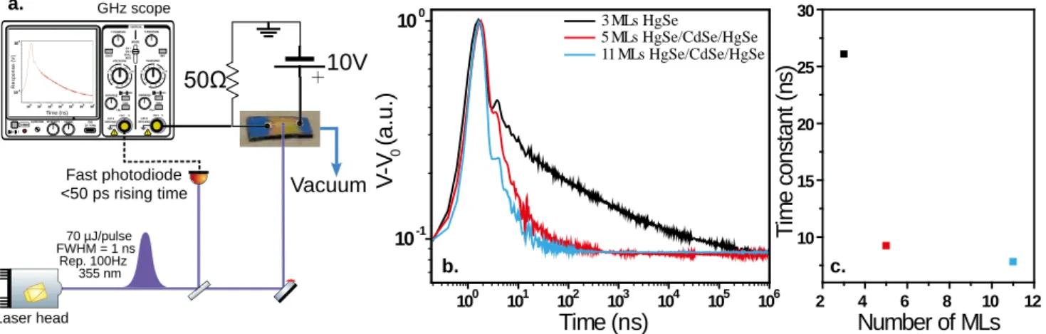
Figure 4 (a.) Scheme of the transient photocurrent setup. (b.) Normalized transient photocurrent signal for CdSe-HgSe heterostructures of different thicknesses. (c.) Transient photocurrent decay time as a function of the NPLs thickness.
To finish, we discuss the dynamics of carriers into these heterostructures. So far, these NPLs do not present photoluminescence (PL) and traditional time resolved PL cannot be used to probe carrier relaxation. Other methods such as transient absorption and time resolved photoemission52 can be used as alternative probe. Here, we rather choose to
study the photoconductive properties of the material through time resolved transient photocurrent measurements53. After
a fast ns UV laser excitation, we follow the rise and decay of the photocurrent on a GHz oscilloscope of a film of NPLs, see Figure 4a for a scheme of the setup. The rise of the current is typically limited by the light pulse. This rise is first followed by a fast decay during the first ns whatever the sample. Then a dependent thickness decay appears at longer time scales, see Figure 4b. We observe that the thicker the NPLs are, the faster they respond (see Figure 4c). HgSe NPLs present a long tail of photocurrent, which expands up to 1 ms after pulse (black curve on Figure 4b). Recently it was proposed, in narrow band gap HgTe NCs that such tail is the signature of multitrapping process.53 After excitation, the
carriers can either recombine or get trap. Once trapped, the dynamics of the system is driven by the trapped carriers release time. And the deeper the traps are, the longer the release lasts. The faster dynamics observed in the heterostructures suggests a limited role of traps. This is consistent with our previous observation that transport is driven by the CdSe core and is thus less sensitive to the external traps thanks to the presence of the HgSe shell.
CONCLUSION
We have grown a 2D heterostructure combining both a wide band gap and a narrow band gap material. These HgSe/CdSe/HgSe heterostructures are obtained thanks to a cation exchange happening on exactly two cationic layers on the equivalent top and bottom facets of CdSe NPLs. The interface between the two materials is topotaxial. By carefully choosing the two materials and hence the effective mass of their carriers, it is possible to make the optical feature only determined by the narrow band gap material, in spite of the quasi-type II band alignment. Even more interestingly is the fact that transport properties are driven by the wide band gap core material. We observe that in presence of a CdSe barrier, the heterostructures present an electrical gap which can be wider (by 300 meV) than its
2 4 6 8 10 12 10 15 20 25 30 T im e co n st a n t (n s) Number of MLs 100 101 102 103 104 105 106 10-1 100 3 MLs HgSe 5 MLs HgSe/CdSe/HgSe 11 MLs HgSe/CdSe/HgSe V -V0 (a.u.) Time (ns) Vacuum Laser head 50Ω 70 µJ/pulse FWHM = 1 ns Rep. 100Hz 355 nm Fast photodiode <50 ps rising time GHz scope 10V 10010110210310410510 10-1 100 R e s p o n s e ( V ) Time (ns) 6 b. c. a.
optical gap. This strategy is extremely useful for future development of IR active layer based on NCs for infrared photodetection where dark current is a key limitation.
Supporting informations
Supporting information include details about absorption kinetics from CdSe to HgSe 3 ML NPLs; TEM images of NPLs before and after cation exchange; absorption spectra from 6 to 11 ML NPLs; X-ray diffraction patterns of NPLs; energy dispersive X-ray spectroscopy (EDX); Rutherford Backscattering Spectrometry, numerical simulation; ligand exchange and fabrication of field effect transistors; time resolved measurements
ACKNOWLEDEGMENTS
This work has been supported by the Region Ile-de-France in the framework of DIM Nano-K (grant dopQD). This work was supported by French state funds managed by the ANR within the Investissements d'Avenir programme under reference ANR-11-IDEX-0004-02, and more specifically within the framework of the Cluster of Excellence MATISSE and also by the grant Nanodose and H2DH. EL thanks the support ERC starting grant blackQD (grant number 756225). GP thanks the Equipex TEMPOS referenced 10-EPQX-0050. We acknowledge the use of clean-room facilities from the “Centrale de Proximité Paris-Centre”.
REFERENCES
(1) Lhuillier, E.; Scarafagio, M.; Hease, P.; Nadal, B.; Aubin, H.; Xu, X. Z.; Lequeux, N.; Patriarche, G.; Ithurria, S.; Dubertret, B. Infrared Photodetection Based on Colloidal Quantum-Dot Films with High Mobility and Optical Absorption up to THz. Nano Lett. 2016, 16 (2), 1282–1286.
(2) Brokmann, X.; Messin, G.; Desbiolles, P.; Giacobino, E.; Dahan, M.; Hermier, J. P. Colloidal CdSe/ZnS Quantum Dots as Single-Photon Sources. New J. Phys. 2004, 6, 1–8.
(3) Geiregat, P.; Houtepen, A. J.; Sagar, L. K.; Infante, I.; Zapata, F.; Grigel, V.; Allan, G.; Delerue, C.; Van Thourhout, D.; Hens, Z. Continuous-Wave Infrared Optical Gain and Amplified Spontaneous Emission at Ultralow Threshold by Colloidal HgTe Quantum Dots. Nat. Mater. 2017, 17 (October 2017), 35–42.
(4) Fan, F.; Voznyy, O.; Sabatini, R. P.; Bicanic, K. T.; Adachi, M. M.; McBride, J. R.; Reid, K. R.; Park, Y. S.; Li, X.; Jain, A.; Quintero-Bermudez, R.; Saravanapavanantham, M.; Liu, M.; Korkusinski, M.; Hawrylak, P.; Klimov, V. I.; Rosenthal, S. J.; Hoogland, S.; Sargent, E. H. Continuous-Wave Lasing in Colloidal Quantum Dot Solids Enabled by Facet-Selective Epitaxy. Nature 2017, 544 (7648), 75–79.
(5) Lim, J.; Park, Y.-S.; Klimov, V. I. Optical Gain in Colloidal Quantum Dots Achieved with Direct-Current Electrical Pumping. Nat. Mater. 2017, 17 (November 2017), 42–48.
(6) Liu, H. C.; Schneider, H. Quantum Well Infrared Photodetectors; Springer, 2006.
(7) Levine, B. F. Quantum‐well Infrared Photodetectors. J. Appl. Phys. 1993, 74 (8), R1–R81.
(8) Gendron, L.; Carras, M.; Huynh, A.; Ortiz, V.; Koeniguer, C.; Berger, V. Quantum Cascade Photodetector.
Appl. Phys. Lett. 2004, 85 (14), 2824–2826.
(9) Hofstetter, D.; Beck, M.; Faist, J. Quantum-Cascade-Laser Structures as Photodetectors. Appl. Phys. Lett. 2002, 81 (15), 2683–2685.
(10) Faist, J.; Capasso, F.; Sivco, D. L.; Sirtori, C.; Hutchinson, A. L.; Cho, A. Y. Quantum Cascade Laser. Science
(80-. ). 1994, 264 (5158), 553–556.
Roughness Transport in Terahertz Quantum Cascade Detectors. Appl. Phys. Lett. 2010, 96 (6), 108–111. (12) Hines, M. A.; Guyot-Sionnest, P. Synthesis and Characterization of Strongly Luminescing ZnS-Capped CdSe
Nanocrystals. J. Phys. Chem. 1996, 100 (2), 468–471.
(13) Soni, U.; Pal, A.; Singh, S.; Mittal, M.; Yadav, S.; Elangovan, R.; Sapra, S. Simultaneous Type-I/Type-II Emission from CdSe/CdS/ZnSe Nano-Heterostructures. ACS Nano 2014, 8 (1), 113–123.
(14) Carbone, L.; Nobile, C.; De Giorgi, M.; Della Sala, F.; Morello, G.; Pompa, P.; Hytch, M.; Snoeck, E.; Fiore, A.; Franchini, I. R.; Nadasan, M.; Silvestre, A. F.; Chiodo, L.; Kudera, S.; Cingolani, R.; Krahne, R.; Manna, L. Synthesis and Micrometer-Scale Assembly of Colloidal CdSe/CdS Nanorods Prepared by a Seeded Growth Approach. Nano Lett. 2007, 7 (10), 2942–2950.
(15) Cassette, E.; Mahler, B.; Guigner, J. M.; Patriarche, G.; Dubertret, B.; Pons, T. Colloidal CdSe/CdS Dot-in-Plate Nanocrystals with 2D-Polarized Emission. ACS Nano 2012, 6 (8), 6741–6750.
(16) Piryatinski, A.; Ivanov, S. A.; Tretiak, S.; Klimov, V. I. Effect of Quantum and Dielectric Confinement on the Exciton-Exciton Interaction Energy in Type II Core/shell Semiconductor Nanocrystals. Nano Lett. 2007, 7 (1), 108–115.
(17) Chuang, C. H.; Lo, S. S.; Scholes, G. D.; Burda, C. Charge Separation and Recombination in CdTe/CdSe Core/shell Nanocrystals as a Function of Shell Coverage: Probing the Onset of the Quasi Type-II Regime. J.
Phys. Chem. Lett. 2010, 1 (17), 2530–2535.
(18) Cragg, G. E.; Efros, A. L. Suppression of Auger Processes in Confined Structures. Nano Lett. 2010, 10 (1), 313–317.
(19) Lhuillier, E.; Guyot-Sionnest, P. Recent Progresses in Mid Infrared Nanocrystal Optoelectronics. IEEE J. Sel.
Top. Quantum Electron. 2017, 23 (5), 1–8.
(20) Eychmüller, A.; Mews, A.; Weller, H. A Quantum Dot Quantum Well: CdS/HgS/CdS. Chem. Phys. Lett. 1993,
208 (1–2), 59–62.
(21) Kershaw, S. V; Burt, M.; Harrison, M.; Rogach, A.; Weller, H.; Eychmüller, A. Colloidal CdTe/HgTe Quantum Dots with High Photoluminescence Quantum Efficiency at Room Temperature. Appl. Phys. Lett.
Appl. Phys. Lett. 1999, 75 (101), 1694–1696.
(22) Schooss, D.; Mews, A.; Eychmüller, A.; Weller, H. Quantum-Dot Quantum Well CdS/HgS/CdS: Theory and Experiment. Phys. Rev. B 1994, 49 (24), 17072–17078.
(23) Lhuillier, E.; Pedetti, S.; Ithurria, S.; Nadal, B.; Heuclin, H.; Dubertret, B. Two-Dimensional Colloidal Metal Chalcogenides Semiconductors: Synthesis, Spectroscopy, and Applications. Acc. Chem. Res. 2015, 48 (1), 22– 30.
(24) Nasilowski, M.; Mahler, B.; Lhuillier, E.; Ithurria, S.; Dubertret, B. Two-Dimensional Colloidal Nanocrystals.
Chem. Rev. 2016, 116 (18), 10934–10982.
(25) Izquierdo, E.; Robin, A.; Keuleyan, S.; Lequeux, N.; Lhuillier, E.; Ithurria, S. Strongly Confined HgTe 2D Nanoplatelets as Narrow Near-Infrared Emitters. J. Am. Chem. Soc. 2016, 138 (33), 10496–10501.
(26) Lhuillier, E.; Keuleyan, S.; Guyot-Sionnest, P. Corrigendum: Optical Properties of HgTe Colloidal Quantum Dots (2012 Nanotechnology 23 175705). Nanotechnology 2014, 25 (189501), 1–6.
(27) Riedinger, A.; Ott, F. D.; Mule, A.; Mazzotti, S.; Knüsel, P. N.; Kress, S. J. P.; Prins, F.; Erwin, S. C.; Norris, D. J. An Intrinsic Growth Instability in Isotropic Materials Leads to Quasi-Two-Dimensional Nanoplatelets.
Nat. Mater. 2017, 16 (7), 743–748.
(28) Chen, Y.; Chen, D.; Li, Z.; Peng, X. Symmetry-Breaking for Formation of Rectangular CdSe Two-Dimensional Nanocrystals in Zinc-Blende Structure. J. Am. Chem. Soc. 2017, 139 (29), 10009–10019.
Zinc and Lead Chalcogenide Core and Core/shell Nanoplatelets Using Sequential Cation Exchange Reactions.
Chem. Mater. 2014, 26 (9), 3002–3008.
(30) Ithurria, S.; Talapin, D. V. Colloidal Atomic Layer Deposition (c-ALD) Using Self-Limiting Reactions at Nanocrystal Surface Coupled to Phase Transfer between Polar and Nonpolar Media. J. Am. Chem. Soc. 2012,
134 (45), 18585–18590.
(31) Prudnikau, A.; Chuvilin, A.; Artemyev, M. CdSe-CdS Nanoheteroplatelets with Efficient Photoexcitation of Central CdSe Region through Epitaxially Grown CdS Wings. J. Am. Chem. Soc. 2013, 135 (39), 14476–14479. (32) Choi, D.; Yoon, B.; Kim, D.-K.; Baik, H.; Choi, J.-H.; Jeong, K. S. Major Electronic Transition Shift from
Bandgap to Localized Surface Plasmon Resonance in Cd X Hg 1– X Se Alloy Nanocrystals. Chem. Mater. 2017, 29, 8548–8554.
(33) Shen, G.; Guyot-Sionnest, P. HgS and HgS/CdS Colloidal Quantum Dots with Infrared Intraband Transitions and Emergence of a Surface Plasmon. J. Phys. Chem. C 2016, 120 (21), 11744–11753.
(34) Robin, A.; Livache, C.; Ithurria, S.; Lacaze, E.; Dubertret, B.; Lhuillier, E. Surface Control of Doping in Self-Doped Nanocrystals. ACS Appl. Mater. Interfaces 2016, 8 (40), 27122–27128.
(35) Sagar, L. K.; Walravens, W.; Maes, J.; Geiregat, P.; Hens, Z. HgSe/CdE (E = S, Se) Core/Shell Nanocrystals by Colloidal Atomic Layer Deposition. J. Phys. Chem. C 2017, 121 (25), 13816–13822.
(36) Chu, A.; Livache, C.; Ithurria, S.; Lhuillier, E. Electronic Structure Robustness and Design Rules for 2D Colloidal Heterostructures. J. Appl. Phys. 2018, 123 (35701), 1–6.
(37) Ithurria, S.; Tessier, M. D.; Mahler, B.; Lobo, R. P. S. M.; Dubertret, B.; Efros, A. L. Colloidal Nanoplatelets with Two-Dimensional Electronic Structure. Nat. Mater. 2011, 10 (12), 936–941.
(38) Lhuillier, E.; Pedetti, S.; Ithurria, S.; Heuclin, H.; Nadal, B.; Robin, A.; Patriarche, G.; Lequeux, N.; Dubertret, B. Electrolyte-Gated Field Effect Transistor to Probe the Surface Defects and Morphology in Films of Thick CdSe Colloidal Nanoplatelets. ACS Nano 2014, 8 (4), 3813–3820.
(39) Sagar, L. K.; Walravens, W.; Zhao, Q.; Vantomme, A.; Geiregat, P.; Hens, Z. PbS/CdS Core/shell Quantum Dots by Additive, Layer-by-Layer Shell Growth. Chem. Mater. 2016, 28 (19), 6953–6959.
(40) Smith, A. M.; Nie, S. Bright and Compact Alloyed Quantum Dots with Broadly Tunable near-Infrared Absorption and Fluorescence Spectra through Mercury Cation Exchange. J. 2011, pp 24–26.
(41) Smith, A. M.; Lane, L. A.; Nie, S. Mapping the Spatial Distribution of Charge Carriers in Quantum-Confined Heterostructures. Nat. Commun. 2014, 5 (4506), 1–12.
(42) Kershaw, S. V.; Abdelazim, N. M.; Zhao, Y.; Susha, A. S.; Zhovtiuk, O.; Teoh, W. Y.; Rogach, A. L. Investigation of the Exchange Kinetics and Surface Recovery of CdxHg1-xTe Quantum Dots during Cation Exchange Using a Microfluidic Flow Reactor. Chem. Mater. 2017, 29 (7), 2756–2768.
(43) Antanovich, a.; Achtstein, a. W.; Matsukovich, a.; Prudnikau, a.; Bhaskar, P.; Gurin, V.; Molinari, M.; Artemyev, M. A Strain-Induced Exciton Transition Energy Shift in CdSe Nanoplatelets: The Impact of an Organic Ligand Shell. Nanoscale 2017, 9 (45), 18042–18053.
(44) Strauch, D. CdSe: Bulk Modulus, Compressibility.; Rössler, Ulrich, E., Ed.; Springer, Berlin, Heidelberg, 2012; pp 136–140.
(45) Kumazaki, K. Elastic Constants and Inoicity of Semimetallic HgSe. Phys. Status Solidi 1975, 29, 55–58. (46) Eich, D.; Hübner, D.; Ortner, K.; Kilian, L.; Becker, R.; Landwehr, G.; Fink, R.; Umbach, E. Photoemission
Investigation of MBE-Grown HgSe/CdSe Heterostructures. Appl. Surf. Sci. 2000, 166 (1–4), 12–16.
(47) Benchamekh, R.; Gippius, N. A.; Even, J.; Nestoklon, M. O.; Jancu, J. M.; Ithurria, S.; Dubertret, B.; Efros, A. L.; Voisin, P. Tight-Binding Calculations of Image-Charge Effects in Colloidal Nanoscale Platelets of CdSe.
(48) Rajadell, F.; Climente, J. I.; Planelles, J. Excitons in Core-Only, Core-Shell and Core-Crown CdSe Nanoplatelets: Interplay between in-Plane Electron-Hole Correlation, Spatial Confinement, and Dielectric Confinement. Phys. Rev. B 2017, 96 (3), 1–10.
(49) Achtstein, A. W.; Schliwa, A.; Prudnikau, A.; Hardzei, M.; Artemyev, M. V.; Thomsen, C.; Woggon, U. Electronic Structure and Exciton-Phonon Interaction in Two-Dimensional Colloidal Cdse Nanosheets. Nano
Lett. 2012, 12 (6), 3151–3157.
(50) Nag, A.; Kovalenko, M. V.; Lee, J. S.; Liu, W.; Spokoyny, B.; Talapin, D. V. Metal-Free Inorganic Ligands for Colloidal Nanocrystals: S2-, HS-, Se2-, HSe-, Te2-, HTe-, TeS32-, OH-, and NH2-as Surface Ligands. J.
Am. Chem. Soc. 2011, 133 (27), 10612–10620.
(51) Lhuillier, E.; Ithurria, S.; Descamps-Mandine, A.; Douillard, T.; Castaing, R.; Xu, X. Z.; Taberna, P. L.; Simon, P.; Aubin, H.; Dubertret, B. Investigating the N- and P-Type Electrolytic Charging of Colloidal Nanoplatelets. J. Phys. Chem. C 2015, 119 (38), 21795–21799.
(52) Livache, C.; Izquierdo, E.; Martinez, B.; Dufour, M.; Pierucci, D.; Keuleyan, S.; Cruguel, H.; Becerra, L.; Fave, J. L.; Aubin, H.; Ouerghi, A.; Lacaze, E.; Silly, M. G.; Dubertret, B.; Ithurria, S.; Lhuillier, E. Charge Dynamics and Optolectronic Properties in HgTe Colloidal Quantum Wells. Nano Lett. 2017, 17 (7), 4067– 4074.
(53) Martinez, B.; Livache, C.; Goubet, N.; Jagtap, A.; Cruguel, H.; Ouerghi, A.; Lacaze, E.; Silly, M. G.; Lhuillier, E. Probing Charge Carrier Dynamics to Unveil the Role of Surface Ligands in HgTe Narrow Band Gap Nanocrystals. J. Phys. Chem. C 2018, 122 (1), 859–865.