Design rules for net absorption enhancement in
pseudo-disordered photonic crystal for thin film
solar cells
He Ding,1,2 Loïc Lalouat,1,2 Bastian Gonzalez-Acevedo,1,2 Régis Orobtchouk,1,3 Christian Seassal,1,2 and Emmanuel Drouard1,2,*
1Université de Lyon, Institut des Nanotechnologies de Lyon (INL) UMR 5270 CNRS-INSA-ECL-UCBL, France 2Ecole Centrale de Lyon, 36 avenue Guy de Collongue, 69134, Ecully Cedex, France
3INSA de Lyon, Bat. Blaise Pascal, 7 avenue Jean Capelle, 69621, Villeurbanne, France *emmanuel.drouard@ec-lyon.fr
Abstract: The role of pseudo-disordered photonic crystals on the
absorption efficiency of simplified thin film crystalline silicon solar cells is presented and discussed. The expected short circuit current can thus be further increased compared to a fully optimized square lattice of holes, thanks to carefully controlled positions of the nanoholes in the considered realistic simplified solar cell stack. In addition, the pseudo-disordered structures are less sensitive to the angle of incidence, especially in the long wavelength range.
©2016 Optical Society of America
OCIS codes: (230.5298) Photonic crystals; (040.5350) Photovoltaic. References and links
1. X. Meng, V. Depauw, G. Gomard, O. El Daif, C. Trompoukis, E. Drouard, C. Jamois, A. Fave, F. Dross, I. Gordon, and C. Seassal, “Design, fabrication and optical characterization of photonic crystal assisted thin film monocrystalline-silicon solar cells,” Opt. Express 20(S4), A465–A475 (2012).
2. K. R. Catchpole and A. Polman, “Plasmonic solar cells,” Opt. Express 16(26), 21793–21800 (2008). 3. H. A. Atwater and A. Polman, “Plasmonics for improved photovoltaic devices,” Nat. Mater. 9(3), 205–213
(2010).
4. E. Garnett and P. Yang, “Light trapping in silicon nanowire solar cells,” Nano Lett. 10(3), 1082–1087 (2010). 5. R. Dewan, V. Jovanov, S. Hamraz, and D. Knipp, “Analyzing periodic and random textured silicon thin film
solar cells by Rigorous Coupled Wave Analysis,” Sci. Rep. 4, 6029 (2014).
6. M. Burresi, F. Pratesi, F. Riboli, and D. S. Wiersma, “Complex photonic structures for light harvesting,” Adv. Opt. Mater. 3(6), 722–743 (2015).
7. M. S. Branham, W. C. Hsu, S. Yerci, J. Loomis, S. V. Boriskina, B. R. Hoard, S. E. Han, and G. Chen, “15.7% efficient 10-μm-thick crystalline silicon solar cells using periodic nanostructures,” Adv. Mater. 27(13), 2182– 2188 (2015).
8. L. Zeng, P. Bermel, Y. Yi, B. Alamariu, K. Broderick, J. Liu, C. Hong, X. Duan, J. Joannopoulos, and L. Kimerling, “Demonstration of enhanced absorption in thin film Si solar cells with textured photonic crystal back reflector,” Appl. Phys. Lett. 93(22), 221105 (2008).
9. J. G. Mutitu, S. Shi, C. Chen, T. Creazzo, A. Barnett, C. Honsberg, and D. W. Prather, “Thin film solar cell design based on photonic crystal and diffractive grating structures,” Opt. Express 16(19), 15238–15248 (2008). 10. X. Meng, E. Drouard, G. Gomard, R. Peretti, A. Fave, and C. Seassal, “Combined front and back diffraction
gratings for broad band light trapping in thin film solar cell,” Opt. Express 20(S5), A560–A571 (2012). 11. C. S. Schuster, P. Kowalczewski, E. R. Martins, M. Patrini, M. G. Scullion, M. Liscidini, L. Lewis, C. Reardon,
L. C. Andreani, and T. F. Krauss, “Dual gratings for enhanced light trapping in thin-film solar cells by a layer-transfer technique,” Opt. Express 21(S3), A433–A439 (2013).
12. K. Vynck, M. Burresi, F. Riboli, and D. S. Wiersma, “Photon management in two-dimensional disordered media,” Nat. Mater. 11(12), 1017–1022 (2012).
13. F. Pratesi, M. Burresi, F. Riboli, K. Vynck, and D. S. Wiersma, “Disordered photonic structures for light harvesting in solar cells,” Opt. Express 21(S3), A460–A468 (2013).
14. M. Burresi, F. Pratesi, K. Vynck, M. Prasciolu, M. Tormen, and D. S. Wiersma, “Two-dimensional disorder for broadband, omnidirectional and polarization-insensitive absorption,” Opt. Express 21(S2), A268–A275 (2013). 15. U. W. Paetzold, M. Smeets, M. Meier, K. Bittkau, T. Merdzhanova, V. Smirnov, D. Michaelis, C. Waechter, R. Carius, and U. Rau, “Disorder improves nanophotonic light trapping in thin-film solar cells,” Appl. Phys. Lett. 104(13), 131102 (2014).
16. R. A. Pala, J. S. Liu, E. S. Barnard, D. Askarov, E. C. Garnett, S. Fan, and M. L. Brongersma, “Optimization of non-periodic plasmonic light-trapping layers for thin-film solar cells,” Nat. Commun. 4, 2095 (2013).
17. Q. G. Du, C. H. Kam, H. V. Demir, H. Y. Yu, and X. W. Sun, “Broadband absorption enhancement in randomly positioned silicon nanowire arrays for solar cell applications,” Opt. Lett. 36(10), 1884–1886 (2011).
18. A. Oskooi, P. A. Favuzzi, Y. Tanaka, H. Shigeta, Y. Kawakami, and S. Noda, “Partially disordered photonic-crystal thin films for enhanced and robust photovoltaics,” Appl. Phys. Lett. 100(18), 181110 (2012). 19. C. Lin, L. J. Martínez, and M. L. Povinelli, “Experimental broadband absorption enhancement in silicon
nanohole structures with optimized complex unit cells,” Opt. Express 21(S5), A872–A882 (2013). 20. E. R. Martins, J. Li, Y. Liu, V. Depauw, Z. Chen, J. Zhou, and T. F. Krauss, “Deterministic quasi-random
nanostructures for photon control,” Nat. Commun. 4, 2665 (2013).
21. R. Peretti, G. Gomard, L. Lalouat, C. Seassal, and E. Drouard, “Absorption control in pseudodisordered photonic-crystal thin films,” Phys. Rev. A 88(5), 053835 (2013).
22. J. Liu, L. Lalouat, E. Drouard, and R. Orobtchouk, “Binary coded patterns for photon control using necklace problem concept,” Opt. Express 24(2), 1133–1142 (2016).
23. A. Oskooi, Y. Tanaka, and S. Noda, “Tandem photonic-crystal thin films surpassing Lambertian light-trapping limit over broad bandwidth and angular range,” Appl. Phys. Lett. 104(9), 091121 (2014).
24. A. Oskooi, M. De Zoysa, K. Ishizaki, and S. Noda, “Experimental Demonstration of Quasi-resonant Absorption in Silicon Thin Films for Enhanced Solar Light Trapping,” ACS Photonics 1(4), 304–309 (2014).
25. X. Fang, M. Lou, H. Bao, and C. Y. Zhao, “Thin films with disordered nanohole patterns for solar radiation absorbers,” J. Quant. Spectrosc. Radiat. Transf. 158, 145–153 (2015).
26. H. Ren, Q. Du, F. Ren, and C. Png, “Photonic quasicrystal nanopatterned silicon thin film for photovoltaic applications,” J. Opt. 17(3), 035901 (2015).
27. P. A. Postigo and J. M. Llorens, “Optical absorption enhancement by photonic quasicrystals in thin films for photovoltaic applications,” in 2013 15th International Conference on Transparent Optical Networks (ICTON) (2013), pp. 1–4.
28. J. Xavier, J. Probst, F. Back, P. Wyss, D. Eisenhauer, B. Löchel, E. Rudigier-Voigt, and C. Becker, “Quasicrystalline-structured light harvesting nanophotonic silicon films on nanoimprinted glass for ultra-thin photovoltaics,” Opt. Mater. Express 4(11), 2290–2299 (2014).
29. M. C. van Lare and A. Polman, “Optimized scattering power spectral density of photovoltaic light-trapping patterns,” ACS Photonics 2(7), 822–831 (2015).
30. A. Bozzola, M. Liscidini, and L. C. Andreani, “Photonic light-trapping versus Lambertian limits in thin film silicon solar cells with 1D and 2D periodic patterns,” Opt. Express 20(S2), A224–A244 (2012).
31. V. Depauw, X. Meng, O. El Daif, G. Gomard, L. Lalouat, E. Drouard, C. Trompoukis, A. Fave, C. Seassal, and I. Gordon, “Micrometer-thin crystalline-silicon solar cells integrating numerically optimized 2-D photonic crystals,” IEEE J. Photovoltaics 4(1), 215–223 (2014).
32. M. Moharam and T. Gaylord, “Rigorous coupled-wave analysis of planar-grating diffraction,” J. Opt. Soc. Am. 71(7), 811–818 (1981).
33. C. Herzinger, B. Johs, W. McGahan, J. Woollam, and W. Paulson, “Ellipsometric determination of optical constants for silicon and thermally grown silicon dioxide via a multi-sample, multi-wavelength, multi-angle investigation,” J. Appl. Phys. 83(6), 3323–3336 (1998).
34. E. D. Palik, Handbook of Optical Constants of Solids, Vol. 3 (Academic Press, 1998). 35. Source of data ASTM/NREL, http://rredc.nrel.gov/solar/spectra/am1.5/.
36. T. Tiedje, E. Yablonovitch, G. D. Cody, and B. G. Brooks, “Limiting efficiency of silicon solar cells,” IEEE Trans. Electron Dev. 31(5), 711–716 (1984).
37. G. Gomard, R. Peretti, E. Drouard, X. Meng, and C. Seassal, “Photonic crystals and optical mode engineering for thin film photovoltaics,” Opt. Express 21(S3), A515–A527 (2013).
38. A. Bozzola, M. Liscidini, and L. C. Andreani, “Broadband light trapping with disordered photonic structures in thin-film silicon solar cells,” Prog. Photovolt. Res. Appl. 22, 1237–1245 (2014).
39. Z. Yu, A. Raman, and S. Fan, “Fundamental limit of light trapping in grating structures,” Opt. Express 18(S3 Suppl 3), A366–A380 (2010).
40. C. Trompoukis, O. El Daif, V. Depauw, I. Gordon, and J. Poortmans, “Photonic assisted light trapping integrated in ultrathin crystalline silicon solar cells by nanoimprint lithography,” Appl. Phys. Lett. 101(10), 103901 (2012). 1. Introduction
A wide range of photon management schemes, based on photonic crystals (PC) [1], plasmonics [2, 3], nanowires [4] or random textured surface [5], have been proposed to enable efficient light trapping in thin film (<10 µm thick) solar cells. Among these possibilities, using a PC structure [6, 7] is a quite flexible and promising strategy relying on diffraction to couple the light into the absorbing layer, thereby to increase the absorption. Moreover, an increase of the open-circuit voltage can be expected due to improved carrier collection, provided the surfaces are passivated.
In the recent years, many investigations and optimizations have taken advantage of nanopatterns, such as gratings or PC structures inserted on the front [1], rear [8, 9] or both sides [10, 11] of the thin film solar cell. Although solar cells including optimized and ordered PC structures exhibit a higher absorption compared to an unpatterned flat structure, the absorption in the long wavelength range (i.e. where the absorption coefficient of the material is low) still needs to be improved. The reason is that only few guided mode resonances can be exploited to achieve light trapping in simply periodic structures.
The mechanism of light coupling and trapping into thin film solar cells can be further improved by using additional resonant modes in the long wavelength range. To achieve this, introducing a certain degree of disorder in a periodic structure has been considered during the past years. However, in most of these investigations, the performance of disordered structures [12–17], partly disordered structures [18–26] or quasicrystal structures [27, 28] are compared to non-optimized ordered structure [12, 13, 15, 19, 24]. Meanwhile, only very low thicknesses (≤ 1 µm) have been considered in most studies, leading to a low expected short circuit current for the final devices. To reach high levels of short circuit currents, using a high quality material like crystalline silicon (c-Si) with a thickness in excess of 1 µm should therefore considered. Furthermore, most of these theoretical investigations consider the sole absorbing layer [12, 19, 21, 25, 26], i.e. without a back metal layer, or nanopatterns which fabrication appears highly challenging [20, 29]. In Ref [21], we have analyzed in detail a few pseudo-disordered structures made of supercells of randomly located holes, periodically repeated in a square lattice, in the case of a simple 195 nm thick hydrogenated amorphous silicon layer on glass. It has been shown that resulting broader resonances together with a higher spectral density of modes can further enhance the absorption.
In this manuscript we first consider as references fully optimized square lattice PC in a simplified realistic thin solar cell stack, as it includes a metallic back reflector and a top transparent electrode. The considered thicknesses of the c-Si layer are in the 1-8 µm range. If low thicknesses could easily exhibit stronger current improvements, 8 µm layer exhibits high current densities, typically around 30 mA/cm2 [30]. We then investigate numerically the
absorption performances of such structures, both in the real and Fourier space, with a view to determine design guidelines to enable a net increase of the absorption.
Section 2 is dedicated to the description of the considered solar cells stack and the simulation methodology. Optimized square lattice of holes for several thicknesses of c-Si are presented in section 3. In sections 4 and 5, the effect of the pseudo-disorder is investigated numerically and analyzed in real space as well as in the reciprocal space. The angular response of the patterned stack is discussed in the last section of the manuscript.
2. Thin film solar cells design and simulation methodology
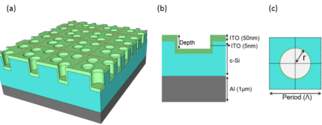
The simplified solar cell stack considered in this work is depicted in Fig. 1(a). It consists of a thin absorbing layer of c-Si bonded onto a 1 µm thick aluminum (Al) layer that acts as a back mirror and back contact. Then a 2D PC structure is patterned on top of the c-Si layer, as depicted in Figs. 1(b) and 1(c). Finally, the patterned c-Si layer is covered by a continuous indium tin oxide (ITO) layer. This layer acts as the transparent front electrode of the solar cell, as in [30]. As shown in Fig. 1(b), the thickness of the ITO layer is not the same for horizontal surfaces and sidewalls, as it is the case for fabricated solar cells [31].
In order to determine the absorption, we resort to the rigorous coupled wave analysis (RCWA) method [32]. In this in-house developed RCWA code, for each cylindrical hole, analytical Bessel functions are used to calculate the Fourier coefficients of the permittivity, rather than the Fast Fourier transform (FFT) techniques. This enables a faster computation. Moreover, In contrast to most of other methods, the computation time does not depend from the thickness of the stack, for a given spectral resolution. The number of orders used in the simulation, from −4 to + 4 in each direction for the square lattice of holes, ensures to reach accurate results. Indeed, there is only a 0.2% discrepancy in the integrated absorption with a
calculation using orders in the range [-5, 5], and this difference is concentrated in the low wavelength range, where the impact of the pseudo-disorder will appear to be negligible. Optical indices of the materials are presented in appendix [33, 34]. Unpolarized light (averaged of TE and TM) at normal incidence is used to mimic the solar illumination.
Fig. 1. (a) Schematic view of the simplified thin film solar cells stack with pseudo-disordered structure. Side-view (b) and top view (c) of the thin film solar cell.
The spectral range is restricted to 300-1100 nm, which is realistic for c-Si solar cells. The spectral resolution is carefully chosen considering the absorption peaks linewidth, which depends on the thickness of the c-Si layer. In the shorter wavelength range (i.e. 300-700 nm), the spectral resolution is set to 1 nm for all thicknesses of the solar cells. While in the longer wavelength range, i.e. 700-1100 nm, it is set to 0.5 nm for the 1/2/4 µm thick c-Si layers, and to 0.25 nm for the 8 µm thick case. The absorption is calculated thanks to the reflection at the front interface and the transmission at the c-Si/metal interface. It includes the parasitic absorption in ITO, still its impact remains limited (<1 mA/cm2) and almost constant for all the
considered configurations.
By assuming 100% efficiency of carrier collection, the current density (Jsc) is given by: 2 1 ( ) sc e dI J A d hc d λ λ λ λ λ λ =
(1)where e is the unit charge for an electron, h is the Planck's constant, c is speed of the light in the vacuum, λ is the wavelength, A(λ) is the absorption, and dI/dλ is the incident solar radiation intensity corresponding to the AM1.5G solar spectrum [35].
To establish a fair comparison between a pseudo-disordered structure and a simply periodic one, we first need to optimize the periodic square lattice of air holes structure. Moreover, for such comparisons, the thickness of the c-Si layer is kept constant. Indeed, even if the volume of the absorbing material is changing, such a patterning requires etching, so removing of the active material. So we choose a constant initial volume of this material, as usually (see e.g [1, 17–19, 29].).
3. Maximization of the absorption of the square lattice of cylindrical holes
The 2D square lattice of air holes is based on the elementary pattern shown in Figs. 1(b) and 1(c). It is fully determined by three parameters: the period (Λ), the air-surface filling fraction (ff) (ratio between the area of the air hole and the total area, given by ff = πr2/Λ2, r being the
radius of the cylindrical hole) and the etching depth (h). The square lattice leading to the highest Jsc is searched by scanning these three parameters within technologically realistic
ranges, as detailed in Table 1, and since according to previous studies [30], there is a single maximum. The results of the optimization are given in Table 1 for the different thicknesses of the c-Si layer, and for a stack including the Al and ITO layers.
Table 1. Achievable current density (Jsc, mA/cm2) with and without a square lattice of holes, for different thicknesses of the c-Si layer. The parameters (period, filling fraction and the depth of the hole, as well as the scanning range) correspond to the maximal value
for the optimized square lattice of holes structure. c-Si (µm)
Jsc (mA/cm2)
Period (nm) Filling fraction Etching depth (nm) Flat Square Lattice
1 13.82 19.96 620 [550 660] 0.38 [0.30 0.46] 165 [140 210] 2 17.96 23.71 570 [500 660] 0.42 [0.30 0.50] 180 [130 240] 4 21.91 27.46 620 [600 700] 0.42 [0.34 0.50] 200 [180 240] 8 25.42 30.69 650 [600 700] 0.44 [0.34 0.54] 210 [180 260]
Fig. 2. (a) Jsc calculated for the optimized geometrical parameters in the case of the square
lattice of holes with 2 µm thick c-Si layers, and for geometries modified to mimic technological fluctuations. Each step of the simulation sequence refers to a modification of each of the three key parameters, with the magnitude shown on the figure. (b) Absorption spectra of the unpatterned structure (dark line) and the optimized square lattice of holes (red line), for different thickness of the c-Si layer from 1 to 8 µm.
Thanks to the optimized square lattice of holes, the achievable Jsc exhibits a significant
increase, up to 44% for the 1µm thick layer. As expected, and observed in the case of other designs [30], this relative enhancement is limited to 21% for the 8 µm thick case, even if the volume of the pattern increases thanks to deeper holes. In order to investigate the robustness of the optimized design, we tuned each parameter (period, ff and etching depth) from its optimized value in in order to reproduce variations that arise in nanofabrication. The result for the stack including a 2 µm thick c-Si layer is shown in Fig. 2(a). These slight variations of the filling fraction (0.02 step) as well as of the etching depth (5 nm step) have a limited influence on the optical performance of the thin film solar cells: the maximal Jsc decrease is only of
can be more easily controlled than the other two during the fabrication process. This robustness of the Jsc with regards to the geometrical parameters enables a good compatibility
with standard technological processes. As shown in the following, the typical influence of the fluctuations (of the order of one step, as indicated on Fig. 2(a)) is far below the effect of the controlled perturbations introduced in pseudo-disordered structures.
Figure 2(b) shows the comparison of absorption spectra between the flat and the optimized square lattice of holes structure with different thicknesses of c-Si layer, from 1 to 8 µm. No sharp absorption peak appears in the wavelength range from 300 to 500 nm, where the penetration length of the photons in the c-Si is shorter than the absorbing layer thickness. For the wavelength range from 500 to 700 nm, several absorption resonances corresponding to the Fabry-Perot modes come out by the reflection at the c-Si/Al interface. In the 700-1100 nm, wavelength range, and compared to the unpatterned stack, the square lattice of holes structures exhibit densely packed and irregular absorption peaks due to Bloch mode resonances [1]. Besides, for each selected thickness, the absorption spectrum of the optimized square lattice of holes is almost always higher than the absorption of the flat thin-film stack. This type of behavior is well established in such stacks including simply periodic patterns in absorbing layers in the micrometer range, see e.g [1, 31].
4. Pseudo-disordered lattices of cylindrical holes
4.1 Pseudo-disordered supercells definition
In order to further increase the absorption of thin film solar cells, we propose to integrate pseudo-disordered nanopatterns. In a square lattice of holes PC, the structure is highly efficient only for specific wavelengths; this corresponds to the sharp peaks displayed in Fig. 2(b). To overcome these limitations, pseudo-disordered PC structures relying on carefully controlled positioned holes will be exploited.
Fig. 3. Schematic view of the perturbation (a) for a single hole and (b) for 9 holes in a 3 × 3 supercell structure. (c & d) Determination of the pseudo-disordered structure parameter thanks to replication of the 3 × 3 supercell. (c) The blue point represents the centroid of the selected red holes which is used to determine the “compactness” parameter. (d) The minimum distance between the 9 holes depicted by the red arrows determines the “clustering” parameter.
In such designs, each hole of a supercell is moved from its original position as shown in Fig. 3(a). The hole is shifted by a distance dp, with an angle of α. The value of dp is determined by a Gaussian distribution (e.g. dp∈
[
22 88−]
nm, σ =dp 20nm for the 2 µm c-Si thick case), while the angle is determined by a uniform distribution. Then this perturbation process is applied to N2 holes (e.g. 3 × 3, depicted in Fig. 3(b)) composing a N × N supercell.This supercell is then replicated in a square lattice. To avoid numerical issues and to keep a realistic design, only the cases in which holes do not merge are considered.
As the pattern designs are obtained by using a pseudorandom number generator (PRNG) process, the effect of the pseudo-disorder is evaluated by the protocol defined below. Since the dp is determined thanks to a Gaussian distribution, we simulated at least 10 different pseudo-disordered structures with the same mean dp value for three different supercell sizes (from 2 × 2 to 4 × 4), to obtain a representative set of patterns. This has been done for four different values of the mean dp, we additionally consider all the thickness mentioned previously (1, 2, 4 and 8 µm thick c-Si layer).
4.2 Metric parameters for pseudo-disordered structures
As shown later, supercells exhibit various shapes that can lead to very different situations, like clusters of holes or more evenly positioned and spaced holes. In order to analyze the effects of the introduced disorder in the real space, we need to define relevant metrics that can classify the pseudo-disordered structures. Thus, we define two parameters to describe the pseudo-disordered structure, in terms of clustering and compactness.
Among all the possible arrangement of holes within the lattice of supercells, we select that with the lowest mean distance between each of the N2 holes and their centroid. In the example
shown in Figs. 3(c) and 3(d), the group of N2 holes selected using this criterion corresponds to
the red circles, this group constitutes an alternative supercell to the initial square one. The compactness ratio is defined as this lowest mean distance divided by the corresponding one of the square lattice of holes. Then, for this set of N2 holes, we compute the average distance
between each hole and its nearest neighbor (Fig. 3(d)). This value, divided by the one of the square lattice of holes is the clustering ratio. Thus, a high clustering ratio corresponds to the presence of cluster(s) of holes in the supercell. It also means that a low compactness ratio associated to a high clustering ratio indicates that the pattern is made of a single cluster of N2
holes, whereas a high compactness ratio parameter with a high clustering ratio value corresponds to several clusters of holes. While one can anticipate that these two parameters are insightful for the investigation of pseudo-disordered structures, it should be noticed that they are not meant to fully describe them.
4.3 Best / worst pattern results
For each considered thickness, the mean Jsc, the standard deviation, the maximal / minimal
achievable Jsc for pseudo-disordered structures among all the calculated patterns are
summarized in Table 2, together with the corresponding supercell size and the compactness and clustering ratios. Indeed, since a pseudo disorder pattern is reproducible, it makes sense to consider not only statistical results, but also the extremes of a set of representative patterns.
Except for the smallest thickness, the mean value Jsc and even Jsc−σJsc are higher than the Jsc of the square lattice structure. This means that pseudo-disorder can easily enhance the
integrated absorption, even if it can be smaller than the reference in some cases, as can be seen with the worst Jsc values. Quite similarly, for all the considered thicknesses, the Jsc
associated to the best pseudo-disordered structure is always higher than the Jsc of the
optimized square lattice of holes. The best pseudo-disordered structures exhibit a relative increase of 2% in Jsc in the 2, 4 and 8 µm thick c-Si layer stacks, but only a very limited
increase can be obtained for the 1 µm thick c-Si layer stack. For this lowest thickness, the clustering and the compactness ratios are occasionally the same, but the distributions of the
holes are different, leading to different values of Jsc. Since the current will anyway remain
limited for 1 µm thick c-Si layer, we will focus on larger thicknesses in the following.
Table 2. Achievable current density (Jsc, mA/cm2) for the different thicknesses of c-Si layer: optimized value for square lattice of holes, mean value and standard, and extreme (best and worst) values obtained on pseudo-disordered structures with the corresponding
parameters of the pattern.
c-Si (µm) Square Lattice (Jsc, mA/cm2) Pseudo-disordered structures sc J (mA/cm²) Standard deviation σJsc (mA/cm²) Best/Worst Jsc, (mA/cm2) Difference relatively to the square lattice (%) Supercell size Compactness ratio Clustering ratio 1 19.96 19.89 0.11 20.02 0.30 2×2 1.12 1.03 19.48 -2.40 2×2 1.12 1.03 2 23.71 23.96 0.15 24.38 2.83 2×2 1.04 1.06 23.59 -0.51 2×2 0.89 1.24 4 27.46 27.69 0.09 27.95 1.78 3×3 0.96 1.09 27.51 0.18 2×2 0.91 1.22 8 30.69 30.93 0.14 31.28 1.92 2×2 0.98 1.03 30.56 -0.42 2×2 0.87 1.27
It is noticeable that for the 2 to 8 µm thick c-Si layers, the best pseudo-disordered structures always exhibit a higher clustering parameter (i.e. less clusters of holes indicated by the low clustering ratio) than the structures leading to the lowest Jsc. It should additionally be
noted that while the highest Jsc corresponds to a 2 × 2 supercell in the 2 and 8 µm thick layers,
it is a 3 × 3 supercell in the 4 µm case. Finally, since the best relative improvement with respect to the square lattice is obtained for the c-Si thickness of 2 µm, structures of this thickness will be more detailed in section 5. In addition, for a lower thickness, the best pseudo-disordered structures are achieved with a relatively low mean shift (dp≈11nm), especially for the 1 µm thick c-Si layer stack.
4.4 Absorption spectra analysis
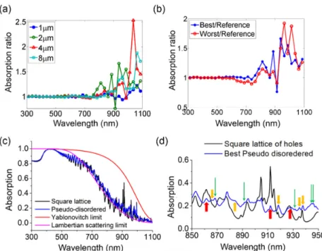
Figure 4(a) displays the ratio between the absorption in the best pseudo-disordered structures and that of the optimized square lattice of holes, in the case of the four different c-Si thicknesses considered here. On this figure, it clearly appears that the improvement mainly occurs at long wavelength range (700 – 1100 nm), where the Bloch modes can efficiently trap the incoming sun light. On the contrary, in the low wavelength range (300 – 700 nm), the pseudo-disorder does not impact the anti-reflection effect of the square lattice of hole pattern. Indeed, at the shortest wavelengths, light is absorbed within a single pass in the layer thanks to the higher extinction coefficient of silicon, especially as the thickness of the layer increases. Thus the absorption enhancement resulting from the pseudo disorder is mainly in a sharper spectral range as the thickness increases.
Fig. 4. For the 2 µm thick c-Si layer stack: (a) Ratio of the absorption associated to the best pseudo-disordered structure divided by the absorption corresponding to the optimized square lattice of holes structure. (b) Ratio of the absorption associated to the best/worst pseudo-disordered structure divided by the absorption corresponding to the optimized square lattice of holes structure. For a sake of clarity, these ratio are averaged over a 25 nm spectral range. (c) Comparison between the absorption spectra of the best pseudo-disordered structure and the optimized square lattice of holes, as well as the Yablonovitch limit and Lambertian scattering limit in the whole spectrum range; (d) for a spectral range comprised between 850 and 950 nm in order to highlight new absorption peaks (depicted by green arrows), broaden peaks (depicted by slide yellow arrows) or small magnitude peaks (depicted by red arrows).
Figure 4(b) shows the ratios between the best or worst pseudo-disordered structures and the optimized square lattice of holes, in the case of 2 µm thick c-Si layers. The main differences between these two spectra are in the 500 – 1100 nm wavelength range. The worst pseudo-disordered pattern exhibits a significantly lower (2.5% decrease) absorption than the reference optimized square lattice of holes in the 500 – 700 nm range. In the 700 – 1100 nm wavelength range, both spectra corresponding to the best and worst pseudo-disordered structures exhibit a higher absorption than the reference. The obtained enhancement for the best pseudo-disordered structure reaches a value of 10.9%, while this value is divided by a factor 2 for the worst pseudo-disordered structure. Moreover, though the absorption ratio corresponding to the worst structure is higher than the one corresponding to the best one around 1000 nm, there is less AM1.5G solar photon flux in that range, resulting in a lower enhancement.
The corresponding detailed absorption spectra are given in Fig. 4(c), still for the 2 µm thick layer stack, and compared to the Lambertian scattering limit [30] and the Yablonovitch limit [36] both under the hypothesis of a perfect mirror at the bottom interface. Even if the antireflection effect at the top of the stack is not fully optimized, the absorption of the patterned stacks is higher than the Lambertian scattering limit at large wavelengths. This shows a light trapping effect, even if it remains far below the Yablonovitch limit, also due to the fact that interferences are not taken into account in this limit. Furthermore, compared to the optimal square lattice of holes at large wavelengths (Fig. 4(d)), the absorption spectrum of the best pseudo-disordered pattern exhibits broadened peaks, and peaks with smaller amplitude. It also displays additional peaks corresponding to higher diffraction orders due to
the larger periodicity; the corresponding modes contribute to the absorption enhancement [21]. The broad and low amplitude peaks can also lead to a higher integrated absorption than sharp, high amplitude peaks [18, 24, 37].
5. Analysis of the pseudo-disordered structure
It has been shown that depending on the considered pseudo-disordered structure, the integrated absorption, and thus the Jsc, can either be increased or decreased compared to a
fully optimized square lattice of holes. So in this section, we will investigate the link between the real/reciprocal space distribution of holes inside the N × N supercell and the absorption efficiency of the simplified solar cell stacks.
5.1 Real space analysis
In order to sort the distribution of holes in the real space, we will refer to the metric parameters presented in section 4.1. For the 2 µm thick c-Si layer stack, all the results from simulation are plotted in Fig. 5(a). If few holes are too close to each other, leading to a high clustering ratio, as in the holes distributions shown in Figs. 5(c) and 5(d), the resulting Jsc is
low. If additionally, the compactness ratio is high, like for the distribution of holes in Fig. 5(b), there is only one cluster of holes within each N × N supercell and then the Jsc of the
pseudo-disordered structure is even lower.
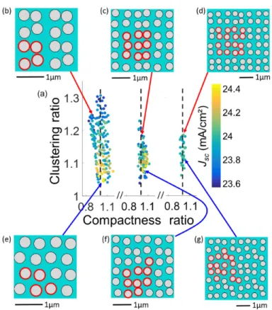
Fig. 5. Current density (Jsc, mA/cm2) map (a) as a function of clustering and compactness
parameters ratio between optimized square lattice of holes and the pseudo-disordered structure for the 2µm thick c-Si layer case. The dashed black lines represent the compactness parameter of the optimized square lattice of holes (reference value = 1) structure for 2 × 2, 3 × 3 and 4 × 4 supercell. The clustering parameter of the optimized square lattice of holes structure corresponds to the period of the lattice and is 0.57 µm. The schematic views correspond to hole distribution of the pseudo-disordered structure that exhibit lowest Jsc for 2 × 2, 3 × 3 and 4
× 4 supercells (b, c, d) highest Jsc for the same cases (e, f, g). The red circles highlight the
It can be seen in Fig. 5(a) that the spread in the clustering ratio is higher for the case of the 2 × 2 supercell. Indeed, there is more chance to get clustering of holes for smaller supercells for a given mean shift (dp). It is noticeable that the highest values of Jsc are obtained for
pseudo-disordered structures that exhibit relatively low value of the clustering ratio, as well as a compactness ratio above 1. This can be understood as they derive from distributions without several clusters of holes.
More precisely, for the 2 × 2 supercell, the statistical analysis indicates that the structure corresponding to the highest Jsc, presented in Fig. 5(e), exhibits a “homogeneous”
distribution, with evenly distributed holes and no clustering effect. On the contrary, the pseudo-disordered structure corresponding to the lowest Jsc presented in Fig. 5(b) exhibits the
opposite situation. For the 3 × 3 and 4 × 4 supercells, the highest obtained Jsc corresponds to
lower clustering ratio (Figs. 5(f) and 5(g)), even if not the lowest one. The lowest Jsc
corresponds to patterns which exhibit a strong clustering (Figs. 5(c) and 5(d)), the clustering ratio being among the highest values of the sampling.
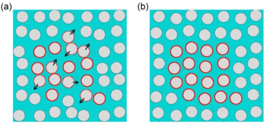
Fig. 6. Schematic view of the best 4x4 pseudo-disordered structure from the set of simulation discussed above (already shown Fig. 5d), together with the structure modified using the design rules inspired from the 2 × 2 supercell analysis. From the original distribution (a), selected holes (depicted the red dash circles) are shifted in the direction depicted by the arrow in order to break the small clusters of holes, leading to more homogeneously distributed holes (b).
It is still possible to further optimize such patterns using these conclusions as design rules, especially in the case of 4 × 4 pseudo-disordered structures. Indeed, in this case, considering that the simulations are highly time consuming, the number of situations analyzed is not sufficient to approach the optimum structure. Since the best 4 × 4 pseudo-disordered structure displayed in Fig. 5(g) still exhibits clusters of holes, this structure can be further optimized by moving the holes marked by the red dash circles in the direction shown by the arrow (Fig. 6(a)). The shifts are typically in a range of 15-90 nm. After 3 runs that all lead to a Jsc 0.2
mA/cm2 higher the J
sc of the structure of Fig. 6(a), the design leading to the highest Jsc (Fig.
6(b)) exhibits a compactness ratio increased from 1.01 to 1.03 and a low clustering ratio, 1.04 compared to 1.19 for the initial structure. As a consequence, a Jsc of 24.36 mA/cm2 is
obtained, 0.30 mA/cm2 above that corresponding to the initial 4 × 4 pseudo-disordered
structure, which is significantly higher ( + 2.7%) than the Jsc expected for the optimized
square lattice pattern. This confirms that a particular type of disorder, still far from the square lattice of hole, but with low clustering and high compactness ratios, has to be used to increase the short circuit current. It should be noted that even for this refined 4 × 4 pseudo-disordered structure, the derived Jsc remains smaller than that of the best 2 × 2 case. As all the 2 × 2
pseudo-disordered structures in 4 × 4 supercells need more permutations and combinations to achieve a fully optimal design.
While the influence of clustering and compactness ratio parameters has been discussed for the 2 µm thick c-Si layer case, similar results have been found for the 4 and 8 µm thicknesses. The negative influence of clusters of holes can be related to a result established by Bozzola et al [38] for 1D binary gratings with perturbed widths and positions. Indeed, they have found that the deviation of the pattern width should be half of the position shift, thus reducing the risk of clustering patterns. It can be also related to the only 5% averaged shift in the position compared to an optimized square lattice of holes suggested in the case of a 0.5 µm thick c-Si layer on glass in Ref [18].
In this section, we have investigated the pseudo-disordered structure in the direct space; we will now discuss on the basis of the analysis in the reciprocal space.
5.2 Spatial frequency analysis
Pseudo-disordered structures, with larger periods than the square lattices of holes, obviously exhibit richer frequencies distributions. In the following, the spatial frequencies have been integrated in the thin layer plane, over 360° in polar coordinates. As in the case of the analysis in the real space, only the stack based on the 2 µm c-Si layer will be considered.
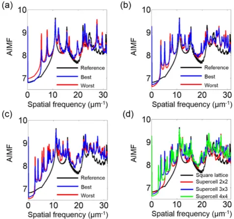
Fig. 7. Angularly integrated magnitude in logarithmic scale of Fourier component of the dielectric function of the considered nanostructure is integrated over polar coordinate (AIMF). For the 2 µm thick c-Si stack, the results for the best (res. worst) pseudo-disordered structure is plotted in blue (resp. red) line and for the optimized square lattice of holes structure in black in the case of a 2 × 2 (a), 3 × 3 (b) and 4 × 4 (c) supercell. The best pseudo-disordered structure for each supercell size and the square lattice of holes structure are also plotted together (d).
The angularly integrated magnitude (along the azimuth) of the Fourier component of the dielectric functions of few selected structures (the best and worst pseudo-disordered structures, and the optimized square lattice of holes structure), which will be referred to as the AIMF, are plotted in Figs. 7 (a)-7(c) in logarithmic scale for each supercell size. In these three figures, it appears that the AIMF of all pseudo-disordered structures are almost always higher than the ones of the optimized square lattice of holes, over the whole spatial frequency range of interest. In addition, it appears that the worst structures exhibit low spatial frequency components (<10 µm−1) with higher amplitudes than the best designs. Then focusing on the
best pseudo-disordered structures for each different supercell size (Fig. 7(d)) and compared to the optimized square lattice of holes, it is noticeable that the best Jsc is obtained in the 2 × 2
case, and corresponds to the smallest increase of the Fourier components in the low spatial frequency range (<10 µm−1).
These results can be compared to previous works on complex absorbing patterns. It is firstly supposed that at normal incidence, the diffraction efficiency of incoming light and thus the absorption of a thin layer are directly proportional to the magnitude of the Fourier component of the dielectric function. Under this assumption, Bozzola et al [38] chose to increase the diffraction efficiency in the high frequency range, which leads to a structure that makes use of numerous components of possibly high amplitude. On the other hand, Martins et al [20] directly optimized their structure in the Fourier space considering that the air light line corresponds to the limit between quasi-guided, trapped mode and photon leakage. Their optimization led to a pattern that exhibits Fourier components with low magnitude in a low frequency range, up to 2π/λ0 with λ0 corresponding to a wavelength where the absorption in
silicon becomes weak. In our case, we set the limit between the low and high frequency ranges to 2π/Λ, Λ being the period of the square lattice of holes, close to the value of λ0
chosen in [20].
Our results are then sorted according to the previous two criteria. For 2 × 2 supercell and the 2 µm thick c-Si layer stack, the current densities are displayed as a function of the AIMF over the two frequency ranges, as shown in Fig. 8. High values of Jsc are achieved for patterns
with high magnitude of the integrated dielectric function in the high frequency range, and a relatively low magnitude in the low frequency range. It then appears that both criteria suggested in the former studies mentioned above are overall satisfied.
However, since the air filling fraction is always the same as the one of the optimized square lattice of holes, the integration over the full spectral range of the square of the magnitude of the Fourier components of all structures of a given thickness is constant, according to the Parseval’s theorem. Thus, the achievable values over the two selected frequency ranges are limited. But still, such considerations could make it possible to minimize the quantity of pseudo-disordered structures to be simulated and this indicates guidelines for the optimization, which is especially valuable for large supercells.
Finally, as mentioned previously, the distribution of the Fourier components of the various structures considered have been constrained considering a fixed area filling fraction. In that sense, clusters of holes can simultaneously lead to significant diffraction at low and very high (higher than 4π/Λ) spatial frequencies, and thus may not satisfy the previous criteria. This confirms the tendency observed in the real space.
Fig. 8. Current density (Jsc, mA/cm2) map of the 2 µm thick c-Si layer stack patterned by
pseudo-disordered structures in a 2 × 2 supercell in function of the weight of low and high frequency components. The weight of low (resp. high) frequency components is determined by the AIMF in [0 2π/Λ] (resp. [2π/Λ 4π/Λ])
Fig. 9. High current density (Jsc, mA/cm2) seeking for the pseudo-disordered structure with a 5x5 supercell by referring to the criteria in terms of AIMF.
The fact that the AIMF should be low in the range [0 – 2π/Λ] of the spatial frequencies and high in the range [2π/Λ – 4π/Λ] has been used to design a 5 × 5 supercell within a 2 µm thick c-Si layer stack with a high Jsc. The two ranges are again used in Fig. 9, such as to locate
four 5 × 5 supercells that have been chosen with typical AIMF, high or low in the range [0 – 2π/Λ], and high or low in the range [2π/Λ – 4π/Λ]. Indeed, it can be checked in Fig. 9 that the
Jsc of the pattern that satisfies both criteria is higher than the one of the patterns that satisfied
only one or even none of the criteria. These criteria should thus be used as guidelines for a faster design of pseudo-disordered supercells.
All these analyses are done under normal incidence. Considering the large number of addressable optical modes, pseudo-disordered structures are also expected to be less sensitive to the angle of incidence of the impinging light. This will be investigated in the next section.
6. Angular response of the PC architectures
The absorption under oblique incidence is a critical property for photovoltaic devices without solar trackers. As depicted in Fig. 10(a) and for a nanopaterned stack, the oblique unpolarized incidence is characterized by two parameters: the incident angle (θ) and the conical angle (Φ). In order to determine Jsc under an incidence angle (θ) in a rigorous way, we calculate the
average of Jsc for all conical angles Φ (from 0° to 360° with a step of 45°).
Fig. 10. Schematic view of an oblique incident light under an incidence angle θ with a conical angle Φ (a). For the 2 µm thick c-Si layer stack, evolution of Jsc for the optimized square lattice of holes structure (red dot), for the best pseudo-disordered structures (blue triangle) and for the unpatterned case (black square) over the [300-1100] nm (b) and [700-1100] nm spectral ranges (c).
The short circuit current density predicted using this approach is plotted in Fig. 10(b) for the whole range of angles of incidence (θ), and for different structures: the unpatterned stack, the optimized square lattice of holes structure and the best pseudo-disordered structure in the 2 × 2 supercell, with 2 µm thick c-Si layers. Firstly, this shows that the Jsc value associated to
the best pseudo-disordered structure is always higher than that corresponding to the optimized square lattice of holes structure. Secondly, the optimized square lattice of holes structure exhibits an unusual increase of Jsc at small angles (around 5-10° off the vertical axis) due to
the possibility of coupling the incident light into resonances by the symmetry breaking under the oblique incidence [25, 39]. Around this angle, the difference between the optimized square lattice of holes and the best pseudo-disordered structure is the lowest; it is only 0.5% higher with the pseudo-disordered structure. For a higher angle of incidence, the difference in
Jsc increases up to 2.9%. Overall, in all cases, the Jsc decreases when the angle of incidence is
increased. This behavior is general for all types of solar cells without trackers, and is mainly due to a decrease of the incidence power density at the surface of the solar cells; this is a simple geometrical effect. As shown on the averaged spectra of Fig. 4(a), the pseudo-disorder especially impacts absorption efficiency in the long wavelength range. Focusing on the 700-1100 nm range (Fig. 10(c)), the impact of nanopatterning doubles the absorption efficiency of
a flat thin layer stack for all incidence angles. As expected, the gain between pseudo-disordered structure and square lattice of holes structure is higher for that wavelength range, with a relative increase up to 8.0%. Finally, one can notice that the Jsc fluctuations occurring
below 30° for the square lattice of holes disappear in the case of the pseudo-disordered structure, leading to a slowly decreasing Jsc for large angles of incidence.
7. Conclusion and outlook
We have studied the effect of a pseudo-disordered pattern on the absorption of technologically realistic simplified solar cell stacks including a thin absorbing c-Si layer, a front transparent electrode, and a metallic layer on the back. First, we have shown that the absorption of the pseudo-disordered structure overpasses the absorption of an optimized 2D square lattice of holes structure within a large range of c-Si layer thicknesses. Then, thanks to the metrics used to characterize the pseudo-disorder, we evidence that clustering of holes needs to be avoided to achieve a high Jsc. Studying these structures in the reciprocal space, we
have also shown that the two criteria separately suggested in the literature to optimize complex nanopatterns need to be satisfied simultaneously. The redistribution of the spatial frequencies over the whole frequency ranges is another argument against the clustering of holes. These guidelines have been used to enhance the absorption of a 5 × 5 supercell without a systematic calculation of the absorption, but rather an analysis of the structure in the reciprocal space, which is significantly faster. Pseudo-disordered structures lead to a high Jsc
not only under normal incidence, but also for a large range of angles of incidence. Lastly, according to our results, the highest Jsc has been obtained for only a 2 × 2 supercell. Indeed,
the spectral density of modes increases in N2 [21]. This could indicate that there is an optimal
density of modes to maximize the integrated absorption, so an optimal size of the supercell, as already observed in 1D patterns in [22], and like the case correlated disorder [11]. This pending question still needs further investigations.
Thanks to Nano-Imprint Lithography techniques based on replication of master stamp associated with transfer processes like plasma etching [40], the pseudo-disordered structure proposed in this communication can be realized using exactly same processes as the optimized square lattice of holes with no additional cost. Using the design rules presented in this paper together with relevant nanopatterning processes is therefore expected to lead to highly efficient and angularly stable thin film solar cells.
Appendix
The refractive indices and extinction coefficients used in the optical simulations and corresponding to c-Si [33], Al [34] and ITO [34], which are from experimental data provided by IMEC, a re displayed in Figs. 11 (a)-11(c).
Fig. 11. Refractive index n (red) and extinction coefficient k (blue) used for optical simulations, for c-Si (a), ITO (b) and Aluminum (c).
Acknowledgments
He Ding acknowledges the China Scholarship Council (CSC). This work is supported by French Research Agency (ANR) program ‘NATHISOL’ (Grant Agreement No ANR-12-PRGE-0004-01) and the European Commission Seventh Framework Programme ‘PhotoNVoltaics’ (Grant Agreement No. 309127). Valérie Depauw, from IMEC, Martin Foldyna, Pere Roca I Cabarrocas, from LPICM, and Olivier Deparis and Jérôme Muller, from UNamur, are acknowledged for fruitful discussions.