HAL Id: tel-01706954
https://tel.archives-ouvertes.fr/tel-01706954
Submitted on 12 Feb 2018HAL is a multi-disciplinary open access archive for the deposit and dissemination of sci-entific research documents, whether they are pub-lished or not. The documents may come from teaching and research institutions in France or abroad, or from public or private research centers.
L’archive ouverte pluridisciplinaire HAL, est destinée au dépôt et à la diffusion de documents scientifiques de niveau recherche, publiés ou non, émanant des établissements d’enseignement et de recherche français ou étrangers, des laboratoires publics ou privés.
heterostructures
Patrick Torresani
To cite this version:
Patrick Torresani. Hole quantum spintronics in strained germanium heterostructures. Other [cond-mat.other]. Université Grenoble Alpes, 2017. English. �NNT : 2017GREAY040�. �tel-01706954�
THÈSE
Pour obtenir le grade de
DOCTEUR DE la Communauté UNIVERSITÉ
GRENOBLE ALPES
Spécialité : Nanophysique
Arrêté ministériel : 7 Août 2006
Présentée par
TORRESANI Patrick
Thèse dirigée parDE FRANCESCHI Silvano
préparée au sein du LaTEQS, du service PHELIQS, de l’Institut NAnosciences et Cryogénie, du CEA Grenoble
et deEcole doctorale de physique
Hole
quantum
spintronics
in
strained germanium
heterostruc-tures
Thèse soutenue publiquement le14/06/2017, devant le jury composé de :
Prof. Marco Fanciulli
Università degli Studi di Milano-Bicocca, Président
Prof. Wilfred van der Wiel
University of Twente, Rapporteur
Prof. Stefano Roddaro
Scuola Normale Superiore Pisa, Rapporteur
Dr Hermann Sellier
Institut Neel, Examinateur
Dr Silvano De Franceschi
Abstract
This thesis focuses on low temperature experiments in germanium based heterostruc-ture in the scope of quantum spintronic. First, theoretical advantages of Ge for quantum spintronic are detailed, specifically the low hyperfine interaction and strong spin orbit coupling expected in Ge. In a second chapter, the theory behind quantum dots and double dots systems is explained, focusing on the aspects necessary to understand the experiments described thereafter, that is to say charging effects in quantum dots and double dots and Pauli spin blockade. The third chapter focuses on spin orbit interaction. Its origin and its effect on energy band diagrams are detailed. This chapter then focuses on consequences of the spin orbit interaction specific to two dimensional germanium het-erostructure, that is to say Rashba spin orbit interaction, D’Yakonov Perel spin relaxation mechanism and weak antilocalization.
In the fourth chapter are depicted experiments in Ge/Si core shell nanowires. In these nanowire, a quantum dot form naturally due to contact Schottky barriers and is studied. By the use of electrostatic gates, a double dot system is formed and Pauli spin blockade is revealed.
The fifth chapter reports magneto-transport measurements of a two-dimensional hole gas in a strained Ge/SiGe heterostructure with the quantum well laying at the surface, revealing weak antilocalization. By fitting quantum correction to magneto-conductivity characteristic transport times and spin splitting energy of 2D holes are extracted. Addi-tionally, suppression of weak antilocalization by a magnetic field parallel to the quantum well is reported and this effect is attributed to surface roughness and virtual occupation of unoccupied subbands.
Finally, chapter number six reports measurements of quantization of conductance in strained Ge/SiGe heterostructure with a buried quantum well. First the heterostructure is characterized by means of magneto-conductance measurements in a Hall bar device. Then another device engineered specifically as a quantum point contact is measured and displays steps of conductance. Magnetic field dependance of these steps is measured and an estimation of the g-factor for heavy holes in germanium is extracted.
Résumé
Le travail exposé dans cette thèse de doctorat présente des expériences à basse tem-pérature dans le domaine de la spintronique quantique sur des hétérostructures à base de germanium. Tout d’abord, les avantages attendus du germanium pour la spintronique quantique sont exposés, en particulier la faible interaction hyperfine et le fort couplage spin-orbite théoriquement prédits dans le Ge. Dans un second chapitre, la théorie des boites quantiques et systèmes à double boite sont détaillés, en se focalisant sur les con-cepts nécessaires à la compréhension des expériences décrites plus tard, c’est-à-dire les effets de charge dans les boites quantiques et double boites, ainsi que le blocage de spin de Pauli. Le troisième chapitre s’intéresse à l’interaction spin-orbite. Son origine ainsi que ses effets sur les diagrammes d’énergie de bande sont discutés. Ce chapitre se concentre ensuite sur les conséquences de l’interaction spin-orbite spécifiques aux gaz bidimensionnels de trous dans des hétérostructures de germanium, c’est-à-dire l’interaction spin-orbite Rashba, le mécanisme de relaxation de spin D’Yakonov-Perel ainsi que l’antilocalisation faible.
Le chapitre quatre présente des mesures effectuées sur des nanofils cœur coquille de Ge/Si. Dans ces nanofils une boite quantique se forme naturellement et celui-ci est étudié. Un système à double boite quantiques est ensuite formé par utilisation de grilles électrostatiques, révélant ainsi du blocage de spin de Pauli.
Dans le cinquième chapitre sont détaillés des mesures de magneto-conductance de gas de trous bidimensionnels dans des hétérostructures de Ge/SiGe contraints dont le puit quantique se situe à la surface. Ces mesures montrent de l’antilocalisation faible. Les temps de transport caractéristiques sont extraits ainsi que l’énergie de séparation des trous
2D par ajustement de courbe de la correction à la conductivité due à l’antilocalisation. De plus, les mesures montrent une suppression de l’antilocalisation par un champ magné-tique parallèle au puit quanmagné-tique. Cet effet est attribué à la rugosité de surface ainsi qu’à l’occupation virtuelle de sous-bandes inoccupées.
Finalement, le chapitre six présente des mesures de quantisation de la conductance dans des hétérostructures de Ge/SiGe contraints dont le puit quantique est enterré. Tout d’abord, l’hétérostructure est caractérisée grâce à des mesures de magneto-conductance dans une barre de Hall. Ensuite, un second échantillon dessiné spécialement pour la réalisation de points de contact quantiques est mesuré. Celui-ci montre des marches de conductance. La dépendance en champ magnétique de ces marches est mesurée, permettant ainsi une extraction du facteur gyromagnétique de trous lourds dans du germanium.
Table of contents
List of figures xiii
List of tables xxi
Introduction 1
References 5
1 Advantages of strained germanium for quantum spintronics 7
1.1 Hyperfine interaction . . . 8
1.2 Spin orbit interaction in quantum dots . . . 10
References 13 2 Quantum dots and double dots systems 15 2.1 Quantum dots . . . 15
2.1.1 Device geometry . . . 15
2.1.2 Charging energy . . . 16
2.1.3 Coulomb peaks . . . 17
2.1.4 Coulomb diamonds . . . 19
2.2 Double dot systems . . . 20
2.2.1 Stability diagram . . . 20
2.2.2 Conductance resonances characteristics . . . 22
References 27
3 Spin orbit interaction 29
3.1 Origin of spin orbit interaction . . . 29
3.2 Spin orbit interaction effect on band diagram . . . 30
3.3 Rashba spin orbit interaction . . . 31
3.4 Spin relaxation mechanisms . . . 34
3.4.1 Elliott-Yafet spin relaxation mechanism . . . 34
3.4.2 D’Yakonov-Perel spin relaxation mechanism . . . 35
3.5 Weak antilocalization theory . . . 35
3.5.1 Weak localization . . . 35
3.5.2 Weak antilocalization . . . 38
References 41 4 Germanium/Silicon core/shell nanowires 43 4.1 Introduction . . . 43 4.2 Device fabrication . . . 44 4.2.1 Substrate preparation . . . 44 4.2.2 Nanowire deposition . . . 47 4.2.3 Contact fabrication . . . 48 4.3 Measurements . . . 49 4.3.1 Experimental setup . . . 49 4.3.2 Gate capacitance . . . 51
4.3.3 Double dot system . . . 53
4.4 Conclusion . . . 57
References 59 5 Weak antilocalization in strained germanium heterostructure 61 5.1 Heterostructure description and device fabrication . . . 61
Table of contents xi
5.1.2 Device fabrication . . . 62
5.2 Transport measurements . . . 64
5.2.1 Experimental setup . . . 64
5.2.2 Gate dependence . . . 65
5.2.3 Parallel magnetic field dependance . . . 71
5.3 Conclusion . . . 74
References 75 6 Quantum point contacts in strained germanium heterostructure 79 6.1 Heterostructure and device fabrication . . . 80
6.2 Hall bar measurements . . . 82
6.3 Quantum point contacts experiment . . . 85
6.3.1 Quantization of conductance . . . 85
6.3.2 Magnetic field dependence . . . 87
6.4 Conclusion . . . 91
References 93
List of figures
1.1 a: The electron or hole wavefunction spatial extension covers around N ≃ 105atoms, interacting with their spins. b:Electron conduction states are formed from atomic s orbitals of which the amplitude is localized on a unit cell. c: Holes conduction states are formed from atomic p orbital which amplitude is 0 at the location of the nuclei. From [5] . . . 9
2.1 Schematic of a quantum dot (red) connected to the rest of the system by leads (blue) through tunnel barriers (green). Transport experiment are usu-ally done by applying voltage on the source (VSD) and measuring the current (I) going through. The chemical potential of the dot can be changed by applying a voltage (Vg) on a plunger gate (maroon) . . . 16 2.2 A series of highly regularly spaced Coulomb peaks. Data from chapter 4 . . 18 2.3 Conductance of a dot as a function of bias and gate voltage. Data from
chapter 4 . . . 19 2.4 Schematic of the stability diagram of a double dot system. a) Case with no
coupling between the two dots. b) Cross capacitance of the plungers of the two dots is now taken into account. c) Coupling between the two dots splits each resonance into two triple points . . . 22 2.5 Schematic of a double triangle resonance (for an electron double dot),
show-ing the dots levels configuration for each features of the triangles. From [13]. . . 23
2.6 Schematic representing the conditions in which spin selectivity in a double dot system can induce suppression of current. This phenomena is called Pauli spin blockade. . . 24 2.7 Schematic for two opposing biases of a double sot system. Pauli spin
block-ade appears for positive bias, but disappear when the bias is reversed. . . . 25 2.8 Experimental evidences of Pauli spin blockade. a) Only the edges of the pair
of triangle still conduct (from [14]). b) Current is suppressed in a region near the base of the triangles. The extension of this spin blockaded region measured along the level detuning direction (perpendicular to the base) is set by the energy splitting∆ST between singlet and triplet in the (0,2) charge
configuration (from [15]) . . . 26
3.1 left: Schematic of the energy band diagram for a bulk semiconductor. The valence and conduction bands are separated by the band gap Eg. The
electrons are described by s-like orbitals (l = 0) while the holes are described by p-like orbitals (l = 1) center: Now taking into account spin, the SOI splits the valence band between the j = 3/2 states and the j = 1/2 states by a spin orbit gap∆0right: In a 2DHG, quantization in a direction perpendicular to
the QW plane leads to a splitting of the HH and LH states, even at k//= 0. Inspired from Winkler et al. and Moriya et al. [4, 5] . . . 32 3.2 Schematic representing the direction of the effective field of SO (colored
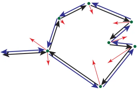
arrows) as a function of the in plane wave vector for Dresselhaus SO (a), linear Rashba SO (b) and cubic Rashba SO(c) . . . 34 3.3 Example of a self intersecting path inducing weak localization. When going
clockwise (black path) or counter clockwise (blue path) the charge carrier will experience the same momentum shifts (red arrows) on scattering centers (green dots) (thus getting the same phase accumulation) only when being back scattered. . . 37
List of figures xv
3.4 Schematic representing the electron spin rotation induced by traveling across a loop in one direction (⃗s →⃗s′) compared to traveling the opposite direction (⃗s →⃗s′′). Taken from [12] . . . 38 4.1 Left: Schematic of a Ge/Si core/shell nanowire showing the Ge core in
green and the Si shell in blue Right: Schematic of the radial band diagram of a Ge/Si core/shell nanowire. The offset of the valence band (VB) and conduction band (CB) creates a quantum well in the Ge core due to the relative position of the Fermi energy (Ef) . . . 44 4.2 Left: Scanning electron microscope image of an array of interdigital gates.
The gates are made of 5/15 nm of Ti/Au and have a 60 nm pitch Right: Scanning electron microscope image of the gate array after deposition of 12 nm of HfO2dielectric (center of the image) . . . 45 4.3 Image of a full 4 inches wafer after bonding pads deposition. This wafer
contains 128 different chips. . . 46 4.4 Left: Picture of the microscope and the nanomanipulator Right: Closer
image of the tungstene tip with the sample and the nanowire substrate . . . 47 4.5 Left: Scanning electron microscope image of a nanowire deposited across
the gates. These Ge/Si nanowires are approximately 20 nm of diameter and a few microns in length Right: Scanning electron microscope image of a finished device showing a wire contacted by two metal leads . . . 49 4.6 Schematic of the measured device. The nanowire (blue) lies on top of 5
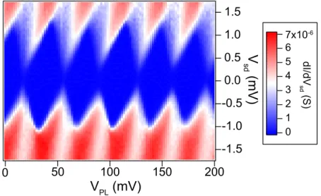
individual gates (green) and two sets of shorted gates (red) going under the Ni contacts (grey) . . . 50 4.7 Left: Current (I) as a function of source drain voltage (Vsd) in the full wire
with no voltage applied to any gate Right: Differential conductance (dI/dVsd) as a function of source drain voltage (Vsd) in the full wire with no voltage applied to any gate . . . 51 4.8 Differential conductance dI/dVsdas a function of PL gate voltage VP L
4.9 Differential conductance dI/dVsdin the wire as a function of PL gate voltage VP L and bias Vsd with no voltage applied on the other gates. The regular
shape and size of the Coulomb diamonds indicate a dot with a large number of charges . . . 53 4.10 Differential conductance dI/dVsdmeasurement of the wire as a function of
right (left graph) and left contact gates (right graph). The periodicity of the Coulomb peaks is different from sweeps of an individual gate . . . 54 4.11 Differential conductance dI/dVsdof the wire as a function of both the left and
right contact gate voltages VC Land VC Rrespectively, with a barrier created
in the middle of the wire by BM (VB M= 4 V) . . . 55
4.12 Stability diagram of the double dot system as a function of gates BL and BR. At lower gate voltage (a), the dots are confined between the middle barrier (BM) and the contacts. As the gate voltages are increased, the gates BR and BL start creating barriers (b) and the dots end up confined between the the middle barrier BM and the two side barriers BL and BR (c) . . . 56 4.13 Stability diagram of the studied double dot system, with the dots on top of
PL and PR. The red dashed box highlights the studied transition. . . 57 4.14 The same double triangle at different bias and magnetic field. a): VSD=4 mV
and no magnetic field. b): VSD=-4 mV and no magnetic field. c): VSD=4 mV and B = 2 T. d): VSD=4 mV and B= 4 T . . . 58
5.1 Schematic of the heterostructure used in this chapter. On a silicon wafer is deposited a buffer layer of SiGe. On top of this buffer layer, 32 nm of Ge are strained, thus inducing the formation of a 2DHG at the top surface . . . 62 5.2 a): Optical image of the surface of the heterostructure after etching of the
55 nm deep mesa.b): Optical image of the sample after deposition of the 60 nm Pt contacts.c): An oxide layer of 30 nm of Al2O3is deposited by ALD over the sample and a Ti/Au hall bar shaped accumulation top gate is evaporated on top.d): Zoom on the Hall bar shaped top gate . . . 64
List of figures xvii
5.3 Optical image of the Hall bar device. The blue line outlines the mesa and the white dashed lines the Pt contacts. We measure the Hall voltage (VH) and the channel voltage (Vch) from which we extract Hall resistivity and channel resistivity respectively. Direction of the two components for the applied magnetic fields is also indicated. . . 65 5.4 Channel resistivityρX X (red) and Hall resistivityρX Y (blue) as a function of
out of plane magnetic field B⊥. Channel resistivity shows a dip at low field which is a signature of weak antilocalization. . . 66 5.5 Mobilityµ (red) and carrier density nhol e (blue) as a function of
accumula-tion gate voltage . . . 67 5.6 Traces of the contribution of antilocalization on the channel conductivity
∆σW ALas a function of perpendicular magnetic field for different
accumula-tion gate voltages ranging from 1.3 × 1011cm−2(top trace) to 1.7 × 1011cm−2 (bottom trace). The antilocalization peaks disappears as carrier density is reduced (traces are offset for better visibility). . . 69 5.7 Evolution of scattering timeτt r (red crosses), phase relaxation timeτϕ(blue
circles) and spin relaxation timeτSO(blue triangles) as a function of carrier
density . . . 70 5.8 Evolution of the spin splitting energy∆SOas a function of carrier density . . 71
5.9 Black circles: quantum correction to channel conductivity∆σW ALas a
func-tion of in plane magnetic field. Fitting with the model from Minkov et al. [12] (blue dashed line) does not agree with our data without the addition of a B//6 (red line) term describing the virtual occupation of unoccupied subbands 72 5.10 Hall resistivity ρX Y as a function of in plane magnetic field. The small
dependance on field indicates a tilt of the sample of only 2◦. . . 73
6.1 Schematic of the heterostructure used in this chapter. On a silicon wafer is deposited a buffer layer of Si0.2Ge0.8. On top of this buffer layer, a 22 nm layer of Ge is deposited, then covered by 70 nm of Si0.2Ge0.8. Due to lattice mismatch the Ge layer is strained, thus inducing the formation of a 2DHG in it 81
6.2 Optical image of the Hall bar measured in this chapter. The points at which the channel bias Vchand the Hall bias VHare measured are also displayed . 82
6.3 Left: SEM image of the sample with added color showing the mesa (green), the ohmic contacts (red) and the bonding pads for the gates (blue, only three were connected to an actual gate) Right: Close SEM image showing the 300 nm wide constriction in the accumulation gate where the QPC is situated, as well as the two side gates situated at 70 nm of the constriction . . . 83 6.4 Hall resistivityρX Y (black) as well as channel resistivityρX X (red) as a
func-tion of magnetic field for Vt g= -3.9 V. The plateaus inρX Y and the oscillations
inρX X (Shubnikov-de Haas oscillations) are signatures of the quantum Hall
effect. No weak antilocalization is observed . . . 84 6.5 Mobilityµ (red crosses) as well as carrier density nhol e (blue circles) as a
function of accumulation gate Vt g . . . 85
6.6 Conductance G in the QPC as a function of gates voltage Vg showing
con-ductance steps of 2e2/h. On the rightmost step, a kink can be observed, also known as the 0.7 anomaly . . . 86 6.7 Traces of device conductance G as a function of gates voltage Vg for different
magnetic fields B applied (traces are offset horizontally for better visibility), starting at 0T (rightmost trace) to 0.5 T (leftmost trace) in steps of 0.1 T. As the magnetic field is increased, the 2e2/h steps split into e2/h steps due to Zeeman splitting of the subbands. . . 88 6.8 Differential conductance∂G/∂Vg as a function of gates voltage Vg and
mag-netic field B . The blue dashed lines highlight the position of the peaks that are synonym of steps in the conductance G . . . 89
List of figures xix
6.9 Differential conductance∂G/∂Vg a function of gates voltage Vg and source
drain bias Vsd for an out of plane magnetic field B of 0.5 T. The yellow
dashed lines highlight the position of peaks that are synonym of steps in the conductance G. These peaks form diamond shapes and the conductance is quantized inside them. The white numbers give the value of conductance in these plateaus in scale of e2/h. The red dashed line highlight the bias position of the tip of the 3e2/h diamond from which a g-factor of 19 is extracted. The black crosses highlight the gate splitting of the peak from which the gate lever arm is extracted. . . 90
List of tables
1.1 Natural isotopes, spin and natural abundance for most commonly used elements in spintronic . . . 11
Introduction
During the second half of the 20thcentury computers have revolutionized the way scientific research is made. The ever increasing computing power available allowed for the simulation of problems of exceptional complexity. Still, as Richard Feynman explained in his famous talk in 1981 [1], a classical computer, being limited to classical physics, will never be a universal computer, that is to say a computer that can be used to simulate any physics problem. In particular, being based on classical physics, classical computers could not properly simulate the quantum world. This would require a quantum computer.
In classical computing, information is encoded in bits. These bits are two levels sys-tems, usually denoted by 0 and 1. On chips, such as CPUs, they are physically implemented by transistors of which the open or closed status are the two levels of the bit. In a quantum computer, these classical bits would be replaced by quantum bits or qubits. Instead of a classical two level system, that can be 0 or 1, a qubit would rely on a quantum two level system, that can be in any superposition of the two levels.
Qubits can theoretically be realized with any quantum two level system, but a quantum computer should be based on qubits that respects the 5 DiVincenzo’s criteria exposed in 2000 [2]. In 1998 Loss and DiVincenzo had already made a proposal for such a system. The idea was to use the spin of an electron in a quantum dot as a two level system [3], thus providing an efficient way to do two qubits gates (one of DiVincenzo’s criteria) by the simple use of electrical gating.
This proposal led to an increase in interest in the field of quantum spintronic. Research was performed in order to engineer qubits in different systems, mainly III-V materials such as GaAs two dimensional electron gas [4] or InAs nanowires [5].
But not every qubit are equal. Indeed, in order to create a fault tolerant quantum computing system, one has to use quantum error correction codes [6] that require that the qubit states lifetimes are longer than the operation gate times. As the hyperfine interaction is the main reason for spin decoherence, more and more interest has been seen for group IV materials such as Ge and Si recently for which almost all natural isotopes have no nuclear spins.
The prospect of realizing a quantum computer based on spin qubits then require the use of a material in which spin manipulation is fast and coherence time is long. Systems based on strained germanium is expected to present such characteristics. The aim of this thesis is to present experiments that will tend to bring new information on the validity of these claims.
The outline of this thesis will be as follows. The first chapter will try to highlight the advantages of Germanium in the field of quantum spintronic, focusing around the low hyperfine interaction and strong spin orbit coupling. The second chapter focuses on the theory of quantum dots and double quantum dots systems. This chapter is limited to the concepts required for a correct understanding of the results obtained in the fol-lowing chapters, that is to say charging effect in quantum dots and double dots systems and Pauli spin blockade. Chapter three describes the theory of spin orbit interaction. Similarly to chapter two, this chapter does not pretend to be a review on spin orbit but only highlights the elements of this theory that permit to describe the systems described in the following chapters. In chapter four, experiments on Ge/Si core/shell nanowires are described. In these nanowire, a quantum dot form naturally due to contact Schottky barriers and is studied. By the use of electrostatic gates, a double dot system is formed and Pauli spin blockade is revealed. The fifth chapter reports magneto-transport mea-surements of a two-dimensional hole gas in a strained Ge/SiGe heterostructure with the quantum well laying at the surface, revealing weak antilocalization. By fitting quan-tum correction to magneto-conductivity characteristic transport times and spin splitting energy of 2D holes are extracted. Additionally, suppression of weak antilocalization by a magnetic field parallel to the quantum well is reported and this effect is attributed
LIST OF TABLES 3
to surface roughness and virtual occupation of unoccupied subbands. Finally, chapter number six reports measurements of quantization of conductance in strained Ge/SiGe heterostructure with a buried quantum well. First the heterostructure is characterized by means of magneto-conductance measurements in a Hall bar device. Then another device engineered specifically as a quantum point contact is measured and displays steps of conductance. Magnetic field dependence of these steps is measured and an estimation of the g-factor for heavy holes in germanium is extracted.
References
[1] Richard P. Feynman. Simulating physics with computers. International Journal of Theoretical Physics, 21(6):467–488, 1982.
[2] David P DiVincenzo et al. The physical implementation of quantum computation. arXiv preprint quant-ph/0002077, 2000.
[3] Daniel Loss and David P. DiVincenzo. Quantum computation with quantum dots. Phys. Rev. A, 57:120–126, Jan 1998.
[4] Sandra Foletti, Hendrik Bluhm, Diana Mahalu, Vladimir Umansky, and Amir Yacoby. Universal quantum control of two-electron spin quantum bits using dynamic nuclear polarization. Nature Physics, 5(12):903–908, 2009.
[5] S Nadj-Perge, SM Frolov, EPAM Bakkers, and Leo P Kouwenhoven. Spin-orbit qubit in a semiconductor nanowire. Nature, 468(7327):1084–1087, 2010.
[6] Simon J Devitt, William J Munro, and Kae Nemoto. Quantum error correction for beginners. Reports on Progress in Physics, 76(7):076001, 2013.
Chapter 1
Advantages of strained germanium for
quantum spintronics
The prospect of a quantum computer implies the realization of tens of coherently cou-pled quantum bits or qubits [1]. While creating a single qubit can already be challenging, fault-tolerant quantum computation requires that the qubits used possess high fidelity [2]. Each individual qubits can have a different fidelity and while some of the parameters influencing this fidelity are dependent on the type of qubit realized and the measurement setup, the host material for the qubit plays a large role in the gate control fidelity and defines the upper bound limit of the qubit fidelity.
It is possible to define a quality factor Q for a qubit representing its efficiency at gate control [3]. This quality factor Q = T2Rabi/Tπrepresents the ratio between the qubit decay time T2Rabi and theπ rotation time of the qubit quantum state. A higher Q factor then represents a higher probability of the response to a qubit manipulation to be coherent with the initial state.
Choosing a good host material for spin qubits is then of the utmost importance as the nature of the material will have a big impact on the quality factor. On theπ rotation time first as the presence of spin orbit interaction can help the manipulation of the spin by fully electrical control. On the qubit decay time T2Rabi then as the hyperfine interaction is the main reason for spin decoherence in quantum dots and is due to the presence of nuclear
spins in the host material. Germanium presents advantages in both parameters as will now be detailed.
1.1 Hyperfine interaction
When using the spin of an electron or a hole to encode quantum information, as in spin qubits, it is important that the spin maintains its phase for a duration long enough so that it can be manipulated or read and that the end state of this operation is coherent with the initial state. While in bulk semiconductors, charge carriers spin decoherence mainly occurs due to scattering through mechanism such as D’Yakonov-Perel [4], in quantum dots where charge carriers are confined, the main source of decoherence is the hyperfine interaction, that is to say the electron-nucleus spin interaction.
As opposed to an atom where the spin of an electron only interacts with the spin of its own nucleus through hyperfine coupling, in quantum dots, the spin of a charge carrier will interact with a lot of nuclei (N ≃ 105) and their spins (see Fig.:1.1a)[5]. The slow and random fluctuations of the effective magnetic field created by these nuclear spins (known as the Overhauser field) will in turn induce a random evolution of the charge carrier spin, thus inducing decoherence.
To the first order, the hyperfine interaction can be considered only as a Fermi contact hyperfine interaction whose Hamiltonian can be written as:
H =Xn
k
(Ak⃗Ik⃗S) (1.1)
Where ⃗Ik is the spin operator for the nucleus k and ⃗S the one for the charge carrier
spin. The term Akrepresents the coupling strength between the nucleus spin k and the
carrier spin, and is proportional to the square of the overlap of the nucleus and carrier k wavefunctions.
The first reason why strained Ge is so interesting as a host material for qubits with regards to hyperfine interaction comes from the nature of the charge carrier. While as of today most qubits experiments have been performed with electrons, intrinsic
compres-1.1. HYPERFINE INTERACTION 9
sively strained Ge, whether in core/shell nanowire or in two-dimensional heterostructures form holes quantum wells [6][7]. With regard to hyperfine interaction, the main advantage of holes as opposed to electrons comes from the overlap of their wavefunction with nuclei spin wavefunction. Electron conduction states are formed from atomic s orbitals, mean-ing that the amplitude of their wavefunction is larger at the location of the nuclei. On the other hand, holes conduction states are formed from atomic p orbital which amplitude is 0 at the location of the nuclei. This implies that the Fermi contact hyperfine interaction is equal to zero for conduction holes as the Akof the Hamiltonian are equal to zero.
Fig. 1.1:
a: The electron or hole wavefunction spatial extension covers around N ≃ 105atoms, interacting with their spins. b:Electron conduc-tion states are formed from atomic s orbitals of which the amplitude is localized on a unit cell. c: Holes conduction states are formed from atomic p orbital which amplitude is 0 at the location of the nuclei. From [5]With holes as charge carriers, the only influence of the hyperfine interaction on the carrier spin is through a dipole-dipole interaction between the carrier and nucleus spins. Conduction electrons are formed from s orbitals and dot not possess an angular momen-tum, thus they dot not have a dipole-dipole interaction with the nuclei spins. Conduction holes on the other hand are formed from p orbitals and have a non-zero angular
mo-mentum. Pure heavy holes for example have Jz= ±3/2. This will induce a dipole-dipole
interaction between the hole spin and the different nucleus spins. Still this interaction has been shown to be around 10 times weaker than the contact Fermi interaction of electrons [8], thus confirming that using holes as charge carriers is an advantage with regards to spin qubit coherence time.
When looking at the strength of the dipole-dipole interaction for holes or the Fermi contact interaction if electrons are used as charge carriers, germanium shows a second advantage over other standard spintronic materials and this advantage is related to the spin of the Ge nuclei. The only natural isotope of germanium with a non zero nuclear spin is73Ge (spin equal to 9/2) and has a natural abundance of only 7.73%. Looking back at equation 1.1 for the Fermi contact interaction for electrons in Ge, one can understand that with most of the ⃗Ikequal to zero, the interaction will be weaker than for another material
like GaAs where all isotopes of both elements have a non zero nuclear spin. Still, Ge is less attractive than Si in this regard as the only isotope with non zero nuclear spin is29Si (spin equal to 1/2) and has a natural abundance of only 4.68%. The same principles apply for the dipole-dipole interaction, which will be weaker in Ge than in other III-V materials but still stronger than in Si due in part to natural abundance but mostly due to the fact that a spin 9/2 will create a much stronger dipole than a spin 1/2. A summary of natural isotopes of the most commonly used elements for spintronic and their respective spins is given in table 1.1.
1.2 Spin orbit interaction in quantum dots
Spin qubits use the spin of a charge carrier as a two level system to encode quantum information [9]. To engineer such a qubit, it is then required to be able to drive coherently the spin between these two levels. One possible technique is Electron Spin Resonance or ESR which uses an oscillating magnetic field to induce coherent rotations of the spin state. Still, this technique presents some drawbacks. It usually requires a microfabricated ESR antenna, i.e. a conducting line close to the qubit, through which an oscillating current is
1.2. SPIN ORBIT INTERACTION IN QUANTUM DOTS 11
Element Isotope Spin Natural abundance (% atom)
Germanium 70Ge 0 20.84 72Ge 0 27.54 73Ge 9/2 7.73 74Ge 0 36.28 76Ge 0 7.61 Silicon 28Si 0 92.23 29Si 1/2 4.68 30Si 0 3.09 Gallium 69Ga 3/2 60.10 71Ga 3/2 39.90 Indium 113In 9/2 4.29 115In 9/2 95.71 Arsenic 75As 3/2 100 Antimony 121Sb 5/2 57.21 123Sb 7/2 42.79
Table 1.1:
Natural isotopes, spin and natural abundance for most commonly used elements in spintronicdriven, thus generating an oscillating magnetic field. Due to Joule heating, this technique cannot allow for fast rotation of the spin, which in turns leads to low qubit fidelity.
In a sample where charge carriers experience spin orbit interaction, a second possibil-ity arises. Indeed, spin orbit interaction, as will be detailed in chapter 3, links the spin of a particle to its orbital motion. In a quantum dot, due to the little amount of space available for the charge carriers to move in, one may expect spin orbit interaction to have a limited effect. While it is definitely different from the effect observed in bulk materials, the spin orbit interaction affects the spins of confined particles in a quantum dot by mixing the pure spin states | ↑ 〉 and | ↓ 〉. The eigenstates are then admixtures of spin and orbital degrees of freedom.
This is a significant change as an electric field cannot induce transitions between pure spin states, but it can for these mixed states. One can then produce an oscillating electric field on a quantum dot rather than a magnetic field and then drive the spin of a charge carrier from one state to the other. This spin control technique called Electrically Driven Spin Resonance or EDSR is far more efficient than ESR in terms of potential spin rotation time.
A strong spin orbit interaction can also have drawbacks for a qubit though. While it allows for faster qubit manipulation, thus shorter Tπ, a strong mixing of the pure spin states | ↑ 〉 and | ↓ 〉 can make the system sensitive to charge fluctuation in its environment such as electrostatic gate noise, thereby leading to shorter decay time T2Rabi. This is why it is still relevant to perform research toward new materials for quantum spintronics, in order to find a material with the most effective balance between pros and cons. Germanium could be this material as it is known to show spin orbit interaction [10].
References
[1] David P DiVincenzo et al. The physical implementation of quantum computation. arXiv preprint quant-ph/0002077, 2000.
[2] Emanuel Knill. Quantum computing with realistically noisy devices. Nature, 434(7029):39–44, 2005.
[3] Kenta Takeda, Jun Kamioka, Tomohiro Otsuka, Jun Yoneda, Takashi Nakajima, Matthieu R. Delbecq, Shinichi Amaha, Giles Allison, Tetsuo Kodera, Shunri Oda, and Seigo Tarucha. A fault-tolerant addressable spin qubit in a natural silicon quan-tum dot. Science Advances, 2(8), 2016.
[4] MI Dyakonov and VI Perel. Spin relaxation of conduction electrons in noncentrosym-metric semiconductors. Soviet Physics Solid State, Ussr, 13(12):3023–3026, 1972.
[5] Richard J Warburton. Single spins in self-assembled quantum dots. Nature materials, 12(6):483–493, 2013.
[6] Wei Lu, Jie Xiang, Brian P Timko, Yue Wu, and Charles M Lieber. One-dimensional hole gas in germanium/silicon nanowire heterostructures. Proceedings of the Na-tional Academy of Sciences of the United States of America, 102(29):10046–10051, 2005.
[7] Rai Moriya, Kentarou Sawano, Yusuke Hoshi, Satoru Masubuchi, Yasuhiro Shiraki, Andreas Wild, Christian Neumann, Gerhard Abstreiter, Dominique Bougeard, Takaaki Koga, and Tomoki Machida. Cubic rashba spin-orbit interaction of a two-dimensional
hole gas in a strained-ge/sige quantum well. Physical review letters, 113(8):086601, 2014.
[8] Christophe Testelin, Frédéric Bernardot, Benoît Eble, and Maria Chamarro. Hole– spin dephasing time associated with hyperfine interaction in quantum dots. Physical Review B, 79(19):195440, 2009.
[9] Daniel Loss and David P. DiVincenzo. Quantum computation with quantum dots. Phys. Rev. A, 57:120–126, Jan 1998.
[10] Christopher Morrison, Jamie Foronda, P Wi´sniewski, SD Rhead, David R Leadley, and Maksym Myronov. Evidence of strong spin–orbit interaction in strained epitaxial germanium. Thin Solid Films, 602:84–89, 2016.
Chapter 2
Quantum dots and double dots systems
In electronic transport in semiconductors, one of the basic system that can be fab-ricated is a quantum dot. In these elements the quantification of charge plays a very important role in the transport characteristics, allowing them to be used as blocks of a more complex device to perform charge sensing, electronic thermometry or spin readout for example. In this section, the physics behind quantum dots and double dot systems as well as the experimental evidences of these properties in electronic transport are explained in the scope of the work performed in this thesis.
2.1 Quantum dots
2.1.1 Device geometry
In order to engineer a quantum dot for electronic transport, one has to isolate a small section of a bigger semiconductor system. This is usually done in nanowires or two-dimensional electron/hole gases as will be shown in this thesis or in semiconductor islands such as self assembled quantum dots [1]. Tunnel barriers are used for separation from the rest of the system in order to allow for charge transport across the dot as required for transport experiments. These barriers can be created by electrostatic gating [2] or by
materials interfaces [3]. The quantum dot is usually connected to one or several gates called plunger gates in order to modify the electrostatic potential of the dot [4].
V
SDV
gI
Fig. 2.1:
Schematic of a quantum dot (red) connected to the rest of the system by leads (blue) through tunnel barriers (green). Transport experiment are usually done by applying voltage on the source (VSD) and measuring the current (I) going through. The chemical potential of the dot can be changed by applying a voltage (Vg) on a plunger gate (maroon)2.1.2 Charging energy
In a quantum dot such as the one described previously, adding an electron requires an additional energy, or charging energy [5]. This energy consists in two phenomena. The first one, which is not exclusive to quantum dots is the coulombian repulsion term [6]. Charge carriers, whether they are electrons or holes are charged particles. In a small island of a metal or semiconductor, they will repel each other. This is why adding another charge will require an additional energy to counter this repulsion. This term will be equal to e2/C where C is the total capacitance of the island to its environment. This phenomenon is the one behind the functioning of single electron transistors (SET) [7].
The second phenomena is at the essence of a quantum dot. Such a system has to be small enough so that the charge carriers have a deBroglie wavelength of approximately the
2.1. QUANTUM DOTS 17
same size as the dot, meaning the maximum dot size is dependent on the material used (through the effective mass of the charge carrier). This implies that the charge carriers occupy discrete quantum levels that have a discrete energy spectrum (properties for which they are sometimes referred to as artificial atoms) [8]. This discrete energy spectrum is the reason why adding a charge carrier to a dot requires a second additional energy (that we will refer to as orbital spacing). The smaller the dot and the number of charge carriers in it, the bigger this orbital spacing term.
2.1.3 Coulomb peaks
When connecting a quantum dot to two reservoirs via tunnel barriers, charge carriers will tunnel in the dot in order to minimize the energy of the system. When no bias is applied across the dot, the levels of the reservoirs are aligned. As tunneling through a tunnel barrier is only allowed when the end level is aligned with the starting level, charge transport across the dot is only possible when the first available state in the dot is aligned with the reservoirs. In this configuration both the states with N and N+1 charges in the dot are possible where N is the total number of charge in the dot. When modifying the voltage applied on the plunger gate by∆Vg, the potential of the dot is changed by
∆µd ot= αg× ∆Vg whereαg is the lever arm of the gate on the dot (αg= Cg/C where Cg
is the capacitance of the plunger gate to the dot). By linearly sweeping the plunger gate, one can switch the quantum dot from off to on for discrete values of Vg, when a level of
the dot aligns with the leads. Probing the dot conductivity as a function of gate voltage will result in series of peaks called Coulomb peaks. In between these peaks, the system is blocked and the number of charge inside the dot is perfectly defined.[5]
As the Coulomb peaks appear when a dot level is aligned with the reservoirs Fermi energy, it is possible to extract the charging energy of the dot from the peak spacing via the formula∆EN →N +1= αg× ∆Vg ,N →N +1. When the dot is filled with a high number of
charges, the coulombian repulsion term in the charging energy (e2/C where C is the total capacitance of the dot to its environment) is dominant compared to the orbital
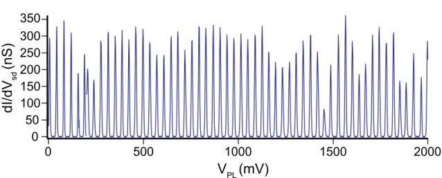
spacing of the dot. That leads to Coulomb peaks with highly regular spacing equal to ∆Vg = ∆E/αg= e2/αgC (see fig. 2.2).
350 300 250 200 150 100 50 0 2000 1500 1000 500 0
V
PL(mV)
dI/dV
sd(nS)
Fig. 2.2:
A series of highly regularly spaced Coulomb peaks. Data from chapter 4When the number of charges in the dot becomes smaller, the orbital spacing of the dot levels reaches the same order of magnitude as the coulombian repulsion energy, creating a difference between odd and even filling of the dot. When the dot is filled with an odd number of charges, adding one more will only require the coulombian energy as the new charge will occupy an orbital level already containing the previous charge. On the other hand, when adding a charge to a dot filled with an even number of charges, the required energy will be the coulombian term plus the orbital energy spacing between the last orbital level filled and the one the new charge will occupy.
When reaching the last few charges in a dot, the charging energy tends to increase a lot from one transition to the other. This is mainly due to two mechanisms. The first one is that the orbital spacing will continue increasing as the number of charges gets smaller, thus increasing the charging energy. The second reason is due to the fact that when reaching a low number of charges by the use of a gate, the electrical field created by the plunger will also modify the shape of the dot. This will lead to a modification of C the total capacitance of the dot and of the gate lever armαg, leading to a change in
2.1. QUANTUM DOTS 19
energy of a dot with a low number of charge, one has to perform bias spectroscopy of the dot.
2.1.4 Coulomb diamonds
When applying a voltage VSDbetween source and drain, an energy difference qVSD will be created between the two reservoirs. From now on we will consider that the charge carriers are holes, meaning that q is equal to e and not −e as it would be for electrons. It means that in our case, for a positive bias, the holes in the source lead are of higher energy than the ones in the drain lead.
While with no bias applied the dot was in an on state only when a level was aligned with both contacts, it is now on whenever a level gets an energy situated in between the Fermi energies of the leads. When looking at the conductance of the dot as a function of gate voltage, what were previously peaks will then widen linearly and become plateaus as a function of bias as w = αgVSDwhere w is the plateau width. Measuring the current going
through a quantum dot as a function of both gate voltage and bias will display distinctive features called Coulomb diamonds as the off region of the dot gets smaller as the bias gets higher (see fig. 2.3
200 150 100 50 0 -1.5 -1.0 -0.5 0.0 0.5 1.0 1.5 7x10⁻⁶ 6 5 4 3 2 1 0
V
PL(mV)
V
sd(mV)
dI/dV sd (S)Fig. 2.3:
Conductance of a dot as a function of bias and gate voltage. Data from chapter 4With high enough bias, the dot will be in an on configuration for all gate voltage values. This happens when the bias window is big enough so that it becomes higher than the splitting between two levels of the dot, thus ensuring that at least one level will always be in the bias window regardless of the gate voltage. It allows for charging energy extraction from the Coulomb diamonds as the tip of a diamond represents the exact bias for which two dot levels enter the bias window, that is to say that eVSDis equal to the charging energy to go from one of these levels to the other.
2.2 Double dot systems
In order to perform a spin qubit, one has to readout the quantum state of the spin of a single charge carrier. The magnetic moment of a single spin being so weak, it is extremely difficult to perform its electrical readout directly [9]. To counter this difficulty, it is possible to conceive charge transport processes that are spin selective, that is to say to perform spin to charge conversion. It is then easier to measure charge than spin. The most common process used relies on Pauli spin blockade and requires two quantum dots in series, a system whose physics will now be detailed.
2.2.1 Stability diagram
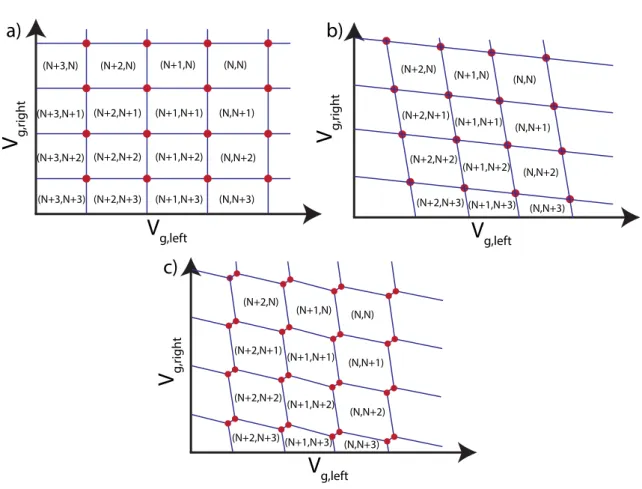
The stability diagram of a double dot system represents the charge configuration of the dots as a function of both gates voltage. The experimental depiction of this diagram is the measurement of the conductivity of the double dot system as a function of gates voltage. For a system made of two quantum dots in series to be conductive, both of the dots must be in an on state at the same time. A simplistic representation of this would be to first consider both dots independently with their own conductance resonances, and just consider that the system will be conducting when both gate voltages will attain the values of resonance, as depicted on fig 2.4 a.
This picture is only true for completely decoupled quantum dots. When the two dots are close enough, there is a cross capacitance of the gates, meaning that varying the gate
2.2. DOUBLE DOT SYSTEMS 21
voltage of one dot will also vary the energy levels of the other dot. This implies that the voltages at which each dot gets its resonances will not be constant but will vary linearly with the gate voltage of the other dot, as shown in fig 2.4 b.
The most important difference between this first approach to a stability diagram and the reality of coupled quantum dots is the separation of the resonances. Each of the resonances depicted before are actually split into two resonances in a coupled double dot system and the diamond shaped regions where charge configurations are defined turn into hexagons (see fig 2.4 c). This has to be explained by a charging energy of the whole system. Resonances are points in the stability diagram where several charge configuration are favorable, thus allowing charges to go across the system. Splitting of the resonances in a coupled double dot system is the evidence that is not possible to go straight from a (N1,N2) charge configuration to a (N1+1,N2+1) (where Niis the charge number in the dot i). One could imagine that such a change in charge configuration would be possible if both the dots and contacts levels were aligned, but then adding a charge to one of the two dots would lift the level of the second one, due to the cross capacitance. Additional gate voltage would then be required for a charge to enter the second dot.
Each of the resonances is then a gate configuration where three charge configura-tions of the charge system are accessible, explaining why they are sometimes referred to as triple points. This allows for charge transfer across the system through a cycle of the type (N1,N2)→(N1+1,N2)→(N1,N2+1)→(N1,N2) or (N1,N2+1)→(N1+1,N2+1)→(N1+1,N2)→(N1,N2+1), thus making the double dot system conducting.
While technically challenging [10], for spin qubit engineering, it is usually useful to use the stability diagram to set the system on the triple point with the lowest number of charges. While the physics behind quantum dot levels and spin and charges interaction is well understood for few charges systems, systems with higher number of charges can be hard to describe and tune precisely [11].
V
g,leftV
g,r igh tV
g,leftV
g,r igh t (N,N) (N,N+1) (N,N+2) (N,N+3) (N+1,N) (N+1,N+1) (N+1,N+2) (N+1,N+3) (N+2,N) (N+2,N+1) (N+2,N+2) (N+2,N+3) (N+3,N) (N+3,N+1) (N+3,N+2) (N+3,N+3) (N,N) (N,N+1) (N,N+2) (N,N+3) (N+1,N) (N+1,N+1) (N+1,N+2) (N+1,N+3) (N+2,N) (N+2,N+1) (N+2,N+2) (N+2,N+3)V
g,leftV
g,r igh t (N,N) (N,N+1) (N,N+2) (N,N+3) (N+1,N) (N+1,N+1) (N+1,N+2) (N+1,N+3) (N+2,N) (N+2,N+1) (N+2,N+2) (N+2,N+3)a)
b)
c)
Fig. 2.4:
Schematic of the stability diagram of a double dot system. a) Case with no coupling between the two dots. b) Cross capacitance of the plungers of the two dots is now taken into account. c) Coupling between the two dots splits each resonance into two triple points2.2.2 Conductance resonances characteristics
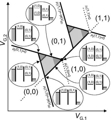
In the previous section, no bias was considered across the system. Since source and drain Fermi levels are aligned, resonances only appear for discrete values of gate voltages. When bias is applied between source and drain, it opens windows of conductance. The formerly point-like resonances will then turn into triangles.
As the bias is increased, the triangles get bigger. With high enough bias, there will be gate voltage values for which not only the ground state of a dot level is in the bias window but also one or more excited state. This will increase the conductance of the system as more levels are available for tunneling. In a conductance triangle, the position of the increase of conductance allows for excited states energy reading [12].
2.2. DOUBLE DOT SYSTEMS 23
Fig. 2.5:
Schematic of a double triangle resonance (for an electron double dot), showing the dots levels configuration for each features of the triangles. From [13].2.2.3 Pauli spin blockade
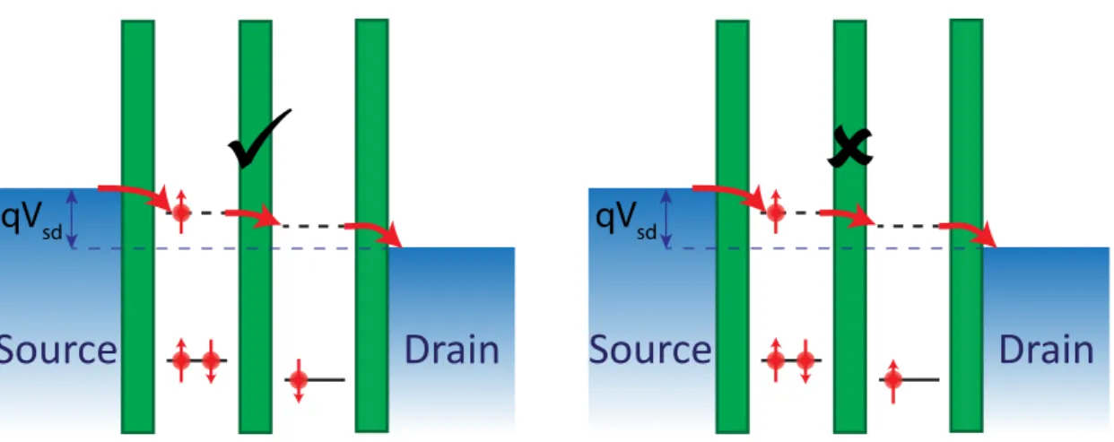
Until now, only spinless charge carriers were considered, but holes and electrons have a spin 3/2 and 1/2 respectively, leading to interesting phenomena on conduction in the presence of magnetic field due to Pauli exclusion principle. Let us now consider for example the charge triple point where transport through the double dot is done through the cycle (0,1)→(1,1)→(0,2)→(0,1). Let us also consider an external magnetic field applied on the system. This will lift the degeneracy between the spin up (| ↑ 〉) and spin down (| ↓ 〉) states of the dots.
Considering the transport cycle mentioned earlier, a hole will first enter the left dot. There is no selection of the hole leaving the lead with regard to its spin as it enters the dot on a new orbital. It will then try to tunnel to the right dot on an orbital where a hole is already present, leading to two possible scenarios. Either the hole on the left dot has its spin opposite to the one of the hole in the right dot. It will then be allowed to tunnel to
the right dot as they will form a spin singlet and will continue the cycle. Either the hole as the same spin direction as the one in the right dot. It will then not be allowed to tunnel to the right where it should form a spin triplet on the orbital which is not permitted due to Pauli exclusion principle. The hole will not be able to go back to the lead either as it has an energy lower that the Fermi level of the lead. Transport is then blocked in the system. This phenomena is called Pauli spin blockade.
qV
sdSource
Drain
qV
sdSource
Drain
Fig. 2.6:
Schematic representing the conditions in which spin selec-tivity in a double dot system can induce suppression of current. This phenomena is called Pauli spin blockade.If the bias is reversed, then Pauli spin blockade is suppressed. Indeed, the conduction cycle of the holes becomes (0,1)→(0,2)→(1,1)→(0,1). Here, blockade doesn’t happen as there will always be a hole in the right lead with the correct spin direction to enter the right dot. Any of the two holes in the right dot will then be able to tunnel to the left dot and then to the left lead, thus restarting the cycle.
Not all triple points meet the conditions to observe Pauli spin blockade. For example the triple point for which conduction involves the cycle (0,1)→(1,1)→(1,0)→(0,1) will not have spin blockade as it does not involve spin selectivity. Spin selectivity only occur when the cycle involves a transition (N1+1,N2+1)→(N1,N2+2) or (N1+1,N2+1)→(N1+2,N2) where N1and N2are even numbers of charge. It can be shown that this spin selectivity can occur for only one fourth of the triple points for a given bias direction and for another fourth of
2.2. DOUBLE DOT SYSTEMS 25
Fig. 2.7:
Schematic for two opposing biases of a double sot system. Pauli spin blockade appears for positive bias, but disappear when the bias is reversed.the triple points for the opposite bias direction. It is also to be noted that the Pauli spin blockade conditions for a bias direction are met for both triple points of a pair of triangles if they are met for one of them.
Experimentally, when Pauli spin blockade occurs, triangle resonances are usually not fully suppressed. It can happen that some edges of the pair of triangles are still visible. It represents the configuration when the level of the first dot is aligned with the Fermi level. There, when a hole with the wrong spin enters the first dot, it will not be able to tunnel through the system, but can go back to the lead. This cycle will happen until a hole with the right spin enters the dot and tunnels through the system (see fig 2.8 a). Another possibility is that only a region at the base of the triangles disappears due to Pauli spin blockade. This happens when the bias applied is high enough so that the triplet state of the (0,2) configuration becomes available for transport through the system. When magnetic field is applied, current is suppressed over the region (adjacent to the base) where tunneling can only occur through the singlet of (0,2), the triplet state of (0,2) being energetically inaccessible (see fig 2.8 b).
a)
b)
Fig. 2.8:
Experimental evidences of Pauli spin blockade. a) Only the edges of the pair of triangle still conduct (from [14]). b) Current is suppressed in a region near the base of the triangles. The extension of this spin blockaded region measured along the level detuning direction (perpendicular to the base) is set by the energy splitting∆ST betweenReferences
[1] N Ares, G Katsaros, VN Golovach, JJ Zhang, A Prager, LI Glazman, OG Schmidt, and S De Franceschi. Sige quantum dots for fast hole spin rabi oscillations. Applied Physics Letters, 103(26):263113, 2013.
[2] Carina Fasth, Andreas Fuhrer, Mikael T Björk, and Lars Samuelson. Tunable double quantum dots in inas nanowires defined by local gate electrodes. Nano letters, 5(7):1487–1490, 2005.
[3] Mikael T. Björk, Claes Thelander, Adam E. Hansen, Linus E. Jensen, Magnus W. Larsson, L. Reine Wallenberg, and Lars Samuelson. Few-electron quantum dots in nanowires. Nano Letters, 4(9):1621–1625, 2004.
[4] J. R. Petta, A. C. Johnson, J. M. Taylor, E. A. Laird, A. Yacoby, M. D. Lukin, C. M. Marcus, M. P. Hanson, and A. C. Gossard. Coherent manipulation of coupled electron spins in semiconductor quantum dots. Science, 309(5744):2180–2184, 2005.
[5] Leo P Kouwenhoven, Charles M Marcus, Paul L McEuen, Seigo Tarucha, Robert M Westervelt, and Ned S Wingreen. Electron transport in quantum dots. In Mesoscopic electron transport, pages 105–214. Springer, 1997.
[6] HR Zeller and I Giaever. Tunneling, zero-bias anomalies, and small superconductors. Physical Review, 181(2):789, 1969.
[7] Marc A Kastner. The single-electron transistor. Reviews of Modern Physics, 64(3):849, 1992.
[8] RC Ashoori, HL Stormer, JS Weiner, LN Pfeiffer, SJ Pearton, KW Baldwin, and KW West. Single-electron capacitance spectroscopy of discrete quantum levels. Physical review letters, 68(20):3088, 1992.
[9] JM Elzerman, R Hanson, LH Willems Van Beveren, B Witkamp, LMK Vandersypen, and Leo P Kouwenhoven. Single-shot read-out of an individual electron spin in a quantum dot. nature, 430(6998):431–435, 2004.
[10] J. M. Elzerman, R. Hanson, J. S. Greidanus, L. H. Willems van Beveren, S. De Franceschi, L. M. K. Vandersypen, S. Tarucha, and L. P. Kouwenhoven. Few-electron quantum dot circuit with integrated charge read out. Phys. Rev. B, 67:161308, Apr 2003.
[11] R. C. Ashoori, H. L. Stormer, J. S. Weiner, L. N. Pfeiffer, K. W. Baldwin, and K. W. West. N. Phys. Rev. Lett., 71:613–616, Jul 1993.
[12] W. G. van der Wiel, S. De Franceschi, J. M. Elzerman, T. Fujisawa, S. Tarucha, and L. P. Kouwenhoven. Electron transport through double quantum dots. Rev. Mod. Phys., 75:1–22, Dec 2002.
[13] R Hanson, LP Kouwenhoven, JR Petta, Seigo Tarucha, and LMK Vandersypen. Spins in few-electron quantum dots. Reviews of Modern Physics, 79(4):1217, 2007.
[14] A. C. Johnson, J. R. Petta, C. M. Marcus, M. P. Hanson, and A. C. Gossard. Singlet-triplet spin blockade and charge sensing in a few-electron double quantum dot. Phys. Rev. B, 72:165308, Oct 2005.
[15] Ruoyu Li, Fay E. Hudson, Andrew S. Dzurak, and Alexander R. Hamilton. Pauli spin blockade of heavy holes in a silicon double quantum dot. Nano Letters, 15(11):7314– 7318, 2015. PMID: 26434407.
Chapter 3
Spin orbit interaction
The spin orbit interaction (SOI) is one of the reasons why germanium is an interesting material for spintronic. In this chapter the physics of this interaction will be detailed, from its nuclear origin to the ability it provides to control electrically the spin of a charge carrier in a quantum dot.
3.1 Origin of spin orbit interaction
The SOI represents the coupling between the spin of an electron and its motion (its momentum), and can be treated as the effect of an effective ⃗k-dependent magnetic field. For proper treatment of the SOI, one has to derive the Dirac equation, but it is possible to describe it as a relativistic correction to the Schrödinger equation as will now be done here.
A moving electron, orbiting around its nucleus or diffusing in a lattice, is a charged particle moving in an electric field. We can consider it as a reference frame (the electron rest frame) moving at a speed⃗v relative to an electric field ⃗E. Following classical electrody-namics, this will induce an effective magnetic field in the electron rest frame that can be written as: ⃗ B = −1 c⃗v × ⃗E = 1 mc(⃗E × ⃗p) (3.1)
The electron, due to its magnetic moment⃗µ, will then acquire an energy:
−⃗µ.⃗B = −γ⃗s.⃗B = − γ
mc⃗s.(⃗E × ⃗p) (3.2)
Whereγ is the gyromagnetic ratio and⃗s the electron spin. Due to our assumption on the spin orbit (SO) term as a relativistic correction, this term is not fully correct and a full relativistic calculation would reveal a 1/2 pre-factor known as Thomas factor [1].
As can be seen from formula 3.2, an electron in an electric field will acquire an energy linked to its spin and its momentum. It can also be seen that this energy is dependent on the form of the electric field, whether it is the field created by the nucleus around which the electron orbits, the field created by the crystal in which the electron travels, the asymmetry of the lattice cell or the asymmetry of the confinement potential. For these reasons, SOI can have quite different consequences depending on the system studied. The effects of SOI for our system of choice will now be detailed.
3.2 Spin orbit interaction effect on band diagram
Here we will now describe the consequences of SOI for our specific system, that is to say a two-dimensional hole gas (2DHG) in a germanium heterostructure. The effects of SOI in the case of a Ge/Si core/shell nanowire will not be detailed here as SOI had little to none influence on the experiments on this system described in this thesis. Still, a full derivation of SOI in this system can be found in a paper by Kloeffel et al. [2].
The first effect of SOI on our system of interest comes from the atomic SOI. Indeed, in an atom, negatively charged electrons orbit around their nucleus. But in the rest frame of the electron, the nucleus is a positive charge orbiting the electron. This will induce an electric field highly influenced from the orbit of the electron (SOI takes its name from this specific consideration). Specifically, it is possible to show that the SO energy is linked to the product s.l where s is the spin of the electron and l its orbital momentum. This is of significant importance for our system, because in an electronic system, in a tight binding approach, electrons are described by s-like orbitals, for which the orbital momentum l
3.3. RASHBA SPIN ORBIT INTERACTION 31
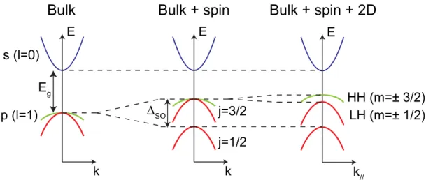
is equal to zero. Holes on the other hand are described by p-like orbitals, that is to say l = 1. Their total angular momentum j can then have two different values, j = 3/2 and j = 1/2. In this situation, it can be shown that the atomic SOI will split these two subbands by an energy gap∆0called the spin orbit gap. In germanium, the spin orbit gap has been measured and a value of∆0= 0.29 eV has been obtained [3]. The j = 1/2 subband, of lower energy than the j = 3/2 one, is usually called the split-off band.
Additionally, it can be shown that the j = 3/2 subband splits again for a non zero wavevector k into two subbands. Indeed when the quantization axis of the angular momentum ⃗j is chosen parallel to ⃗k, SOI interaction will induce a k dependent splitting between the m = ±3/2 states (called Heavy Hole states HH) and the m = ±1/2 states (Light Hole states LH) (see Fig.3.1).
Finally, in a two dimensional system, confinement will have an additional effect on the energy band diagram. Indeed, the projection of the electronic states in a 2DHG on the direction perpendicular to the quantum well (QW) corresponds to standing waves. This implies that even for an in-plane wave vector k//equal to zero, the total wave vector k is not zero, leading to a splitting of the HH and LH states even at k//= 0. This is for this reason that for low enough carrier densities, as it is the case in the experiments described in the next chapters, only the HH subband is occupied.
3.3 Rashba spin orbit interaction
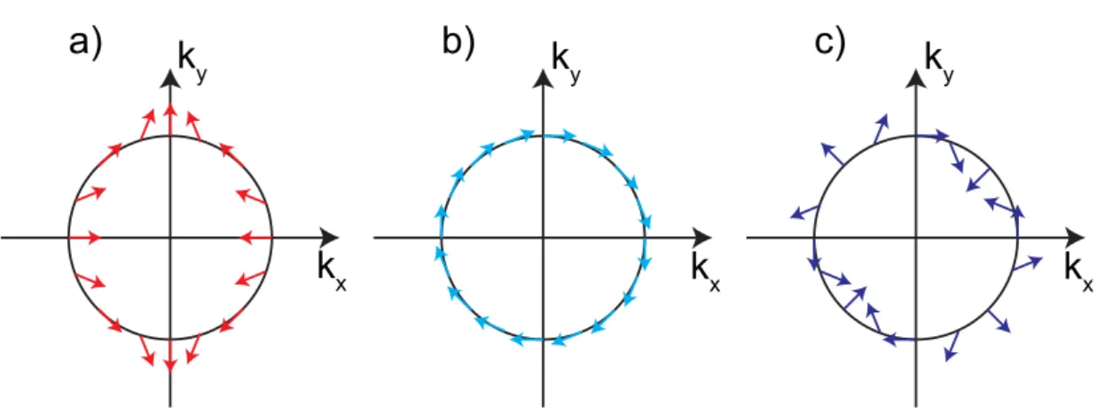
Spin orbit interaction can also lift the spin degeneracy of subbands when the charge carrier travels in a solid with spatial inversion asymmetry. In two-dimensional systems, it exists two main phenomena that can break space reversal symmetry. The first one is known as bulk inversion asymmetry (BIA) and is responsible for Dresselhaus SO. This is of little interest for us as BIA is a consequence of the absence of inversion center in the crystal structure, which is not the case for germanium (BIA is particularly relevant for III-V materials such as GaAs). The Dresselhaus HamiltonianHD contains both a k-linear and
E
k
E
k
E
k
//E
g∆
SOs (l=0)
p (l=1)
j=3/2
j=1/2
HH (m=± 3/2)
LH (m=± 1/2)
Bulk
Bulk + spin
Bulk + spin + 2D
Fig. 3.1:
left: Schematic of the energy band diagram for a bulksemi-conductor. The valence and conduction bands are separated by the band gap Eg. The electrons are described by s-like orbitals (l = 0) while
the holes are described by p-like orbitals (l = 1) center: Now taking into account spin, the SOI splits the valence band between the j = 3/2 states and the j = 1/2 states by a spin orbit gap ∆0right: In a 2DHG,
quantiza-tion in a direcquantiza-tion perpendicular to the QW plane leads to a splitting of the HH and LH states, even at k//= 0. Inspired from Winkler et al. and Moriya et al. [4, 5]
compared to the k-linear ones. Considering a basis x, y and z pointing along the main crystallographic direction (100), (010) and (001) respectively, and a 2D quantum well perpendicular to the (001) direction, this Dresselhaus Hamiltonian can be written as [6]:
HD= β£−kxσx+ kyσy
¤
(3.3)
whereβ is a pre-factor depending on material and confinement and σi represents
the Pauli matrices. It is often interesting to write this Hamiltonian as a Zeeman term HD = 12B⃗D(⃗k//) ·⃗σ, with ⃗BD(⃗k//) = 2β(−kx, ky). The direction of the effective field ⃗BD
created by the Dresselhaus SOI is represented in Fig.3.2a.
The second phenomena breaking space reversal symmetry is the structural inversion asymmetry (SIA) and is responsible for Rashba SO [7]. This type of SOI is the one to consider for a germanium 2DHG as it can be caused by an asymmetry of the confinement
![Fig. 2.8: Experimental evidences of Pauli spin blockade. a) Only the edges of the pair of triangle still conduct (from [14])](https://thumb-eu.123doks.com/thumbv2/123doknet/12848835.367778/49.892.118.761.445.676/fig-experimental-evidences-pauli-blockade-edges-triangle-conduct.webp)