HAL Id: hal-01217787
https://hal.archives-ouvertes.fr/hal-01217787
Submitted on 22 Oct 2015
HAL is a multi-disciplinary open access
archive for the deposit and dissemination of
sci-entific research documents, whether they are
pub-lished or not. The documents may come from
teaching and research institutions in France or
abroad, or from public or private research centers.
L’archive ouverte pluridisciplinaire HAL, est
destinée au dépôt et à la diffusion de documents
scientifiques de niveau recherche, publiés ou non,
émanant des établissements d’enseignement et de
recherche français ou étrangers, des laboratoires
publics ou privés.
Sub-Threshold Startup Charge Pump using Depletion
MOSFET for a low-Voltage Harvesting Application
Gaël Pillonnet, Thomas Martinez
To cite this version:
Gaël Pillonnet, Thomas Martinez. Sub-Threshold Startup Charge Pump using Depletion MOSFET
for a low-Voltage Harvesting Application. IEEE Energy Conversion Congress and Exposition, Sep
2015, Montréal, Canada. �hal-01217787�
Sub-Threshold Startup Charge Pump
using Depletion MOSFET
for a low-Voltage Harvesting Application
Gaël Pillonnet
1, Thomas Martinez
1,21 Univ. Grenoble Alpes, F-38000 Grenoble, France, and CEA, LETI, MINATEC Campus, F-38054 Grenoble, France 2
École polytechnique, Département de Physique, 91128 Palaiseau, France
Abstract— This paper presents a fully integrated CMOS
start-up circuit for a low voltage battery-less harvesting application. The proposed topology is based on a step-up charge pump using depletion transistors instead of enhancement transistors. With this architecture, we can obtain a self-starting voltage below the enhancement transistor’s threshold due to its normally-on operation. The key advantages are the CMOS compatibility, inductor-less solution and no extra post-fabrication processing. The topology has been simulated in 0.18µm technology using a transistor-level model and has been compared to the traditional charge pump structure. The depletion-based voltage doubler charge pump enables operation from an input voltage as low as 250mV compared to 400mV in an enhancement-based one. The proposed topology can also achieve other conversion ratios such as 1:-1 inverter or 1:N step-up.
Keywords— DC-DC converter, charge pump, low-voltage startup, depletion MOSFET, energy harvesting interface, thermo-energy generator.
I. INTRODUCTION
Ambient energy scavenging has become a key alternative to conventional batteries leading to self-powered devices and allowing maintenance-free operation of electronic devices especially wireless sensor nodes [1]. It solves the problem of battery lifetime by harvesting thermal, solar, chemical or mechanical energy directly from the system environment. Among those possibilities, thermo-electric generators (TEGs) exploit a temperature gradient to provide electric energy and are pertinent solutions for numerous applications which consume less than a few mW.
Due to the low temperature gradient in most applications, the TEG only delivers a DC voltage of a few hundred millivolts. The TEG output has to be adapted by a harvesting circuit in order to extract [12], step up the voltage and obtain a sufficient voltage in order to charge a battery or to directly power a sensor node. Due to the low power generated by the TEG, both extraction and conversion steps have to be achieved at the best power efficiency.
Another harvester circuit constraint is the “cold start” i.e. without initial energy when the battery is completely discharged. The harvester circuit therefore has to self-start with only the low voltage delivered by the TEG. The low-voltage cold-start (below 300mV) is a key bottleneck in the harvesting
circuit design leading to an increase in size and startup time. This paper will address this key issue.
Several low-input voltage converters have been published in the literature. Some systems [12, 16] use an initial energy to kick-start operation of the harvester circuit but it is not a completely autonomous solution after a long black-out period. Specific technology with low threshold voltage transistors could help decrease the lowest self-start voltage of the harvester circuit [14]. Some researchers [8, 9, 17] proposed to reduce the transistor threshold voltage. However, this is not enough to allow a cold start below few 100 mV and need post-fabrication tuning. The start-up circuit can also be based on sub-threshold operation of transistors leading to a longer startup time. Other solutions associate transformer and normally-on transistors to enable a very low startup voltage of less than 50mV [13]. But the need for a larger PCB and cost are non-negligible for compact autonomous sensor nodes. The structures shown in [10, 18] with a 10mV start-up also require bulky inductors to implement the oscillator. In [4], they use a mechanically assisted startup to operate from a 35mV input but mechanical vibration is needed. Finally, some exotic components could be used to enable a low input cold start as in [15] with a tunnel diode.
In this paper, a step-up charge pump using a depletion MOSFET is presented, and is designed to achieve a low-input voltage i.e. below the technology’s threshold voltage enabling self-startup operation of a low-voltage harvesting application such as a TEG. Compared to the state-of-the-art, the circuit uses no inductive component or post-fabrication processing and is compatible with standard CMOS technology. The proposed architecture uses a depletion MOSFET to implement the switches instead of the well-known and basic enhancement MOSFET charge pump. The depletion transistor eliminates the effect of the threshold voltage and allows operation below this voltage. As the design is oriented towards self-starting, a second classical converter could be introduced to maintain high efficiency after the cold start.
This paper first presents the limitation of the standard charge pump coupled to a low-voltage energy harvester. Then, the proposed architecture is presented. It is designed to maximize self-start low-voltage operation. The lowest achievable startup voltage is given and compared to the basic architecture based on transistor-level simulations in 0.18µm
technology. Finally, some design refinements to improve the performance are discussed.
II. INPUT VOLTAGE LIMITATION OF AN ENHANCEMENT -BASED CHARGE PUMP
A. TEG model
A TEG converts thermal energy into electrical energy using the Seebeck effect. A temperature gradient across the PN junction forces the charge carriers to move in from the hot to the cold side and thus creates a voltage proportional to the gradient as given below:
=
∆
where Voc and ∆T are the open-circuit voltage and
temperature difference across the PN junction, respectively. The coefficient α represents the Seebeck effect strength [V/K]. Its value is around tens of millivolts per Kelvin [6]. Therefore, the harvester provides hundreds of millivolts over a difference of tens of Kelvin. However, this low-voltage generated by the TEG poses a major problem to self-supply the harvesting circuit without an external power supply. Moreover, the voltage generated by the harvester TEG is lower than Voc. In
fact, the harvester can be modeled by an ideal voltage source Voc in series with a resistance Rt which is proportional to the
resistivity of the junction material. Thus, the output voltage of the TEG is lower than Voc depending on the sink current of the
harvester circuit.
B. Step-up converter using an enhancement-based charge
pump
A step-up converter could be designed using an inductive or capacitive-based converter. However, the former suffers from low performance in a high temperature environment due to the temperature dependence of the magnetic permittivity. In some thermal harvesting applications, the harsh environment does not allow use of magnetic materials. This paper will therefore focus on magnetic-less converter topology.
Fig. 1. TEG harvester model and basic 1:2 charge pump with enhancement transistor (ECP)
Figure 1 presents a basic 1:2 Enhancement-based Charge Pump (ECP) topology. It is composed of four enhancement MOSFETs and a flying capacitor Cfly. The two phases are
generated by a ring oscillator which drives the MOSFET gate
Vϕi through buffers. The converter is connected to the TEG
(Uoc, RT), doubles the input voltage Vin and stores the harvested
energy in a tank capacitor Ctank.
C. Enhancement-based charge pump limitation
When a TEG is connected to a low temperature gradient, the input voltage Vin could be inferior to the MOSFET’s
threshold value. Thus, the voltage dynamic prevents the N- and P-type transistors (T1,2,3,4 in Fig. 1) from being fully turned on
or off. Moreover, this structure cannot efficiently operate in the sub-threshold region due to the tiny current difference between the switch states (i.e. between Vgs=0 and Vgs=Vin where
Vin<Vth).
Fig. 2. Conversion ratio versus input voltage using the topology shown in Figure 1
Figure 2 shows the conversion ratio defined by the output to input ratio versus the input voltage using the topology shown in Figure 1. Here, the N- and P-type MOSFET thresholds are 0.56V and -0.7V, respectively (0.18µm technology node). As described above, the structure can start lower than the threshold voltage, but, it cannot be allowed to start below 400mV which is needed in some thermal harvesting applications.
III. LOW-INPUT SELF-STARTING CHARGE PUMP TOPOLOGY
To overcome the limitation of the topology described above, a normally-on device is required for the self-starting circuit. The paper proposes to replace the enhancement N- and P-type MOSFET by only N-type depletion transistors. Due to their negative threshold, the depletion MOSFET conducts at zero gate-source voltage Vgs. They could then be used to start
the charge transfer at low-input level.
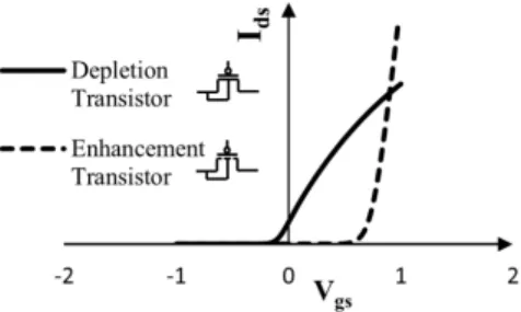
Fig. 3. Transfer characteristic of depletion- and enhancement-mode transistor
A. Depletion MOSFET characteristic
The depletion transistors are also called “normally-on” or “native” transistors. This mode is only available for N-type in most standard CMOS technologies. It uses only the low-level P-doped silicon substrate (native doping) instead of P-well doping to form the MOSFET channel. This MOS structure
forms a conductive channel beneath the gate oxide layer when the gate terminal voltage is at zero, then acts as a “normally-closed” switch. The gate source voltage must be negative to turn off the transistor. The transfer characteristic comparison between depletion- and enhancement-mode transistors in 0.18µm technology is shown in Figure 3.
The depletion transistor is widely-used in over-voltage protection, power supply startup and telecommunication applications. However, to the best of our knowledge, the depletion MOSFET has not been used in a harvesting circuit to decrease input voltage. In addition, only a few published works [7, 11] use this type of transistor in charge pumps but for higher voltage applications.
Fig. 4. TEG connection and 1:2 DCP
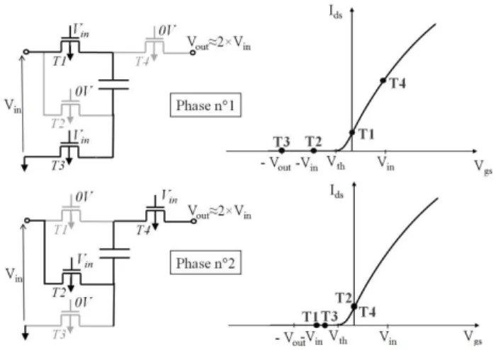
B. Proposed architecture: depletion-based charge pump
The proposed topology of a Depletion-based voltage doubler Charge Pump (DCP) is shown in Fig. 4. It is composed of four N-type depletion MOSFETs T1,2,3,4, a flying capacitance
Cfly and a ring oscillator (not shown here). As in Fig. 1, the
oscillator and gate drivers are still composed of enhancement MOSFETs supplied directly by the input voltage Vin. The
oscillator then works under the threshold voltage to generate the clock signal between 0 and Vin, and the gate drivers deliver
the same signal swing to the depletion MOSFET gates (Vg,i).
Fig. 5. Step-up capacitive switching converter in phase 1 and 2
In steady-state, Figure 5 shows the transistor states in both phases. The topology differs from Figure 1 because any transistors are not fully turn-off in both phases. In phase 1, transistors T1 and T3 are turned on whereas T2,4 are blocked.
This therefore creates the main conductive path from the input to charge the flying capacitor through T1,3. In phase 2, T2 is
conductive but T3 is still blocked and T4 is in on-state. The
flying capacitor discharges into Vout through T2 and T4. The
undesired conduction paths (e.g. T1,3 in phase 2) send charge in
the opposite direction making the circuit unable to boost the input to the ideal value (double the input here).
The issue with the proposed architecture is that the transistor cannot be fully turned off. Therefore, the main design consideration consists in distinguishing the different switch states to create a clear conductive path in both phases. Then, the optimal transistor sizing has to be found to balance the desired and undesired conductive paths. In the enhancement-based topology (Fig. 1), the on-state resistance is optimized in another way to balance the conduction and switching losses.
C. A good candidate for a “startup circuit”
The depletion transistor has a higher on-state resistance than the enhancement transistor for the same size, limiting the maximum achievable efficiency. Moreover, a not fully turned off behavior activates some undesired and inefficient conduction paths. Therefore, the proposed circuit is more suitable for a “startup circuit” than the “main harvesting circuit” which needs a higher achievable efficiency. After the startup phase without initial energy, the startup circuit provides enough energy to initialize the main circuit well. Then, a second harvester circuit using an ECP could be used to provide efficient conversion.
D. Topology refinement to reduce the startup time
The architecture presented in Fig. 4 could be improved by introducing two design refinements as shown in Fig. 6. The proposed High Swing Enhancement-based Charge Pump (HS-ECP) consisting of T1,2,3,4 is now driven by buffers and an
oscillator powered by Vout and Vneg. The Vneg signal is provided
by the inverter charge pump with 4 depletion transistors (T5,6,7,8). At the beginning, the tank capacitor is directly charged
by the input voltage through the normally-on transistors T1,4.
Then, the ring oscillator can start and provides a clock signal from Vneg to Vout. The key point is to boost the driving voltage
swing Vϕ1 and Vϕ2 by changing the power supply of the ring
oscillator. The full turn-off of the switches T1,2,3,4 avoids the
undesired conduction described in the previous section. Using the additional charge pump inverter, this topology produces a better power efficiency and reaches the 1:2 conversion ratio.
E. Higher conversion ratio using DCP approach
A higher conversion ratio can be achieved by adding extra charge pump stages to the proposed converter in Fig. 4. Figure 7 shows the 1:4 DCP.
Fig. 7. 1:4 depletion-based charge pump
IV. RESULTS
A. Comparison of ECP and DCP
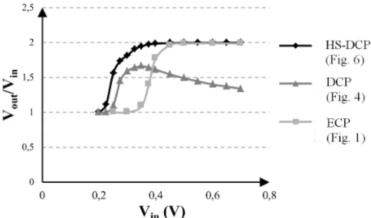
The proposed circuits (DCP and HS-DCP) and the basic architecture (ECP) were simulated and compared in terms of their start-up input voltage capability. The size of the ring oscillator is the same for the three topologies. The oscillation frequency is 12.8 kHz at 0.3V. The TEG has a 10Ω internal resistance and the value of the flying and tank capacitors are 1nF and 10nF, respectively. The comparison is made using the same overall gate surface i.e. . Figure 8 shows the conversion ratio regardless of the input voltage for the DCP, HS-DCP and ECP circuits in the doubler (Figs. 1, 4, 6).
Fig. 8. Conversion ratio v. input voltage for the three described topologies
Fig. 9. Conversion ratios in steady-state v. input voltage of the proposed architecture
As expected, the depletion modes allow lower input-voltage operation. With the HS-DCP, the output voltage is 150%
higher than the input voltage at 250mV compared to 400mV with the ECP. The HS-DCP doubles the input voltage above 400mV compared to 500mV with the ECP. Comparison of the DCP and HS-DCP indicates the need to power the ring oscillator between Vneg and Vout. It is especially true when the
input voltage is higher than 0.4V where the gate-source voltage is insufficient to turn on the transistor T4.
Figure 9 shows the performance of the HS-DCP for a higher conversion ratio. The startup circuit can provide conversion ratios greater than 2 (Figure 8) which allows voltages higher than 1V to be reached even with input voltages as low as 250mV for 1:8 topology.
B. Charging Time
Another advantage of the proposed circuit is to speed up the startup operation compared to the ECP. During the charging phase, the ECP transistors operate under their threshold voltage which leads to higher resistance and thus a longer charging time. In the DCP, the transistors always operate above their threshold voltage and allow more charge transfer at each period. Table 1 shows the startup time comparison in ms between both voltage doubler topologies (Fig. 1 and 3). As shown in Fig. 8, the ECP cannot reach the step-up operation when the input voltage is below 400mV leading to an infinite startup time.
TABLEI STARTUP TIME (MS) Vin Enhancement-based
Charge Pump (ECP)
Depletion-based Charge Pump (DCP) 0.25 18 0.30 5.5 0.35 3.7 0.40 126 1.6 0.45 23 1 0.50 3 0.7 0.60 0.04 0.5 C. Performance comparison
The key advantages of the charge pump using a depletion transistor compared to the state-of-the-art are:
• standard CMOS process compatibility,
• fully-integrated passive component,
• no post-fabrication processing needed,
• relative low start-up voltage (~250mV in this technology).
However, the main drawback of the proposed topology is the relatively low efficiency (around 50%). In fact, the depletion transistors are not fully turned off implying some leakage current. Therefore, this circuit is suitable as a startup function (cold start) but is insufficient for maximizing the power transfer from the harvester to the energy storage. The authors therefore suggest using a classical charge pump or inductive converter when the startup phase is finished.
V. CONCLUSION
To conclude, a low start-up voltage step-up DC-DC converter suitable for a battery-less harvester circuit is presented. The proposed charge pump topology is composed of a depletion transistor instead of an enhancement one to
allow sub-threshold operation. The solution improves the low voltage self-starting of the charge pump circuit. The transistor level simulation done in 0.18µ m CMOS technology shows a 250mV startup voltage using a depletion-based charge pump instead of 400mV in enhancement-based topology. The advantage compared to a state-of-the-art solution is to achieve a low voltage cold start for an energy harvesting circuit with standard CMOS technology without bulky external components or post-fabrication processing.
REFERENCES
[1] R.J.M. Vullers, et al., “Micropower energy harvesting”, Solid-State
Electronics, vol.53, pp 684-693, Apr. 2009
[2] I. Doms et al., “Integrated capacitive power-management circuit for thermal harvesters with output power 10 to 1000µW," IEEE
International Solid-State Circuits Conference - Digest of Technical Papers, , pp.300,301, 8-12 Feb. 2009
[3] J.P. Im et al. “A 40 mV Transformer-Reuse Self-Startup Boost Converter With MPPT Control for Thermoelectric Energy Harvesting”
IEEE Journal of Solid-state Circuits, vol.47, no. 12, pp. 3055-3067,
Dec. 2012
[4] Y.K. Ramadass, “A batterey-less thermoelectric energy harvesting interface circuit with 35mV startup voltage”, IEEE International
Solid-State Circuits Conference - Digest of Technical Papers, 2010
[5] J.U. Duncombe, “Infrared navigation-Part I: An assessment of feasibility,” IEEE Trans. Electron Devices, vol. ED-11, no. 1, pp. 34-39, Jan. 1959
[6] R. Vullers et al., “Micropower energy harvesting,” Solid-State
Electronics, n° 153, pp. 684-693, 2009
[7] A. Joita et al., “An active switch improved Dickson charge pump implemented in a BCD process,” Semiconductor Conference, vol. 2, pp. 437-440, 2012
[8] C. Huang and S. Chakrabartty, “Low-Threshold Voltage Mutlipliers based on Floating-gate Charge-pums,” IEEE Biomedical Circuits and
System Conference, pp. 205-208, 2008
[9] E. Mendez-Delgado and G.J. Serrano, “A 300mV start-up circuit for energy harvesting systems,” IEEE International Symposium on Circuits
and Systems, pp. 829-832, 2011
[10] M.B. Machado et al., “10mV-1V step-up converter fir Energy Harvesting Applications”, Proceedings of the 27th Symposium on
Integrated Circuits and Systems Design, no. 25, 2014
[11] M.W Oh et al., “Charge pump circuit for depletion-mode oxide TFTs,” Electronics letters, vol. 47, no. 6, pp. 378-380, 2011
[12] A. Montecuccp et al., “Simple, Fast and Accurate Maximum Power Point Tracking Converter for Thermoelectric Generators,” IEEE Energy Conversion Congress and Exposition (ECCE), pp. 2777-2783, 2012 [13] N. Degrenne et al., “Self-starting DC:DC boost converter for low-power
and low-voltage microbial electric generators,” IEEE Energy Conversion Congress and Exposition (ECCE), pp. 889-896, 2011 [14] J. Shin, “A New Charge Pump Without Degradation in Threshold
Voltage Due to Body Effet,” IEEE Journal of Solid State Circuit, vol. 35, no. 8, pp. 1227-1230, 2008
[15] B. Shen, “DC-DC converter Suitable for Thermoelectric Generator,” IEEE 24th International Conference on Thermoelectrics, pp. 529-531, 2005
[16] E. Carlson et al., “20mV input boost converter for thermoelectric energy harvesting,” Symposium on Very Large Scale Integration, pp. 162-163, 2009
[17] P.H. Chen, “0.18V input charge pump with forward body biaising in startup circuit using 65nm CMOS,” Custom Integrated Circuit Conference, pp. 1-4, 2010
[18] C. Veri et al., “A 40mV start up voltage DC-DC converter for thermoelectric energy harvesting applications,” IEEE Conference on PhD Research, pp. 1-4, 2014