HAL Id: hal-00877006
https://hal-iogs.archives-ouvertes.fr/hal-00877006
Submitted on 25 Oct 2013
HAL is a multi-disciplinary open access
archive for the deposit and dissemination of
sci-entific research documents, whether they are
pub-lished or not. The documents may come from
teaching and research institutions in France or
abroad, or from public or private research centers.
L’archive ouverte pluridisciplinaire HAL, est
destinée au dépôt et à la diffusion de documents
scientifiques de niveau recherche, publiés ou non,
émanant des établissements d’enseignement et de
recherche français ou étrangers, des laboratoires
publics ou privés.
Spontaneous emission enhancement at a photonic wire
miniband edge
Emilie Viasnoff-Schwoob, Claude Weisbuch, Henri Benisty, Ségolène Olivier,
Romuald Houdré, Christopher J. M. Smith
To cite this version:
Emilie Viasnoff-Schwoob, Claude Weisbuch, Henri Benisty, Ségolène Olivier, Romuald Houdré, et al..
Spontaneous emission enhancement at a photonic wire miniband edge. Optics Letters, Optical Society
of America - OSA Publishing, 2005, 30 (16), pp.2113-2115. �10.1364/OL.30.002113�. �hal-00877006�
Spontaneous emission enhancement at a
photonic wire miniband edge
E. Viasnoff-Schwoob*and C. Weisbuch
Laboratoire de Physique de la Matière Condensée Ecole Polytechnique, 91128 Palaiseau, France
H. Benisty
Laboratoire Charles Fabry de l’Institut d’Optique, Bat. 503, 91403 Orsay cedex, France
S. Olivier
Commissariat a l’Energie Atomique—Grenoble, Laboratoire d’Electronique de Technologie de l’Information—DOPT— Service Laboratoire Infrarouge, 17, Rue des Martyrs, 38054 Grenoble cedex, France
R. Houdre
Institut de Micro et Opto-electronique, Ecole Polytechnique Federale de Lausanne, CH-1015 Lausanne, Switzerland
C. J. M. Smith
Intense Photonics, 4 Stanley Boulevard, High Blantyre, G72 0UX, Scotland Received February 15, 2005
In a multimode photonic-crystal waveguide, we observe strong enhancement of the photoluminescence of embedded quantum dots at the edges of the so-called mini-stopband that were opened by Bragg diffraction between two guided modes. Taking into account light collection, we relate this observation to the singular photon density of states that is characteristic of a one-dimensional photon system. Furthermore, we quantify by how much the radiation losses smooth the divergence. For the first time to our knowledge, a clear account of the control of spontaneous emission in a one-dimensional system is thus demonstrated. © 2005 Optical Society of America
OCIS codes: 130.2790, 230.7370, 250.5300.
Periodic photonic structures exhibit interesting ef-fects, such as enhanced gain1–3 anomalous group ve-locity and dispersion,1,4 at the photonic-band edges. Notably, the control of the spontaneous emission of emitters inside these periodic structures has been widely investigated.5–9
One-dimensional (1D) photonic wires are of par-ticular interest, as evidenced by Kleppner10in 1981: A divergence of the photon density of states (DOS) oc-curs when the group velocity vanishes, either at mode cutoff frequency in typical wires or at band edge singularities in periodically structured wires.
Although 1D systems have been less investigated than their zero-dimensional counterparts,11 in-plane studies of such photonic crystal waveguides have al-ready shown the ability to lase at the band edge frequency.12 An out-of-plane experiment also exhib-ited an enhancement of the spontaneous emission power at such a band edge.13In this Letter we inves-tigate the change in the power spectrum of spontane-ous emission of quantum dots embedded inside a GaAs-based two-dimensional photonic crystal wave-guide at a mini-stopband edge singularity. Peaks on the side of this mode gap are observed in a pure spon-taneous emission regime; although they are reminis-cent of below-threshold side modes in common dis-tributed feedback laser diodes,14 no gain at all is involved here. Moreover, the excitation spot is very small, as it is diffraction limited. We relate these peaks to the calculated 1D photon density of states,
taking into account our collection geometry. This is what we believe is the first evidence of a photonic crystal based DOS divergence in a genuinely 1D sys-tem, with few discrete transverse modes.
The photonic crystal waveguides are carved in a triangular two-dimensional array of airholes defined by e-beam lithography and deep etching in a GaAs la-serlike heterostructure, fully similar to those re-ported earlier,15,16where a is the period of the trian-gular array, which contains three InAs quantum-dot
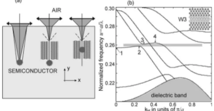
Fig. 1. (a) Internal light source and cleaved edge collec-tion: left to right, reference, measurement of waveguide transmission, measurement of emission from inside the photonic crystal waveguide. (b) Dispersion relation of the W3 waveguide (inset) with the mini-stopband of the funda-mental mode about the normalized frequency u = a / = 0.26 with ⑀ = 11.56 for the matrix and air filling factor f = 37%. 1–4, extrema of interest.
August 15, 2005 / Vol. 30, No. 16 / OPTICS LETTERS 2113
layers. Their in-plane photoluminescence is collected through the cleaved edge after propagation either in unpatterned areas or through a photonic crystal waveguide [Fig. 1(a)]. The waveguide [W3, Fig. 1(b)] is defined by three missing rows along the ⌫K direc-tion of the photonic crystal array. The specific band edges that we used here are on the band-structure diagram 共k兲 of Fig. 1(b) inside the photonic gap of the surrounding crystal. We work around the so-called mini-stopband of the W3 waveguide. This an-ticrossing is opened through Bragg diffraction be-tween the fundamental and 5th-order guided modes. Figure 1(a) shows the geometry used to probe the fundamental mode transmission in the W3 wave-guide. The raw spectrum is shown in Fig. 2, along with the smoothed source spectrum.17 The emission of quantum dots inside the waveguide is probed as follows: we excite the luminescence of quantum dots in the waveguide, at approximately 10m from its output. For the propagating waveguide modes we are thus in the opened-resonator regime.18 Figure 2 shows the raw spectrum collected on the cleaved edge, and Fig. 3(b) shows the ratio at the source spec-trum. A large peak and smaller peaks on the sides of the mini-stopband clearly appear. Their exact strength does not depend on excitation and collection conditions for a given setup, from a careful check. Op-tical amplification is ruled out by variable pumping data and from the diffraction-limited pumped area. The best peak-to-background ratio is in excess of 7. Similar peaks were observed for W3 waveguides of different lengths and for different excitation posi-tions along the waveguide as long as we stayed in the opened resonator regime for propagating modes.
We interpret these data as being due to the en-hanced 1D photon DOS of the photonic crystal wave-guide at the mini-stopband edges. This DOS is de-duced from the dispersion relation, including propagation losses. The losses of the different modes are precisely known from measurements.19,20 These values agree with the model whereby a fictitious imaginary dielectric constant in the airholes depicts propagation losses.21 The dispersion relation of Fig. 1(b) is calculated by use of a two-dimensional plane-wave expansion22 with the following parameters: ⑀GaAs= 11.56,⑀holes= 1 + 0.05i, and an air filling factor
of the photonic crystal array of f = 37%. A complex fre-quency is obtained: ˜ 共k兲 =
⬘
共k兲 + i⬙
共k兲, where ⬘
共k兲 is the standard dispersion relation of Fig. 1(b). Hav-ing such a physically correct value means that we can produce the proper smoothing of the 1D photon DOSsingularity at band edges, without any adjustable pa-rameter. With losses taken into account, the 1D DOS is simply the sum of Lorentzians, ⬃1 / 关−˜ 共k兲兴2 for
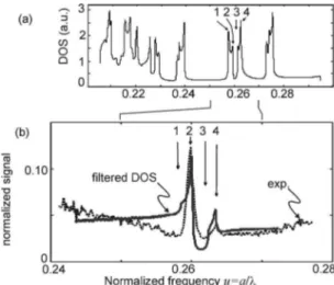
each k value of Fig. 1(b), with a fine enough k mesh [Fig. 3(a)]. It has four features, associated with ex-trema 1–4 of Fig. 1(b). This DOS is only the part of the photon DOS related to TE-polarized in-plane pho-ton states. To account for the experimentally ob-served results, we ignore the nonresonant mode con-tinuum of the slab claddings, as no light is collected there: our setup collects a small internal angle of ±7° about the normal, which contains chiefly guided modes of the photonic crystal waveguide.20 Nor is it required to specify a local DOS, as the quantum dots are excited across several waveguide unit cells (each 0.25m ⫻ 0.8m), overlapping ⬃90% of the horizon-tal mode profile.
What is needed, however, is to take propagation from the emission spot to the outside collected modes into account, an issue also met to some extent in pho-tonic crystal–opal related studies9(for opals with in-filtrated emitters, however, the local density of states is crucial, unlike here). Extrema 1 and 4 correspond to modes that have few chances of being detected: ex-tremum 4 involves two coupled modes with odd sym-metry, hence zero on-axis far field; extremum 1 in-volves a genuinely stationary mode, making unlikely a strong signal out of the lossy resonator.
The hybrid coupled modes about the mini-stopband suffer somewhat from being stationary as well, but, conversely, they also have a propagative component in the fundamental mode. We thus chose to modify the DOS by using a modal filter, mimicking the col-lection process as exactly as possible. A band-dependent coefficient C共k兲 weights the value of the DOS of each mode. We choose it as the relative weight in Fourier space of on-axis plane waves in the plane-wave spectrum of the in-plane mode’s magnetic field Hk共r兲= ⌺GhG共k兲exp关i共k + G兲r兴, that is, we privi-lege the presence of strong Fourier components for
Fig. 2. Raw spectra from the three configurations of Fig. 1(a). The reference has been multiplied by 0.15 and smoothed for clarity.
Fig. 3. (a) Calculated 1D DOS of the photonic wire with the data of Fig. 1(b) used for the real part of the dispersion relation and the imaginary part of the same dispersion when ⑀holes= 1 + 0.05i in the airholes. (b) Modified DOS, with the modal filter, superimposed by the experimental normalized spectrum of emission from the waveguide. 2114 OPTICS LETTERS / Vol. 30, No. 16 / August 15, 2005
plane waves that have zero transverse wave vector
G⬜= 0. G, the reciprocal wave vectors, and r, the po-sition vector, are two-dimensional, and 兵hG共k兲其 is the eigenvector obtained when one is computing the dis-persion relation of Fig. 1(b).22The important point is that singularity 2 of the in-plane DOS is preserved, while contributions of singularities 3 and 4, while they are measurable, cannot be clearly distinguished [Fig. 3(b)].
This modification convincingly establishes that the observed peaks arise from the 1D DOS singularities of the photonic-crystal-type wire.23 The W3 wave-guide provides a clear signature at well-defined spec-tral locations, with a large signal stemming from the proper area of the system. The role of the detection process is reduced to as simple physics as possible. Data from broader waveguides exhibit similar peaks at edges of their mini-stopbands.
In conclusion, the spontaneous emission singular-ity in the power spectrum expected in a one-dimensional photonic system has been evidenced by the photoluminescence of quantum dots in a GaAs-based photonic crystal waveguide. Full knowledge of the modes in a two-dimensional picture, and an ac-count of the collection process in a modal filter spirit, have provided a safe basis for this claim.
E. Viasnoff-Schwoob’s e-mail address is
hb@pmc.polytechnique.fr.
*Present address, Laboratoire de Photonique et Nanostructures, 91460 Marcoussis, France.
References
1. J. P. Dowling, M. Scalora, M. J. Bloemer, and C. M. Bowden, J. Appl. Phys. 75, 1896 (1994).
2. E. Schwoob, H. Benisty, C. Weisbuch, C. Cuisin, E. Derouin, O. Drisse, G.-H. Duan, L. Legouézigou, O. Legouézigou, and F. Pommereau, Opt. Express 12, 1569 (2004).
3. C. Monat, C. Seassal, X. Letartre, P. Regreny, P. Rojo-Romeo, P. Viktorovitch, M. Levassor d’Yerville, D. Cassagne, J.-P. Albert, E. Jalaguier, S. Pocas, and B. Aspar, Appl. Phys. Lett. 81, 5102 (2002).
4. D. Mori and T. Baba, Appl. Phys. Lett. 85, 1101 (2004).
5. M. D. Tocci, M. Scalora, M. J. Bloemer, J. P. Dowling, and C. M. Bowden, Phys. Rev. A 53, 2799 (1996). 6. M. Boroditsky, R. B. Vrijen, T. F. Krauss, R. Coccioli, R.
J. Bhat, and E. Yablonovitch, Proc. SPIE 3621, 190 (1999).
7. S. John and T. Quang, Phys. Rev. A 50, 1764 (1994). 8. S. T. Ho, in Optical Processes in Microcavities, R. K.
Chang and A. J. Campillo, eds. (World Scientific, 1996), p. 339.
9. P. Lodahl, A. F. van Driel, I. S. Nikolaev, A. Irman, K. Overgaag, D. Vanmaekelbergh, and W. L. Vos, Nature 430, 654 (2004).
10. D. Kleppner, Phys. Rev. Lett. 47, 233 (1981).
11. J. M. Gérard, B. Sermage, B. Gayral, B. Legrand, E. Costard, and V. Thierry-Mieg, Phys. Rev. Lett. 81, 1110 (1998).
12. A. Sugitatsu and S. Noda, Electron. Lett. 39, 213 (2003).
13. X. Letartre, C. Seassal, and C. Grillet, Appl. Phys. Lett. 79, 2312 (2001).
14. T. Makino and J. Glinski, IEEE J. Quantum Electron. 24, 1507 (1988).
15. H. Benisty, C. Weisbuch, D. Labilloy, M. Rattier, C. J. M. Smith, T. F. Krauss, R. M. De La Rue, R. Houdré, U. Oesterle, C. Jouanin, and D. Cassagne, J. Lightwave Technol. 17, 2063 (1999).
16. S. Olivier, C. J. M. Smith, M. Rattier, H. Benisty, C. Weisbuch, T. F. Krauss, R. Houdré, and U. Oesterle, Opt. Lett. 26, 1019 (2001).
17. D. Labilloy, H. Benisty, C. Weisbuch, C. J. M. Smith, T. F. Krauss, U. Oesterle, and R. Houdré, Phys. Rev. B 59, 1649 (1999).
18. C. H. Henry, J. Lightwave Technol. 4, 288 (1986). 19. S. Olivier, H. Benisty, C. Weisbuch, C. J. M. Smith, T.
F. Krauss, and R. Houdré, Opt. Express 11, 1490 (2003).
20. E. Schwoob, H. Benisty, C. Weisbuch, C. J. M. Smith, T. F. Krauss, R. Houdré, and U. Oesterle, J. Opt. Soc. Am. B 19, 2403 (2002).
21. H. Benisty, D. Labilloy, C. Weisbuch, C. J. M. Smith, T. F. Krauss, A. Béraud, D. Cassagne, and C. Jouanin, Appl. Phys. Lett. 76, 532 (2000).
22. H. Benisty, J. Appl. Phys. 79, 7483 (1996).
23. Assessment of the Purcell effect would, conversely, require knowledge of the full density of states, in plane and out of plane, a topic deferred to future research.