Publisher’s version / Version de l'éditeur:
Langmuir, 32, 34, pp. 8735-8742, 2016-08-10
READ THESE TERMS AND CONDITIONS CAREFULLY BEFORE USING THIS WEBSITE. https://nrc-publications.canada.ca/eng/copyright
Vous avez des questions? Nous pouvons vous aider. Pour communiquer directement avec un auteur, consultez la
première page de la revue dans laquelle son article a été publié afin de trouver ses coordonnées. Si vous n’arrivez pas à les repérer, communiquez avec nous à [email protected].
Questions? Contact the NRC Publications Archive team at
[email protected]. If you wish to email the authors directly, please see the first page of the publication for their contact information.
NRC Publications Archive
Archives des publications du CNRC
This publication could be one of several versions: author’s original, accepted manuscript or the publisher’s version. / La version de cette publication peut être l’une des suivantes : la version prépublication de l’auteur, la version acceptée du manuscrit ou la version de l’éditeur.
For the publisher’s version, please access the DOI link below./ Pour consulter la version de l’éditeur, utilisez le lien DOI ci-dessous.
https://doi.org/10.1021/acs.langmuir.6b02475
Access and use of this website and the material on it are subject to the Terms and Conditions set forth at
Analysis method for quantifying the morphology of nanotube networks
Vobornik, Dusan; Zou, Shan; Lopinski, Gregory P.
https://publications-cnrc.canada.ca/fra/droits
L’accès à ce site Web et l’utilisation de son contenu sont assujettis aux conditions présentées dans le site LISEZ CES CONDITIONS ATTENTIVEMENT AVANT D’UTILISER CE SITE WEB.
NRC Publications Record / Notice d'Archives des publications de CNRC:
https://nrc-publications.canada.ca/eng/view/object/?id=2aa69af3-2e4c-4587-90a4-b412e0dee323 https://publications-cnrc.canada.ca/fra/voir/objet/?id=2aa69af3-2e4c-4587-90a4-b412e0dee323
1
Analysis Method for Quantifying the Morphology of Nanotube
2
Networks
3
Dusan Vobornik,
*
Shan Zou, and Gregory P. Lopinski
4Measurement Science and Standards, National Research Council Canada, 100 Sussex Drive, Ottawa, Ontario K1A 0R6, Canada 5
*
S Supporting Information6 ABSTRACT: While atomic force microscopy (AFM) is a powerful
7 technique for imaging assemblies and networks of nanoscale materials, 8 approaches for quantitative assessment of the morphology of these 9 materials are lacking. Here we present a volume-based approach for 10 analyzing AFM images of assemblies of nano-objects that enables the 11 extraction of relevant parameters describing their morphology. Random 12 networks of single-walled carbon nanotubes (SWCNTs) deposited via 13 solution-phase processing are used as an example to develop the method 14 and demonstrate its utility. AFM imaging shows that the morphology of
15 these networks depends on details of processing and is influenced by choice of substrate, substrate cleaning method, and 16 postdeposition rinsing protocols. A method is outlined to analyze these images and extract relevant parameters describing the 17 network morphology such as the density of SWCNTs and the degree to which tubes are bundled. Because this volume-based 18 approach depends on accurate measurements of the height of individual tubes and their networks, a procedure for obtaining 19 reliable height measurements is also discussed. Obtaining quantitative parameters that describe the network morphology allows 20 going beyond qualitative descriptions of images and will facilitate optimizing network preparation methods based on measurable 21 criteria and correlating performance with morphology.
22
■
INTRODUCTION23Nano-objects such as nanotubes, nanowires, nanosheets, and 24nanoparticles continue to be of interest as building blocks for 25functional materials due to their remarkable size-dependent 26properties. However, the properties of materials constructed 27from these objects depend not only on the properties of the 28objects themselves but also on how these blocks assemble into 29larger structures.1−3 Although electron and scanned probe 30microscopies are commonly used to visualize the morphology 31of these assemblies, methods for quantitative assessment of the 32resulting images have received less attention. Extraction of 33quantitative parameters describing the morphology of a sample 34from images will facilitate feedback on how processing affects 35the structure and ultimately how the structure influences the 36properties of the material.
37 While the analysis approach presented here should be widely 38applicable to a range of nanoscale materials, random networks 39of single-walled carbon nanotubes deposited from solution are 40used as an example to illustrate the method and demonstrate its 41utility. These networks represent interesting model systems for 42investigating the interplay between the intrinsic properties of 43the individual nanoscale building blocks and process-dependent 44network morphologies in determining properties. While 45individual single-walled carbon nanotubes (SWCNTs) exhibit 46high intrinsic conductivities and field effect mobilities, films 47based on random networks of these tubes show considerably 48lower values.1,4−7Over distances greater than the length of an 49individual tube, electrical transport is usually limited by tube− 50tube junctions, making the conductivity highly dependent on
51
details of the network morphology (i.e., tube density, bundling,
52
and alignment).8−12 Furthermore, starting with the same 53
carbon nanotube ink, process details can strongly influence
54
the morphology and consequently the electronic properties of
55
the network.13
56
Atomic force microscopy (AFM) is a powerful and versatile
57
probe of nanomaterial morphologies, enabling imaging of the
58
individual nano-objects and their assemblies in a variety of
59
environments (vacuum, ambient, liquid) and regardless of
60
whether these materials are insulating or conducting.
61
Quantitative AFM studies of nanomaterials have typically
62
focused on extracting distributions of lengths, heights, or
63
diameters for individual nano-objects.14−19Obtaining this type 64
of data usually requires optimizing sample preparation
65
conditions so that isolated features can be imaged on a flat
66
substrate. However, functional assemblies are most often
67
achieved at higher densities. For example, the formation of
68
conductive networks of nanowires and nanotubes for
69
applications such as transparent conductive electrodes or
70
channel materials for thin film transistors (TFTs) requires
71
densities above the percolation threshold. At these higher
72
densities there is likely to be some degree of overlap and
73
aggregation of the individual building blocks. In these realistic
74
applications it is often hard to see where one nano-object ends
75
and the other starts, making it difficult to accurately count the
Received: July 4, 2016 Revised: August 5, 2016
Article
pubs.acs.org/Langmuir
Published XXXX by the American Chemical
Society A DOI:10.1021/acs.langmuir.6b02475
76exact number of objects in the network. Among several 77measurands that can be used to characterize the morphology of 78a random network of nanowires or tubes, two that are 79particularly important in determining electronic and optical 80properties are the tube density and the extent to which the 81individual tubes aggregate into bundles. In this work a 82straightforward and fast volume-based method to extract 83these measurands from experimentally obtained AFM images 84is presented. The use of a volume-based analysis method means 85that the accuracy of AFM height measurements (from which 86the volume is calculated) is of paramount importance. 87Therefore, we also propose an experimental procedure that 88facilitates verification of the AFM imaging parameters to ensure 89reliable measurements of the nanotube height.
90
■
EXPERIMENTAL SECTION91 Substrate Preparation. Two different substrates were used; a 92thermally grown SiO2thin film on silicon, and highly ordered pyrolytic
93graphite (HOPG). A silicon wafer with a 100 nm thick thermal oxide 94(Silicon Quest International) was cut into 1 cm2 pieces. Prior to
95nanotube network deposition the silicon oxide surface was cleaned by 96either: (a) Piranha solution bath (3:1 volume ratio of 98% H2SO4and
9730% H2O2) for 30 min, followed by thorough rinsing with ultrapure
98water (resistivity of 18.2 MΩ·cm), and blown dry with nitrogen; or (b) 995 min in an oxygen plasma cleaner (Yield Engineering Systems G-100500). For the HOPG substrates, we used ZYB-grade, 12 mm × 12 mm 101HOPG squares (Bruker AFM Probes, Camarillo, CA). Clean surfaces 102were obtained by cleaving off the top layers with Scotch tape prior to 103nanotube network deposition.
104 SWCNT Network Preparation. A commercially available ultra-105high purity semiconducting SWCNT dispersion was purchased from 106Nanointegris (http://www.nanointegris.com/IsoSol-S100). The sepa-107ration and purity of these nanotubes are ensured by the poly(9,9-di-n-108dodecylfluorene) (PFDD) wrapping.20 Networks were prepared by 109dropcasting 40 μL of a 10 mg/L toluene solution of the nanotubes on 110clean substrates and letting the toluene evaporate. This typically took 11110 to 15 min. To remove excess polymer (initial polymer to nanotube 112mass ratio was 4 to 1), as well as any other contaminants, we rinsed 113the samples upon solvent evaporation with a steady stream of toluene 114for 20 s or by successive 20 s rinses of toluene, tetrahydrofuran (THF), 115and isopropanol (IPA). Finally, samples were dried with nitrogen and 116stored in a closed Petri dish under room conditions. AFM 117measurements were carried within a day of preparation, but several 118samples were again measured at different times during several months 119following their preparation with no significant changes in morphology 120observed.
121 Chemicals. Toluene and tetrahydrofuran were purchased from 122EMD Millipore with respective purities (GC) of ≥99.5 and ≥99.9%. 123Distilled in glass-grade isopropanol was purchased from Caledon 124Chemicals with a purity (GC) of ≥99.7%.
125 AFM Imaging. The samples were imaged using the MultiMode 126AFM with the NanoScope V controller (Bruker Nano Surfaces 127Division, Santa Barbara, CA) in Bruker’s proprietary PeakForce QNM 128mode. The peak force with which the tip taps the sample surface was 129always kept close to the lowest stable imaging level of 0.5 nN or less 130(stable here means perfectly overlapped trace and retrace lines during 131AFM scanning). We have used ScanAsyst-Air AFM probes (Bruker 132AFM Probes, Camarillo, CA), which are made of silicon nitride and 133whose typical tip radius is 2 nm according to the manufacturer’s 134specifications.
135 Analysis Software. All analysis of AFM images was performed 136using Gwyddion, a free, open-source software, with well-defined and 137explained operations and functions.21
138
■
RESULTS AND DISCUSSION139 Process Details Influence SWCNT Network Morphol-f1 140ogy. AFM images of SWCNT networks processed in slightly
141 f1
different ways are shown in Figure 1. The rather different
142
morphologies readily apparent in these images illustrate how
143
details of sample processing influence network formation, even
144
starting from the same SWCNT dispersion. Specifically, the
145
observed network variations result from the use of different
146
substrates, different substrate cleaning procedures, or different
147
postdeposition rinsing procedures, as detailed in the figure
148
caption. It is easy to qualitatively observe certain differences
149
between the networks inFigure 1. For example, there seems to
150
be more tubes on the oxygen plasma-cleaned (Figure 1c) versus
151
piranha-cleaned SiO2surface (Figure 1a). Similarly, it appears 152
that additional rinsing with tetrahydrofuran and isopropanol
153
(Figure 1b) leads to more features greater than 5 nm in height,
154
indicative of substantial aggregation (bundling) of the
155
SWCNTs, yet putting numbers on these differences appears
156
to be very difficult.
157
Some representative cross sections from Figure 1a
158
(numbered white lines) are shown in Figure 1e. While the
159
SWCNTs used to make the dispersions used here have a
Figure 1.AFM images of networks obtained by dropcasting the same solution of carbon nanotubes on SiO2(a−c) and HOPG (d). Prior to
deposition, SiO2 substrates were cleaned either by Piranha solution
(a,b) or by oxygen plasma treatment (c), while HOPG was freshly cleaved (d). Upon solvent evaporation samples were rinsed with toluene for 20 s (a,c,d) or sequentially with toluene, tetrahydrofuran, and isopropanol for 20 s each (b). All images have the same 1 μm2size
and are displayed with the same 9 nm vertical scale, where 0 corresponds to the lowest pixel height in the image. Cross sections in panel e correspond to numbered lines shown in panel a.
Langmuir Article
DOI:10.1021/acs.langmuir.6b02475
LangmuirXXXX, XXX, XXX−XXX
160narrow distribution of diameters ranging from 1.2 to 1.4 nm, 161simple geometric analysis shows that if there was no polymer 162wrapped and we took the three smallest 1.2 nm diameter 163nanotubes and bundled them together into a tight pack as 164illustrated in the Supporting Information Figure S1 (i), the 165bundle height would still not exceed 2.24 nm. On the basis of 166this, network features whose height is above 2 nm are 167considered to be bundles consisting of several nanotubes with 168some degree of vertical stacking, while features whose height is 169<2 nm are assumed to be individual SWCNTs (also see part 1 170ofSupporting Information). With this assumption, the analysis 171of cross sections in our AFM images indicates that the presence 172of the PFDD polymer increases the average single nanotube 173diameter to 1.7 nm, with the height distribution of isolated 174nanotubes ranging from 1.4 to 2 nm (data not shown, based on 175the analysis of the AFM measured height of 120 individual 176nanotubes rinsed with toluene). To illustrate this, profiles 2, 4, 177and 6 inFigure 1e, whose height is close to 1.7 nm, correspond 178to single or laterally aligned nanotubes and not to bundles. On 179the contrary, profiles 1, 3, 5, and 7, with heights clearly 180exceeding 2 nm, are considered to be bundles. This simple 181analysis indicates that for these networks many of the features 182seen in the AFM images are in fact bundles of more than one 183tube, and simple counting of features will underestimate the 184tube density. The remainder of this article focuses on 185developing a method that allows quantifying the morphology 186of these networks by extracting meaningful parameters from
187
these images. These parameters can then be used to compare
188
different network fabrication process and correlate resulting
189
morphologies with properties of the networks.
190
Volumetric AFM Analysis for Carbon Nanotube
191
Networks. Volumetric analysis of AFM data has been
192
proposed in the past, but it was based on an apparent mass−
193
volume relationship15and did not offer adequate solutions for
194
high surface density, partly overlapping, or bundled samples. In
195
this work, we present a volumetric analysis method that does
196
not rely on any mass−volume equivalency and which works
197
well even for dense and highly bundled samples. Using carbon
198
nanotube networks, we show how this volume-based analysis
199
can quantify the degree of bundling and offer a straightforward
200
analysis method for a dense network, where it is often
201
impossible to make out individual nanotubes. As discussed
202
above (and also highlighted in the part 1 of the Supporting 203 Information), a particular challenge when trying to quantify
204
nanotube assemblies is the tendency for individual tubes to
205
bundle. Even with the use of polymers to disperse the
206
nanotubes, most of the SWCNTs in a realistic network are
207
observed to be bundled.
208
The method proposed here is based on a simple hypothesis
209
that the volume of a bundle of nanotubes is equal to the
210
product of the volume of a single nanotube by the number of
211
nanotubes in the bundle = ×
V N V
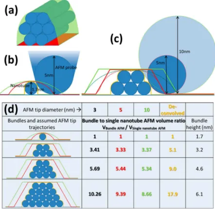
bundle of N nanotubes single nanotube (1) 212 Figure 2.(a) Scheme showing a bundle of seven nanotubes. The bundle’s projected AFM surface is shown in red, and together with the green surface on the top it illustrates the boundaries within which the volume of the bundle is calculated. (b) Cross section showing a 1.7 nm diameter nanotube being scanned by a 5 nm diameter AFM probe. The red line corresponds to the trajectory of the lowest point of the tip during scanning. The green line shows a similar trajectory that would result from a 10 nm diameter AFM tip scanning the same nanotube, and the orange line shows the ideally deconvoluted trajectory. (c) Trajectories for the 5 and 10 nm diameter AFM tips are shown in dashed red and green lines, the ideal deconvoluted contour is shown in orange, and the trapezoid shaped approximated contours that we used in calculations carried out in panel d are shown in solid red and green lines. (d) Table based on dividing the calculated AFM volume of a bundle by the calculated AFM volume of a single nanotube for three different AFM tip diameters as well as for deconvoluted AFM images. The table highlights the error of the volume based analysis if the deconvolution is not applied.
DOI:10.1021/acs.langmuir.6b02475
LangmuirXXXX, XXX, XXX−XXX
213Calculations to assess the validity of this hypothesis are f2 214summarized in Figure 2.
215 Practically, we propose to use AFM images to measure the 216volume of the entire network in an AFM image and then to 217divide it by the volume of a single, average nanotube, thus 218determining the number of equivalent SWCNTs in the image. 219Upon analyzing lengths and diameters of 30 single nanotubes 220(with height <2 nm and for which we could unambiguously 221distinguish both ends), the average nanotube length was 222determined to be 700 nm and the average diameter was 1.7 nm. 223The representative nanotube with dimensions close to these f3 224average values is shown inFigure 3e, and it was this nanotube 225that was used to obtain the single nanotube volume and 226projected surface used in the analysis later on. Upon 227determining the number of nanotubes in an image, the density 228can be easily expressed as this number divided by the total 229image surface.
230 In general, it is difficult to determine the exact number of 231tubes in a bundle. We propose a simple approach to quantify 232the degree of vertical bundling that uses the fact that upon 233bundling the volume of the bundle increases at a significantly 234higher rate than the projected surface of the bundle.Figure 2a 235shows a cartoon depicting a bundle of seven nanotubes, and the 236red surface underneath indicates schematically how its 237projected surface would look in the AFM image. The projected 238surface of this seven nanotube bundle is actually barely bigger 239than the projected surface of just three aligned nanotubes, yet 240its volume is much larger. Using this, one can define a 241parameter CBthat we will call the bundling coefficient
= − × C S S 1 V V B Net 1CNT Net 1CNT 242 (2)
243 In eq 2, SNet is the projected network surface, VNet is its 244volume, V1CNT is the volume of the average single nanotube, 245and S1CNT is its projected surface. The bundling coefficient
246
defined by the eq 2 is a number between 0 and 1, where 0
247
means that there is no bundling (moreover, for CB= 0 all of the 248
nanotubes would have to lie on the surface without even
249
crossing over each other), and 1 is the limit value that would be
250
approached if all the nanotubes were stacked one on top of
251
each other in a single vertical bundle. This coefficient is not the
252
exact fraction of bundled nanotubes but rather an indication of
253
the degree of vertical bundling where low CBvalues (closer to 254
0) indicate low rates of bundling and high CBvalues (closer to 255
1) indicate significant bundling. The comparison of CBfor two 256
samples prepared using different protocols would clearly
257
demonstrate which protocol leads to more or less bundling.
258
Deconvolution to Minimize the AFM Tip Size Effects.
259
In Figure 2a, the volume of a bundle, as measured using the
260
AFM, is shown as the volume enclosed by the green surface
261
from above (larger than the actual nanotubes volume due to the
262
AFM tip shape and the resulting tip-size-dependent
con-263
volution) and the red surface underneath. In general, the size of
264
a feature in an AFM image is always affected by the convolution
265
resulting from the shape of the tip. This is illustrated inFigure 266 2b, where the trajectory of the lowest point of a 5 nm diameter
267
AFM tip is shown in red when scanning a 1.7 nm diameter
268
nanotube. This trajectory represents an ideal AFM image,
269
where the tip gets in contact with the sample without
270
compressing or modifying it in any way. The scheme inFigure 271 2b shows that, even with this relatively sharp tip, the
272
convolution effect is significant, essentially tripling the volume
273
of a single nanotube. With a larger 10 nm diameter tip (green
274
trajectory) the resulting convolution error becomes even more
275
significant. A general rule is that the tip convolution becomes
276
more substantial with increasing tip size and decreasing tube
277
diameter. Because the sharpest commercially available AFM
278
tips are in the 2 to 4 nm radius range and the average diameter
279
of our nanotubes is 1.7 nm, the tip-related convolution will
280
likely be significant in AFM images. Furthermore, the
281
convolution effect is not equally affecting single nanotubes
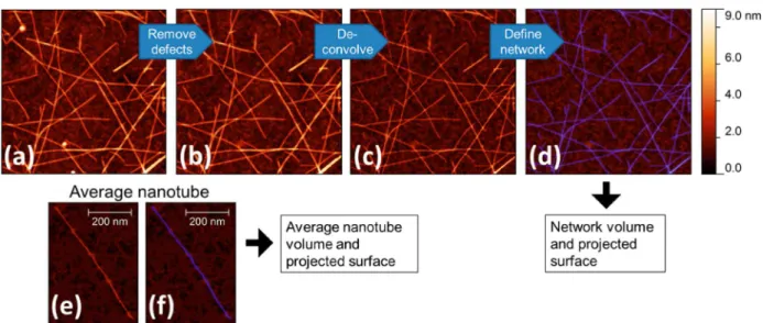
Figure 3.Analysis method outline based on the Gwyddion SPM analysis software: (a) Flattened image of a nanotube network. (b) Network defects such as non-nanotube contaminants were removed using “Small defect interpolation”. (c) A tip-deconvoluted image was obtained using “Surface reconstruction” function and an estimate of the tip diameter based on the value of the tip−substrate van der Waals interaction. (d) Network is defined by setting a height threshold to define a mask (in blue) such that both the amount of blue bleeding onto the substrate and the amount of network that is not colored blue are minimized. To complete the analysis, we analyzed a single average nanotube in the same way ((e) deconvoluted and flattened and (f) masked average nanotube), and its volume and projected surface are used to normalize the network data to extract the equivalent nanotube surface density and the degree of bundling. All images are displayed at the same 9 nm vertical scale and have a pixel density of 512 × 512 pixels par μm2. Panels a−d show 1 μm2of the network’s surface.
Langmuir Article
DOI:10.1021/acs.langmuir.6b02475
LangmuirXXXX, XXX, XXX−XXX
282and nanotube bundles of different sizes. In Figure 2the table 283(panel d) shows an estimate of the convolution effect as a 284function of both the tip size (calculations for 3, 5, and 10 nm 285tip diameters) and the bundle size (1, 5, 9, and 18 nanotube 286bundles). The data in the table (panel d) are obtained by 287calculating volumes of a single nanotube as imaged with varying 288size tips (the calculation is based on the assumption that the tip 289is in contact with the sample and that no deformations occur 290during imaging) and then calculating volumes of the bundles 291imaged with the same tips. For each tip size, the calculated 292bundle volume was divided by the calculated single nanotube 293volume, and the resulting number is shown in an appropriate 294tip-size column (color coded, black for the 3 nm tip, red for the 2955 nm tip, and green for the 10 nm tip). The results show that 296convolution with an AFM tip of a realistic size always leads to 297an underestimation of the number of nanotubes in a bundle 298when performing the volumetric analysis. For example, when 299the AFM measured volume of a bundle composed of five 300nanotubes is divided by the AFM measured volume of a single 301nanotube, both being imaged using a 10 nm diameter tip, the 302result is 3.37, when it should be 5. Calculations show that, as 303expected, smaller tips lead to slightly less error in the volume-304based estimation, whereas the error is greater for larger bundles. 305For example, for an 18 tube bundle measured with a 10 nm tip 306the error is more than 50% (8.66 instead of 18). The result was 307somewhat surprising, as one could expect to see the opposite 308trend due to all of the volume between the nanotubes in the 309bundles, leading to an overestimation of the number of 310nanotubes. However, the results demonstrate that the over-311estimation of the volume of the single nanotube due to the 312convolution by the tip size has a much larger effect.
313 For the AFM−volume calculations in Figure 2, tip 314trajectories were always based on the assumption that the tip 315gets in contact with nanotubes and the substrate without 316deforming them. The length of the single nanotube and that of 317bundles are assumed to have equal values. The diameter of each 318of the nanotubes was set to 1.7 nm, and the nanotubes in 319bundles were assumed to be confluent and packed as tightly as 320possible, as shown in the cartoons. To simplify calculations, we 321approximated the tip trajectory on top of bundles to isosceles 322trapezoid-like trajectories, where the base of the trapezoid 323corresponds to the point where the tip (its side) first gets in 324contact with the bundle, and the angle that the trapezoid side 325forms with its base is 60°, as shown inFigures 2c,d.Figure 2c 326also shows the exact trajectories for 5 and 10 nm diameter tips 327with dashed lines, and one can see that the trapezoid 328approximation leads to a somewhat bigger bundle volume, 329which should lead to a larger estimated number of nanotubes, 330and yet the convolution effect is sufficiently significant to make 331this approximation error irrelevant: The actual estimated 332numbers of nanotubes with the trapezoid approximation are 333still much smaller than the actual numbers of nanotubes 334forming the bundles.
335 The orange trajectory inFigure 2c corresponds to an ideally 336deconvoluted trajectory. While typical deconvolution algo-337rithms may not reach this degree of surface reconstruction, they 338still lead to a significant improvement in the quantitative 339volume estimation. We have used the Gwyddion SPM analysis 340software deconvolution erosion algorithm, which is well 341described,14 and appears to perform well (all of the 342deconvoluted images corresponding to raw images in Figure 3431are shown in theSupporting Informationpart 3). The orange 344column in Figure 2d shows that deconvolution leads to
345
recovering very accurate data based on volumetric analysis. An
346
example of how the deconvolution software affects the image is
347
also shown inFigure 3, where panel b shows a network image
348
prior to and panel c shows it after the deconvolution. In all of
349
the examples shown here the deconvolution was performed
350
using the “surface reconstruction” function in Gwyddion (Data
351
Process → Tip → Surface Reconstruction). This is an erosion
352
algorithm based on a probe−sample interaction modeling that
353
uses a purely geometrical approach. The choice of the tip
354
model is essential for the deconvolution, where both the shape
355
and the size of the tip have the most significant impact on the
356
final deconvoluted image. In-depth discussion on how the most
357
realistic tip size was determined is presented in theSupporting 358 Informationpart 2. The exact settings that we have chosen to
359
model the tip were a “pyramid” tip with 24 sides with an angle
360
of 20° and the radius that was determined using the van der
361
Waals force-based tip radius estimation described in part 2 of
362
theSupporting Informationand here below.
363
A certain amount of statistics is necessary and several areas
364
have to be imaged to take into account regional sample
365
heterogeneity to get quantitative and reliable data on nanotube
366
networks. If different preparation methods are compared, the
367
same procedure has to be done for each different network, and
368
it is likely that several AFM probes will be used in the process
369
or that the probe used is going to undergo some amount of
370
degradation, which typically translates into larger tip size as the
371
imaging progresses. To have a reliable comparison of data
372
acquired with different probes, or with the same probe that
373
gradually degrades with time, it is important to deconvolute the
374
images using the size of the tip when imaging was done.
375
There are several ways to determine the tip radius at the time
376
of the image acquisition: (1) imaging of an appropriate test
377
sample before and after the network imaging; (2) imaging of
378
well-characterized fiducial marker that would have to be
379
deposited together with the sample of interest; (3) blind tip
380
estimation, where the analysis software uses the actual network
381
image to try determining the tip’s shape and size; and (4)
382
recording and using van der Waals tip−sample interactions to
383
calculate the tip size.
384
While each of the above tip-size determination methods has
385
its own drawbacks and advantages, we have opted to use the
386
van der Waals based method, which may not be the most
387
precise one but is timely and minimally invasive, and therefore
388
the most practical one in our view. The calculation assumes that
389
the tip has a spherical shape and uses the fact that the van der
390
Waals force between a spherical tip and a planar substrate is
391
directly proportional to the tip diameter (see details in the
392 Supporting Informationpart 2).
393
Application of Analysis Procedure. Gwyddion SPM
394
analysis software offers a straightforward way of calculating the
395
network volume as well as the volume of an average nanotube,
396
and we have broken the optimal procedure to do this into the
397
simple steps shown in the Figure 3.Figure 3a shows an AFM
398
image that has been flattened using a polynomial fitting of the
399
substrate. To have only the volume and projected surface of the
400
network, without including eventual “contaminants” (e.g.,
401
unbound polymer, catalyst particles, amorphous carbon, or
402
other random contaminants), we eliminated any non-nanotube
403
like features from the image prior to further analysis. Our
404
samples appear relatively clean in general, and the contaminants
405
that we are talking about are usually a couple of small roundish
406
features similar to those that can be seen inFigure 3a. There is
407
a variety of ways to do this, but we found that Gwyddion’s DOI:10.1021/acs.langmuir.6b02475
LangmuirXXXX, XXX, XXX−XXX
408“remove spots” tool, which uses the “hyperbolic flatten”
409function to interpolate selected parts of the image, is 410particularly effective. Figure 3b shows the result of such a 411removal of several small contaminants that were present in 412panel a. Figure 3c shows the deconvoluted image. Finally, we 413have selected a height threshold that instructs the software that 414any part of the image that is higher than that value is a part of 415the network, and anything lower is the substrate. This is done 416by using Gwyddion’s “mark grains by threshold” function, and 417the resulting network is shown in blue (Figure 3d). If the 418threshold is chosen too low, much of the substrate will appear 419in blue, too, particularly for rough substrates. The flatter the 420substrate, the more accurate the threshold choice becomes. If 421too high a threshold value is chosen, parts of the nanotubes that 422form the network, or the nanotube edges, will not be blue and 423will therefore not be included in the calculation of the volume. 424The threshold selection part of the analysis is a critical part for 425getting a reliable and reproducible volumetric analysis. This is 426the biggest contributor to the uncertainties associated with the 427parameters extracted using our volumetric analysis method. 428 Once the network versus substrate parts of the image are 429defined, it is straightforward to get the total network volume 430and its projected surface by clicking on “Distributions of grain 431characteristics” button in the Gwyddion main menu. We chose 432to have the volume calculated using “Laplacian background 433basis”, where Gwyddion interpolates eventual surrounding 434substrate topography variations from the network volume to 435get more accurate results. The part of the analysis relying on 436the Gwyddion software is explained in detail in a software-437supporting publication.14
438 To complete the analysis, we performed the same cleanup/ 439deconvolution/network-definition procedure on an individual 440average nanotube, and Figure 3e,f show the average nanotube 441before and at the end of analysis, respectively. As a reminder, 442the average nanotube here was selected by analyzing lengths 443and cross sections of 30 individual tubes in networks of the 444same solution dispersed on silicon oxide and rinsed with 445toluene. This resulted in the average length and diameter of, 446respectively, 700 and 1.7 nm. Finally, the volume of the 447network is divided by the volume of the single nanotube to 448obtain the number of equivalent tubes contained in the 449network. This value is then divided by the entire surface of the 450image of the network, resulting in the network density. Then, 451eq 2is used to calculate the bundling coefficient.
452 Using the volumetric analysis outlined in detail above, the 453SWCNT density and bundling coefficient are calculated for the 454four different networks shown in Figure 1, with the results t1 455summarized inTable 1. The quantitative results confirm some 456of the qualitative observations discussed above. For example, 457comparing the networks on Piranha- and plasma-cleaned silicon 458dioxide, the SWCNT density is almost twice as large in the 459latter. Perhaps less obviously, the SWCNT density for the 460networks in Figure 1a,b are quite similar, with the main 461difference between these networks being a large increase in the 462bundling coefficient associated with the additional rinsing steps. 463The ability to quantify these morphology differences by the
464
approach outlined above will enable the correlation of process
465
details with resulting network structures and ultimately with the
466
properties of the nanomaterial. Although some of the results
467
reported here could be obtained on less dense networks by
468
patient drawing of cross sections and counting of individual
469
tubes, the method proposed here offers a more general and
470
time effective means to extract these parameters.
471
AFM Height Reliability Test. An aspect of AFM imaging
472
that has drawn scrutiny is the reliability of the height data.22,23
473
The height of nanoscale objects measured by AFM is often
474
smaller than the true value. There are several reasons that can
475
lead to this height underestimation, the most commonly
476
evoked one being that the AFM probe compresses the sample
477
during scanning. If the measured heights underestimate the real
478
height, this would negatively impact the reliability of the
479
volume based analysis proposed here. To verify the reliability of
480
the AFM height measurements, we used a simple test involving
481
successive imaging of the same network area using increasing
482 f4
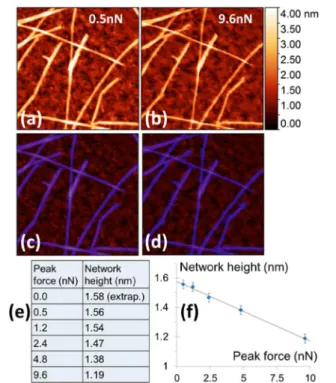
peak force set points.Figure 4shows the results from one such
483
test where the same network area was scanned five times,
484
starting at a peak force set point of 0.5 nN (image shown in Table 1. Results of the Volumetric Analysis of AFM Images of SWCNT Networks Prepared by Different Methods and Shown in
Figure 1
Piranha, toluene Piranha, tol+THF+IPA plasma, toluene HOPG, toluene
nanotubes per μm2 37 ± 8 44 ± 4 70 ± 14 52 ± 8
bundling coefficient 0.29 ± 0.03 0.61 ± 0.02 0.41 ± 0.01 0.49 ± 0.03
Figure 4.AFM height depends on the peak force applied by the tip during imaging: (a,b) Representative 300 × 300 nm2images of the
same area of a nanotube network acquired with a different peak force of (a) 0.5 and (b) 9.6 nN. (c,d) The same AFM images that are shown in panels a and b but we show in blue all of the network pixels that were used to calculate the average network height. That height is shown as a function of force in panels e and f for a range of five different peak force feedback values. In panel f the height data was fitted with a straight line, and the line value at 0 force is used to extrapolate the average network height shown in the first line of the table (e).
Langmuir Article
DOI:10.1021/acs.langmuir.6b02475
LangmuirXXXX, XXX, XXX−XXX
485Figure 4a) and ending with a peak force set point of 9.6 nN 486(Figure 4b). Careful comparison of the two images (displayed 487with the same vertical scale) indicates that the nanotubes 488appear slightly lower at the higher set point.
489 To analyze these images a height threshold value was chosen, 490as discussed above, to separate the network from the substrate. 491The result of defining this mask is shown in blue inFigure 4c,d. 492The average network height was then calculated as the average 493of the heights of all pixels in the masked area minus the average 494height of all the unmasked pixels (the substrate). The 495uncertainty on the height threshold results in the error bars 496shown in Figure 4f. Similar data were acquired a dozen times 497on different areas and on different samples with the same trend 498being observed, although absolute values vary to some extent. 499The measured height exhibits a linear decrease as the force 500increases. Fitting the height versus compression force curve 501with a straight line enables extrapolation of the measured height 502in the absence of applied force, as shown in theFigure 4f. 503 For all images shown inFigure 1, we used the same peak 504force feedback value of 0.5 nN. The average network height at 505this force feedback as extracted from the image inFigure 4a is 5061.56 nm. This is lower than the average individual nanotube 507diameter because this value takes into account all of the blue 508pixels and not just the ones that are on top of nanotubes that 509matter in the diameter calculation. (The height of pixels on 510sides of nanotubes and close to the substrate is taken into 511account in this average network height calculation.) This is very 512close to the extrapolated height at zero force of 1.58 nm. The 513small (0.02 nm) difference between the measured height under 514typical imaging settings and that at zero force demonstrates that 515interactions with the tip are not significantly affecting our 516measurements of the SWCNT networks. However, this easy-to-517do test does show that there is indeed a reduction in apparent 518height with increasing force, which could introduce significant 519errors in a volume-based quantitative analysis of the network 520morphology. Therefore, as part of such an analysis it is best to 521run a similar test to find the force range that does not 522significantly perturb the height measurements.
523
■
SUMMARY AND CONCLUSIONS524The development of process−structure−property relationships 525in materials constructed from nanoscale building blocks 526requires methods for quantitative assessment of often complex 527sample morphologies. The volume-based approach for 528analyzing AFM images of random nanotube networks 529presented here allows going beyond qualitative statements 530regarding network morphologies and facilitates extraction of 531two important parameters, the SWCNT density and the 532bundling coefficient.
533 For these networks, where morphology is expected to play an 534important role in influencing the electrical transport properties, 535these parameters should be useful in guiding the optimization 536of processes for solution-based fabrication of transparent 537conducting films and TFTs. We are currently using the 538approach developed here to analyze the morphology of 539SWCNT TFTs to determine how the morphological 540parameters correlate with electrical performance. It is expected 541that such studies will provide insight into how morphology 542influences device behavior, particularly with respect to the role 543of bundling, which has not yet been systematically investigated. 544 Beyond the specific case of random networks of SWCNTs, 545which were used here to develop and illustrate the analysis 546method, this approach should be widely applicable to other
547
nanomaterial systems. It is particularly useful in cases where
548
significant aggregation of the nano-objects makes it difficult to
549
use simple counting approaches to determine the density.
550
■
ASSOCIATED CONTENT551
*
S Supporting Information552
The Supporting Information is available free of charge on the
553 ACS Publications website at DOI:
10.1021/acs.lang-554 muir.6b02475.
555
AFM images with cross sections showcasing the bundling
556
of polymer dispersed carbon nanotubes, AFM tip size
557
estimation and deconvolution procedure, deconvoluted
558
images, uncertainty analysis based on height threshold to
559
separate nanotubes from the substrate, and references.
560 (PDF) 561
■
AUTHOR INFORMATION 562 Corresponding Author 563 *E-mail:[email protected]. 564 Notes 565The authors declare no competing financial interest.
566
■
ACKNOWLEDGMENTS567
We thank Dr. Brian Eves for discussions and advice concerning
568
the accuracy of the AFM height measurement and Dr. Christa
569
Homenick, Dr. Paul Finnie, and Dr. Jacques Lefebvre for
570
sharing their nanotube networks preparation experience. This
571
work was supported by NRCs Measurement Science for
572
Emerging Technologies Program.
573
■
REFERENCES(1)Jariwala, D.; Sangwan, V. K.; Lauhon, L. J.; Marks, T. J.; Hersam, 574 575 M. C. Carbon Nanomaterials for Electronics, Optoelectronics,
576 Photovoltaics, and Sensing. Chem. Soc. Rev. 2013, 42, 2824−2860.
(2) Novoselov, K. S.; Fal’ko, V. I.; Colombo, L.; Gellert, P. R.; 577 578 Schwab, M. G.; Kim, K. A Roadmap for Graphene. Nature 2012, 490
579 (7419), 192−200.
(3) Holzinger, M.; Le Goff, A.; Cosnier, S. Nanomaterials for 580 581 Biosensing Applications: A Review. Front. Chem. 2014, 2 (August), 63.
(4)Park, S.; Vosguerichian, M.; Bao, Z. A Review of Fabrication and 582 583 Applications of Carbon Nanotube Film-Based Flexible Electronics.
584 Nanoscale 2013, 5 (5), 1727−1752.
(5) Islam, A. E.; Rogers, J. A.; Alam, M. A. Recent Progress in 585 586 Obtaining Semiconducting Single-Walled Carbon Nanotubes for
587 Transistor Applications. Adv. Mater. 2015, 27 (48), 7908−7937.
(6)Che, Y.; Chen, H.; Gui, H.; Liu, J.; Liu, B.; Zhou, C. Review of588 589 Carbon Nanotube Nanoelectronics and Macroelectronics. Semicond.
590 Sci. Technol. 2014, 29 (1−17), 073001.
(7) Zaumseil, J. Single-Walled Carbon Nanotube Networks for 591 592 Flexible and Printed Electronics. Semicond. Sci. Technol. 2015, 30 (7),
593 074001.
(8)Hecht, D.; Hu, L.; Grüner, G. Conductivity Scaling with Bundle 594 595 Length and Diameter in Single Walled Carbon Nanotube Networks.
596 Appl. Phys. Lett. 2006, 89, 133112.
(9) Lee, J.; Stein, I. Y.; Devoe, M. E.; Lewis, D. J.; Lachman, N.; 597 598 Kessler, S. S.; Buschhorn, S. T.; Wardle, B. L. Impact of Carbon
599 Nanotube Length on Electron Transport in Aligned Carbon Nanotube
600 Networks. Appl. Phys. Lett. 2015, 106, 053110.
(10)Lyons, P. E.; De, S.; Blighe, F.; Nicolosi, V.; Pereira, L. F. C.; 601 602 Ferreira, M. S.; Coleman, J. N. The Relationship between Network
603 Morphology and Conductivity in Nanotube Films. J. Appl. Phys. 2008,
604 104, 044302.
(11)Gupta, M. P.; Behnam, A.; Lian, F.; Estrada, D.; Pop, E.; Kumar, 605 606 S. High Field Breakdown Characteristics of Carbon Nanotube Thin
607 Film Transistors. Nanotechnology 2013, 24 (40), 405204.
DOI:10.1021/acs.langmuir.6b02475
LangmuirXXXX, XXX, XXX−XXX
(12)
608 Timmermans, M. Y.; Estrada, D.; Nasibulin, A. G.; Wood, J. D.; 609Behnam, A.; Sun, D.-m.; Ohno, Y.; Lyding, J. W.; Hassanien, A.; Pop, 610E.; et al. Effect of Carbon Nanotube Network Morphology on Thin 611Film Transistor Performance. Nano Res. 2012, 5 (5), 307−319.
(13)
612 Liu, Z.; Zhao, J.; Xu, W.; Qian, L.; Nie, S.; Cui, Z. Effect of 613Surface Wettability Properties on the Electrical Properties of Printed 614Carbon Nanotube Thin-Film Transistors on SiO2/Si Substrates. ACS 615Appl. Mater. Interfaces 2014, 6 (13), 9997−10004.
(14)
616 Klapetek, P.; Valtr, M.; Nečas, D.; Salyk, O.; Dzik, P. Atomic 617Force Microscopy Analysis of Nanoparticles in Non-Ideal Conditions. 618Nanoscale Res. Lett. 2011, 6 (1), 514.
(15)
619 Fuentes-Perez, M. E.; Dillingham, M. S.; Moreno-Herrero, F. 620AFM Volumetric Methods for the Characterization of Proteins and 621Nucleic Acids. Methods 2013, 60 (2), 113−121.
(16)
622 Japaridze, A.; Vobornik, D.; Lipiec, E.; Cerreta, A.; Szczerbinski, 623J.; Zenobi, R.; Dietler, G. Toward an Effective Control of DNA’s 624Submolecular Conformation on a Surface. Macromolecules 2016, 49 625(2), 643−652.
(17)
626 van Raaij, M. E.; van Gestel, J.; Segers-Nolten, I. M. J.; de 627Leeuw, S. W.; Subramaniam, V. Concentration Dependence of Alpha-628Synuclein Fibril Length Assessed by Quantitative Atomic Force 629Microscopy and Statistical-Mechanical Theory. Biophys. J. 2008, 95 630(10), 4871−4878.
(18)
631 Baalousha, M.; Prasad, a; Lead, J. R. Quantitative Measurement 632of the Nanoparticle Size and Number Concentration from Liquid 633Suspensions by Atomic Force Microscopy. Environ. Sci. Process. Impacts 6342014, 16 (6), 1338−1347.
(19)
635 Grobelny, J.; Delrio, F. W.; Pradeep, N.; Kim, D.; Hackley, V. 636A.; Cook, R. F. Characterization of Nanoparticles Intended for Drug 637Delivery. In Characterization of Nanoparticles Intended for Drug 638Delivery; McNeil, S. E., Ed.; Methods in Molecular Biology; Humana 639Press: Totowa, NJ, 2011; Vol. 697, pp 71−82.
(20)
640 Ding, J.; Li, Z.; Lefebvre, J.; Cheng, F.; Dubey, G.; Zou, S.; 641Finnie, P.; Hrdina, A.; Scoles, L.; Lopinski, G. P.; et al. Enrichment of 642Large-Diameter Semiconducting SWCNTs by Polyfluorene Extraction 643for High Network Density Thin Film Transistors. Nanoscale 2014, 6 644(4), 2328−2339.
(21)
645 Nečas, D.; Klapetek, P. Gwyddion: An Open-Source Software 646for SPM Data Analysis. Open Phys. 2012, 10 (1), 181−188.
(22)
647 Santos, S.; Barcons, V.; Christenson, H. K.; Font, J.; Thomson, 648N. H. The Intrinsic Resolution Limit in the Atomic Force Microscope: 649Implications for Heights of Nano-Scale Features. PLoS One 2011, 6 650(8), e23821.
(23)
651 Deborde, T.; Joiner, J. C.; Leyden, M. R.; Minot, E. D. 652Identifying Individual Single-Walled and Double-Walled Carbon 653Nanotubes by Atomic Force Microscopy. Nano Lett. 2008, 8, 3568− 6543571.
Langmuir Article
DOI:10.1021/acs.langmuir.6b02475
LangmuirXXXX, XXX, XXX−XXX