HAL Id: tel-01121096
https://hal.archives-ouvertes.fr/tel-01121096
Submitted on 27 Feb 2015HAL is a multi-disciplinary open access
archive for the deposit and dissemination of sci-entific research documents, whether they are pub-lished or not. The documents may come from teaching and research institutions in France or abroad, or from public or private research centers.
L’archive ouverte pluridisciplinaire HAL, est destinée au dépôt et à la diffusion de documents scientifiques de niveau recherche, publiés ou non, émanant des établissements d’enseignement et de recherche français ou étrangers, des laboratoires publics ou privés.
solids in HVDC Gas Insulated Substations, and
consequences on electric field distribution
Laetitia Zavattoni
To cite this version:
Laetitia Zavattoni. Conduction phenomena through gas and insulating solids in HVDC Gas Insulated Substations, and consequences on electric field distribution. Electric power. Université de Grenoble, 2014. English. �tel-01121096�
Pour obtenir le grade de
DOCTEUR DE L’UNIVERSITÉ DE GRENOBLE
Spécialité : Génie Éléctrique
Arrêté ministériel : 7 Août 2006
Présentée par
Laëtitia ZAVATTONI
Thèse dirigée parPr. Olivier LESAINT
et codirigée parDr. Olivier GALLOT-LAVALLÉE
préparée au sein duG2Elab
et deÉcole Doctorale EEATS
Conduction phenomena through gas and
insulating solids in HVDC Gas Insulated
Substations, and consequences on
electric field distribution
Thèse soutenue publiquement le07/10/2014, devant le jury composé de :
Prof. François BURET
Professeur à l’école Centrale de Lyon, Rapporteur
Prof. Emmanuel ODIC
Professeur à SUPELEC, Paris, Rapporteur
Prof. David MALEC
Professeur à l’Université Paul Sabatier, Toulouse, Examinateur
Dr. Karim BOUSOLTANE
Chef de Projet à Siemens T&D, Grenoble, Examinateur
Prof. Olivier LESAINT
Directeur de recherche au CNRS-G2Elab, Directeur de thèse
Dr. Olivier Gallot-Lavallée
Maître de conférences à l’Université Joseph Fourier, Grenoble, Co-Encadrant de thèse
«Aie le courage de te servir de ton propre entendement.» Les philosophes des Lumi`eres
«I am somebody. I was somebody before I came,
and I will be a better somebody when I’ll leave.» Rita Pearson
Un grand merci `a toutes et `a tous ceux qui m’ont accompagn´e au cours de ces trois ann´ees... Je ne sais pas vraiment par qui ni par o`u commencer et j’esp`ere surtout que je ne vais oublier personne. Allez je me lance!
Aussi ironique que cela puisse paraˆıtre je tiens tout d’abord `a remercier Georges Gaudart, qui avant de quitter Siemens, a eu la bonne id´ee de me recruter pour cette th`ese. Merci `a toi Georges, mais aussi un grand merci `a Sylvain Verger. Vous avez tous les deux su me motiver au d´ebut de mon travail et me transmettre votre passion pour ce projet.
Je tiens ´egalement `a remercier Christophe Descottes pour m’avoir permis d’int´egrer la structure Siemens et l’´equipe R& D de Grenoble. Merci `a Aur´elie Morin, qui a encadr´e mes travaux de recherche cˆot´e entreprise et qui m’a beaucoup appris en m´ethode d’organisation. Tu as ´et´e une chef g´eniale, toujours `a l’´ecoute des membres de l’´equipe et tr`es disponible. Merci ´egalement `a Karim Bousoltane.
Je voudrais aussi remercier mes encadrants du G2ELab. Merci `a Olivier Gallot-Lavall´ee qui a co-encadr´e mes travaux de recherche au cours de ces trois ans. Merci aussi `a Jean-Luc Reboud pour son aide pr´ecieuse en simulation num´erique (mais surtout pour LA course `a pied!). Je remercie tout particuli`erement Olivier Lesaint, mon directeur de th`ese, qui m’a accompagn´ee, soutenue, guid´ee et conseill´ee tout au long de ma th`ese. Tu as ´et´e un vrai soutien au cours des exp´eriences (on a eu de grosses frayeurs et on a aussi bien rigol´e), ainsi que pendant la p´eriode de r´edaction.
Un grand merci `a tous ceux qui m’ont soutenue et aid´ee dans la r´ealisation de mes bancs exp´erimentaux. Je pense ici bien sˆur `a Alain Tisserand qui nous a quitt´e l’an dernier... Et qui a beaucoup contribu´e `a la fabrication des diff´erentes pi`eces. Je pense ´egalement `a N´en´e, Paul, Angelo, G´eg´e, Gilou, Philippe, Alain, Jean-Luc, Christophe, Jean-Paul, Gr´egor, Patrick, Pierrot et messire Daniel avec qui j’ai travaill´e et aussi partag´e de bon fous rires pendant les essais/pauses caf´es. Une pens´ee ´egalement `a Serge, Alain et Jean-Luc. Je remercie ´egalement mes coll`egues de bureau: Vincent, Marc, James, Frank, Thierry, Fabrice, Niston, Rosette et St´ephan.
Je voudrai ´egalement remercier mes amis qui m’ont soutenue tout au long de cette th`ese. Je remercie S¨oren, qui m’a support´e comme chef au cours de son stage et avec qui j’ai bien rigol´e, on a fait pas mal de poiiint et on a bien avanc´e. Je remercie ´egalement Eric Durhone pour m’avoir conseill´e et travaill´e avec moi sur mon projet de th`ese. Les multiples r´eunions et collaborations avec les allemands ne nous ont pas empˆech´e de faire du beau travail! Je remercie aussi Pierre d’avoir partag´e son bureau avec moi au labo et d’avoir invent´e le super ventilateur en ´et´e! Sans cela on serait certainement mort de chaud la premi`ere ann´ee!
¸
Ca a ´et´e un vrai plaisir de squatter ton bureau et tes fous rires. Tu es une amie g´eniale et tu vas bien me manquer!
Je veux ici remercier tout particuli`erement un homme qui a chang´e ma vie et qui est tr`es important `a mes yeux. Je te remercie profond´ement Pablo Acosta, pour m’avoir accompagn´e pendant les durs moments de la r´edaction, de m’avoir support´e, encourag´e, conseill´e, ´ecout´e et aussi pour tes innombrables relectures. Je te remercie ´egalement pour tous ces moments, ces fous rires, ces folies et aventures que nous avons partag´ees. Je pourrai en ´ecrire bien davantage mais je vais en garder pour la suite ;) .
Je remercie enfin tous les membres de ma famille: Papa, Maman, Robert et Thomas. Sans votre appui et votre soutien je n’en serai sans doute pas l`a aujourd’hui. Notre famille a toujours ´et´e une force et m’a toujours permis d’avancer sans me retourner puisque je savais que vous veilliez sur mes arri`eres. Vous avez toujours ´et´e l`a pour moi et je vous aime tous tr`es fort. Je vous dis encore une fois MERCI.
Merci aussi `a Pablo d’ˆetre entr´e ainsi dans ma vie et m’avoir apport´e joie et bonheur. Je te remercie aussi car grˆace `a toi la famille s’est bien agrandie.. Par l`a je voudrais ´egalement remercier Ivonne, Joachim, Elizabeth y Diego. Gracias por dejarme entrar en su vida y gracias por compartir estos momentos importantes de mi vida. La preparaci´on de la defensa fue un hermoso momento gracias a esta gran familia, fue una emoci´on grand´ısima, otra vez muchas gracias por to’o.
Je termine ces remerciements en remerciant une fois encore toute ma famille et en ´
emettant une pens´ee toute particuli`ere `a mon grand-p`ere.
Introduction 1
1 State of the art on electrical insulation for HVDC GIS 3
1.1 General considerations on electrical transport and distribution . . . 3
1.2 From Alternating Current to Direct Current . . . 4
1.2.1 Technical merits of HVDC . . . 5
1.2.2 Economic and environmental considerations . . . 6
1.3 Gas-Insulated-Substations (GIS) . . . 7
1.3.1 Solid dielectrics . . . 8
1.3.2 SF6 gas . . . 9
1.4 Development and optimization of HVDC GIS . . . 10
1.4.1 Charge accumulation . . . 10
1.4.1.1 Field calculations . . . 11
1.4.2 Influencing parameters . . . 13
1.4.2.1 Insulator shape . . . 13
1.4.2.2 Insulation properties and charging time estimation . . . . 15
1.4.2.3 Influence of insulator surface roughness . . . 16
1.4.2.4 Influence of electrode surface coating . . . 17
1.4.2.5 Metallic particles . . . 18
1.4.3 Charge decay . . . 19
1.4.3.1 Influence of relative humidity . . . 20
1.4.3.2 Influence of surrounding gas . . . 21
1.4.4 Simulation models . . . 22
1.5 Conclusions . . . 22
Bibliography . . . 25
2 Charge generation in SF6 at high electric field 29 2.1 Review of charge generation in pressurized gases and vacuum . . . 30
2.1.1 Natural ionization in gases at low electric field . . . 30
2.1.2 Charge emission mechanisms in vacuum at high electric field . . . . 32
2.1.2.1 Primary emission . . . 32
2.1.2.2 Secondary emission . . . 33
2.1.2.3 Theory of field emission . . . 33
2.1.2.4 Thermionic emission (Schottky effect) . . . 34
2.1.2.5 Fowler-Nordheim (FN) effect . . . 35
2.1.3 Dark currents through pressurized gases (Air and SF6) at high electric field . . . 36
2.1.4.1 Influence of electrode polishing and cleaning . . . 40
2.1.4.2 Influence of electrode nature . . . 40
2.1.4.3 Influence of surface roughness . . . 41
2.1.4.4 Influence of gap distance . . . 43
2.1.5 Influence of the introduction of low pressure gases in vacuum experiments 44 2.1.6 Discussion and objectives of the study . . . 45
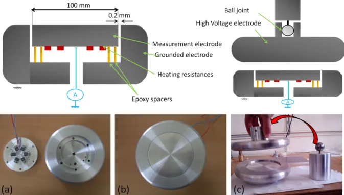
2.2 Experimental systems . . . 46
2.2.1 Small scale coaxial electrode system . . . 47
2.2.2 Large scale plane-to-plane electrode system . . . 49
2.2.3 Experimental protocols . . . 51
2.2.3.1 Electrodes . . . 51
2.2.3.2 Test cell conditioning . . . 52
2.3 Experimental results . . . 54
2.3.1 Preliminary experiments: coaxial system . . . 54
2.3.1.1 Measurements in SF6 . . . 54
2.3.1.2 Comments . . . 58
2.3.1.3 Experiments in air and influence of water . . . 60
2.3.1.4 Influence of high voltage electrode nature in positive polarity, for different pressures . . . 63
2.3.2 Discrepancies between calculated and measured RH, and influence on the current . . . 64
2.3.2.1 Example 1: Measurements in SF6 versus pressure . . . 65
2.3.2.2 Example 2: Measurement in air mixtures with temperature variations . . . 67
2.3.2.3 Discussion: The crucial influence of test cell conditioning . 69 2.3.2.4 Influence of temperature in SF6 . . . 71
2.3.2.5 Synthesis: influence of RH in SF6 and air . . . 72
2.3.3 Parallel electrodes system . . . 74
2.3.3.1 Influence of gap distance and electric field in «standard» SF6 (RH > 15% at 0.6 M P a) . . . 74
2.3.3.2 Influence of gap distance and electric field in dry SF6(RH ≤ 5% at 0.6 M P a and 1 M P a) . . . 76
2.3.3.3 Influence of pressure and Relative Humidity RH . . . 77
2.3.3.4 Comparison with measurements obtained in the coaxial system 80 2.3.3.5 Comparison with measurements in synthetic dry air . . . . 81
2.3.3.6 Influence of heating measurement electrode . . . 82
2.4 Discussion . . . 85
2.4.1 Physical mechanisms . . . 85
2.4.1.1 Fowler-Nordheim emission . . . 86
2.4.1.2 Schottky emission . . . 86
2.4.1.3 Field desorption of water . . . 87
2.4.2 Consequences on the industrial application . . . 89
2.5 Conclusions . . . 90
Bibliography . . . 91 iv
3.1.1 Transient current in insulators . . . 96
3.1.2 Volume and surface resistivities . . . 97
3.1.2.1 Volume resistivity . . . 97
3.1.2.2 Surface resistivity . . . 98
3.1.3 Dielectric strength of insulators . . . 98
3.2 Materials . . . 99
3.3 Sample conditioning . . . 100
3.3.1 Determination of the drying time . . . 100
3.3.2 Measurements of water absorption . . . 101
3.4 Surface potential decay measurements . . . 102
3.4.1 Experimental system . . . 103
3.4.2 Experimental protocols . . . 104
3.4.3 Results . . . 105
3.4.3.1 Preliminary experiments . . . 105
3.4.3.2 SPD depending on Temperature and Relative Humidity for dry materials A and B . . . 106
3.4.3.3 SPD depending sample on water content . . . 106
3.4.3.4 SPD depending on material’s composition . . . 107
3.4.3.5 Comments . . . 108
3.5 Volume resistivity measurements . . . 109
3.5.1 Experimental system . . . 109
3.5.2 Experimental protocol . . . 111
3.5.2.1 Preliminary experiments . . . 111
3.5.3 Results and discussion . . . 113
3.5.3.1 Influence of electric field and temperature on dried materials114 3.5.3.2 Influence of water content . . . 117
3.5.3.3 Simulation model . . . 118
3.5.3.4 Additional investigations: influence of the material compo-sition . . . 119
3.6 Surface resistivity measurements . . . 121
3.6.1 Experimental system and protocol . . . 121
3.6.2 Preliminary experiments: creeping discharges . . . 122
3.6.3 Results and discussion . . . 122
3.6.3.1 Surface resistivity in dry gases . . . 122
3.6.3.2 Influence of electric field and temperature . . . 123
3.6.3.3 Simulation model . . . 124
3.6.3.4 Influence of relative humidity RH of the gas . . . 128
3.6.3.5 Further investigations: surface treatment . . . 129
3.7 Conclusions . . . 132
Bibliography . . . 134
4 Numerical calculations in a GIS geometry 137 4.1 1st Step: Electric field distribution induced by the material volume resistivity139 4.1.1 Difference between AC and DC (uniform temperature 20◦C) . . . . 139
4.1.2 Influence of a temperature gradient . . . 140 v
4.2 2nd Step: implementation of non-linear surface properties . . . 146
4.2.1 Uniform Temperature . . . 147
4.2.2 Temperature gradient . . . 149
4.3 Practical consequences . . . 151
4.4 Estimation of current from the gas . . . 152
4.5 Conclusions . . . 154
Bibliography . . . 154
General Conclusions and Perspectives 155
Appendix A 158
Appendix B 160
The demand for reliable, economic and environment-friendly energy resources is increasing, especially for long distance transmission. During the last ten years, the energy production from wind turbines has strongly increased. The development of offshore wind farms brings considerable economic opportunities. Indeed, it will represent 14% of Europe electricity demand by 2030. These new energy sources are often located far from the consumption areas, thus, new technologies are required to interconnect those power grids over long distances.
Nowadays, the development of High Voltage Direct Current (HVDC) transmission lines is very promising for next networks generations, which will overcome High Voltage Alternative Current (HVAC) limitations. Gas Insulated Substations (GIS) constitute an important element of power grids. Under HVAC, it has been thoroughly developed and optimized. However, it remains really difficult to develop and optimize a reliable system under HVDC. The knowledge about the DC behaviour of both insulating solid materials and gases is essential for an optimized design and for the reliability of HVDC equipment.
The main purpose of this thesis is first to experimentally investigate conduction phenom-ena in both solid and gaseous insulators, in HVDC GIS functional conditions of use. Based on these data, the objective is to develop a numerical model to evaluate the influence of various parameters and estimate their impact on conduction phenomena in solid insulator, and hence on the electric field distribution which constitutes the basic data for design and optimization.
In chapter 1, we review the existing challenges concerning energy transmission and distribution across long distances. A comparison between Alternative Currents (AC) and Direct Currents (DC) is first presented allowing to assess the main differences between both techniques. Then, we describe the investigations performed so far in Gas Insulated Substations under HVDC. Based on the existing work, we are able to define the key parameters to investigate, in order to better understand and improve HVDC insulation technology, and propose innovative solutions.
In chapter 2, we review the state of the art of current measured through pressurized gas and vacuum, at low and high electric field. Then, we proceed with experimental measurements on current through pressurized gases in two electric field geometries, and analyze the results obtained to discuss the origins of these currents.
In chapter 3, the experimental devices used for the characterization of conduction phenomena through the solid insulator are presented. We investigate the influence of temperature, electric field and relative humidity on the conduction through the insulator volume and on its surface.
Finally, in chapter 4 we present several numerical calculations accounting for the influence of parameter investigated in a real GIS insulator geometry. The contribution of such parameters can be estimated and their impact on the conduction current and electric field distribution through the solid insulator is evaluated.
for HVDC GIS
Contents
1.1 General considerations on electrical transport and distribution . . . 3
1.2 From Alternating Current to Direct Current . . . 4
1.2.1 Technical merits of HVDC . . . 5
1.2.2 Economic and environmental considerations . . . 6
1.3 Gas-Insulated-Substations (GIS) . . . 7
1.3.1 Solid dielectrics . . . 8
1.3.2 SF6 gas . . . 9
1.4 Development and optimization of HVDC GIS . . . 10
1.4.1 Charge accumulation . . . 10 1.4.2 Influencing parameters . . . 13 1.4.3 Charge decay . . . 19 1.4.4 Simulation models . . . 22 1.5 Conclusions . . . 22 Bibliography . . . 25
In this chapter we will first present the evolution of energy distribution networks from High Voltage Alternating Current (HVAC ) transmission to High Voltage Direct Current (HVDC ). A brief description of advantages and drawbacks of these techniques is presented. The structure and operating conditions of Gas Insulated Substations (GIS) are then introduced. Some existing HVDC technologies are detailed, highlighting the main parameters to take into account to design and optimize HVDC GIS. Then, we will present the current understanding of charge accumulation and relaxation on solid insulators, which are of major importance for the reliability and optimization of HVDC technology. Finally, the main objectives and topics addressed in this work are presented.
1.1 | General considerations on electrical transport and
distribution
High power production facilities, such as nuclear, hydraulic, photo-voltaic, and wind farms power plants, are often located far away from consumers. To transport electrical energy from the source toward consumers, the entire electrical network, basically composed of
transmission networks and distribution lines, is used. Figure 1.1 shows an illustration of grid structure, with the combination of networks and substation transformers. The substation transformers are placed at each node of the network and permit converting high voltage to low voltage and vice versa. Two different types of substations can be used, Air-Insulated-Substation (AIS) and Gas-Insulated-Substation (GIS).
The transport of electrical energy presents some losses (due to Joule effects and other phenomena), notably concerning the transport over long distances. Indeed, when electricity passes through electrical cables, a certain quantity of this energy is transformed into heat due to the Joule effect. This energy loss can be reduced by increasing the voltage and decreasing the current for long distance transmission. That is why high voltage is usually employed for long distances transmission (> 100 km) while low and medium voltages are used for distribution networks (< 100 km). These three voltage levels are represented in figure 1.1.
Fig. 1.1: Schematic illustration describing the global network used to the transport of electrical energy. Transmission networks and distribution lines are interconnected through substations transformers.
Additionally to the transport of electricity, this structure permits to isolate dysfunctions on a specific section of the network without cutting-off electricity over the entire network.
1.2 | From Alternating Current to Direct Current
Two types of currents are used for energy transport: Alternating Current (AC) and Direct Current (DC). Both started many years ago, in 18800s, with the War of Currents between Thomas Edison (who was pushing for the development of DC power networks), and Georges Westinghouse, (who believed in AC power networks). At that time, DC networks were suitable and well-adapted to the consumers. However, some improvements on the AC systems
(creation of a transformer stage between the transmission network and consumer materials), allowed higher power and insulation levels within one unit. This system was simple and only required little maintenance. For these reasons, AC technology was introduced at a very early stage in the development of electrical power systems. Nevertheless, HVAC transmission technology presents some drawbacks which compelled a change to DC technology. The transmission capacity and distance of AC links are limited by inductive and capacitive phenomena occurring within overhead lines and cables. These issues are of major importance for cables longer than about 100 km since the achievable transmission will be limited by the charging current. Besides, it is not possible to directly connect two AC systems working at different frequencies.
With the development of high voltage valves, it becomes possible to transmit power at high voltages over long distances, giving rise to HVDC transmission systems. Such technology has several advantages compared to the AC transmission which make it especially attractive in certain transmission applications. HVDC systems are getting increasingly important in the global development of energy sources and networks for technical, economical and environmental reasons.
1.2.1 | Technical merits of HVDC
With an increased demand for energy and construction of new generation plants at remote locations (e.g off-shore wind farms), the complexity of power system has grown and higher voltages are needed to transmit energy across very long distances, with as low losses as possible. As inductive and capacitive parameters do not limit the transmission capacity or the maximum length of a DC cable, HVDC offers a suitable solution compared to HVAC for such power systems.
A simplified representation of a HVDC interconnection is shown in figure 1.2. A converter, operating as a rectifier will transform AC power to DC power. The latter is then transmitted and applied to the DC terminals of a second converter, which allows the DC power to flow into the receiving AC network. The composition of a HVDC system varies with the technology used in converters. However, a common structure formed by AC filters, transformers, converters, DC capacitors or reactors and DC cables, can be established. Further detailed description of HVDC systems are made in a technological paper published by Rudervall et al. [1].
Fig. 1.2: Simplified representation of HVDC interconnection between two AC networks.
1.2.2 | Economic and environmental considerations
Depending on the transmission task, feasibility studies are performed to estimate the cost of AC/DC lines according to losses and distances. Figure 1.3 shows (b) losses comparison and (a) typical cost comparison curve between AC and DC transmission, accounting for the terminal cost, line cost as well as the value of losses for each AC and DC technology. It can be observed that on the one hand, the investment costs for HVDC stations are higher than for HVAC. On the other hand, the costs of transmission medium and line per kilometer are considerably lower for DC. The distance for which total AC and DC costs are equals is named the break-even distance. It is usually in the range of 500 to 800 km, and depends on project financing, loss evaluation, cost of right of way, etc. It can be observed that for distance superior than the break-even distance, the total AC costs are higher than total DC costs considering similar transmission distances.
The desire to limit environmental impact also conducts to a HVDC transmission system. Indeed, HVDC network can transmit more power over fewer lines and hence reduce the visual impact and save land compensation for other projects. Moreover, there is no induction of alternating electro-magnetic fields from HVDC transmission, and lower underground cable losses improves efficiency.
Fig. 1.3: (a) Comparison of costs between AC and DC technologies according to transmission distances, and accounting for the terminal costs, line costs and values of losses. (b) Comparison of losses between AC and DC technologies according to transmission distances.
1.3 | Gas-Insulated-Substations (GIS)
With the evolution of high voltage and very high voltage electrical networks, the realization of substations had significantly evolved. The consumption of electrical energy is located closer to industrial or urban areas, which implied to distribute high power in regions where the space is restricted and rare. The dimensions of Air Insulated Substations (AIS) are imposed by the insulation distances in air, so the solution to make them more compact is to use a better insulating gas within an enclosure under pressure (GIS). Figure 1.4shows an illustration of an AIS (a) and a GIS (b). AIS technology requires an important area (0.5 to 2 hectares), while GIS allows reducing this area by a factor 3 or 4. With this technology, it is thus possible to transmit higher voltages close to urban sites in a compact, reliable and robust enclosure.
An illustration of GIS compartments is presented in figure 1.5. They are composed of a metallic enclosure linked to the ground (grounded vessel), a central conductor, insulating solids and gas. The conductor is isolated from the grounded enclosure using pressurized sulfur hexafluoride (SF6) and epoxy resin insulator, which has a double functionality. The
solid insulator is used to carry the conductor, and can also be used as a tight spacer which enables the separation between two compartments.
This structure, already used for HVAC systems, is of major interest for HVDC technology. Our study is based on this GIS model, and the different elements composing the GIS are detailed hereafter.
Fig. 1.4: Illustration of (a) an AIS, and (b) a GIS.
Fig. 1.5: Illustration of a junction between two compartments in a GIS.
1.3.1 | Solid dielectrics
In a GIS, solid insulators mainly constitute a mechanic support for conductors, and must also be able to transmit the heat flow between the different parts of the device.
The insulator design takes into account the applied electric field, and various constraints such as: chemical interactions with gas, mechanical and thermal constraints. Depending on the insulation requirements, various categories are existing. High voltage insulators have been first developed with ceramic and porcelain [2], and then were later changed by modern polymeric insulators [3]. First introduced in 1959, they were made of SiO2 or Al2O3 filled
epoxy resin [4]. Their design flexibility, light weight, withstands performance to pressure and their ease of handling for manufacturing, make them preferable compared to ceramics. Moreover these composite materials are safer than porcelain since they are not brittle so the risk of explosion is largely reduced.
Up to now, those materials are adapted and withstand AC voltages but are not suitable for DC technology. The challenge consisting in finding a suitable design which withstand HVDC, constitutes the basis of our study. We focused on organic synthetic insulators
(polymer composite) currently used for AC technology. The behavior of these materials under DC is totally different since electric field distribution depends on conductivities, charge accumulation, and not on permittivities anymore.
1.3.2 | SF
6gas
Sulfur hexafluoride was discovered by Moissan and Lebeau [5,6] in 1900. It is synthesized directly from sulfur and fluorine elements, with a strong exothermic reaction (262 Kcal per mole) written as, [7]:
S + 3F2 → SF6+ 262 kcal (1.1)
Since its first industrial application in 1940 (patent from Thomson-Houston in 1939), the SF6 was widely used in the field of industrial insulation due to its high dielectric strength,
and very good behaviour in circuit breakers.
SF6 is one of the heaviest known gases. With a density of 6.139 kg/m3 (at 20◦C and
0.1 M P a), it is almost five times heavier than air (146 g/mol for the SF6 and 28 g/mol for
air). As shown in figure 1.6, SF6 molecule is perfectly symmetric. It is a stable and inert
molecule.
Fig. 1.6: Illustration of a molecule of SF6.
It is an electronegative gas due to its Fluorine (F) atom, which means that it is able to capture free electrons, forming heavy ions with low mobility, and thus making the development of electron avalanches very difficult [8]. Besides, due to its high dissociation temperature (500◦C) and high dissociation energy, SF6 has excellent arc-interruption
properties.
However, the SF6 also has drawbacks, mostly concerning environment. When SF6 is in
decomposition (during strong electrical discharge), toxic and corrosive by-products such as Hydrogen Fluoride (HF) can be created. Moreover, as this gas is very stable and chemically inert, its global warming potential is approximately 24000 times higher than that of CO2.
Thus, severe conditions of use had been established in order to control the loss quantities of this gas and re-use it when no decomposition occurred.
Investigations on various alternative gases (N2, CO2, ...) are currently in progress to
replace SF6 in some parts of the GIS, or also to mix it with other gases [9–11]. Nevertheless,
up to now no other gases or techniques were found to fully replace advantages presented by SF6.
1.4 | Development and optimization of HVDC GIS
The «Kii-channel» HVDC system (±250 kV , 2800 A) was the first and largest bulk HVDC transmission system, built in Japan. It was put in commercial use in June 2000 [12]. Further investigations were conducted in order to upgrade this existing system to a capacity up to 2800 M W (±500 kV , 2800 A) [13]. In same years, ABB corporation performed a feasibility study of SF6 GIS for HVDC at 500 kV and 600 kV based on existing AC materials
(insulating parts). Finally, their long term performance required special spacers modified for DC technology [14]. Criteria for design and optimization of HVDC GIS are not well understood up to now. Thus, existing devices were over-sized to ensure a safe operation.
Several research works have been reported concerning the insulator behaviour under HVDC. These researches take into account the insulator geometry [15–17], which is shown to have a great influence on breakdown voltage level. Some studies [18,19] also underlined the predominant influence of the surface charge accumulation phenomena, which is one of the major issue in HVDC. Other experiments have also been able to evaluate the influence of the insulator’s roughness, and of the nature of the high voltage electrode used for the experiments [17]. The presence of metallic particles in a GIS has also been investigated [15]. In addition, some simulation methods have been developed [20–23]. The relevant literature concerning these issues is reviewed in the following.
1.4.1 | Charge accumulation
Under impulses and AC voltages, the voltage distribution along the insulator surface and within its volume is dependent on the dielectric constant (ε) of the insulator. In contrast, for DC voltages the situation is much more complex. The initial distribution under DC is determined by the capacitive grading. Then, over prolonged application time, the stress distribution is determined by the resistivity of the insulator. In HVDC GIS, charges can also accumulate on the insulator surface and they will introduce additional changes in the voltage distribution and lead to field distortions, that may result in the reduction of the insulator flashover voltage. Figure 1.7 shows measurements of the flashover voltage versus surface charge density. It was obtained with switching impulses applied after application of a 200 kV pre-stress, with various polarity combinations. The flashover voltage significantly
decreases with σ, especially when pre-stress and switching impulses are of opposite polarities. This confirms the major impact of charge accumulation on the insulator dielectric strength.
Fig. 1.7: Relation between charge density (measured by a non-contacting probe) and flashover voltage [22].
Both volume and surface resistivities of the material influence charge accumulation and relaxation. The actual origin of surface charges is not clearly established. The relevant literature will be analyzed in chapter 2.
In the following, we review the main parameters involved in the complex equilibrium between charge accumulation and relaxation.
1.4.1.1 Field calculations
In HVDC, a small quantity of free charges are generated in the gas (see section 2.1 in chapter 2). These charges move along the electric flux lines toward the insulator surface. If the surface resistivity is high, charge accumulation over long periods of time can occur on the insulator surface. Numerical simulations of surface charge accumulation on GIS insulator were reported by Messerer et al. [24–27]. In their work [27], they studied the phenomenon of charge accumulation on a spacer surface, using artificial charge generation with points (corona effect). These points create charges which are transported onto the insulator surface following electric field lines. Figure 1.8 shows the results of the charging process at three different time, obtained by simulation.
In their simulation, they consider that the saturated charge density is given by boundary conditions following equation1.2, where ε1 is the dielectric constant of the gas (= 1) and ε2
Fig. 1.8: Movement of charges for various charging time, (a) 0 h, (b) 53 h, and (c) 838 h [27].
the dielectric constant of the material considered.
ε1E1n− ε2E2n = σsat (1.2)
The electric field is composed of a normal (En) and a tangential (Et) components. It
is considered that charge accumulation is enhanced by normal electric field on the spacer surface whereas the tangential component helps charge relaxation and is responsible for breakdowns. The charge accumulation reduces E1n at gas side, while it enhances gradually
E2n on the insulator surface side, until a steady state is reached when the normal electric
field at the gas side equals to zero [28]. This means that the insulator is fully charged (σsat).
A similar calculation method is found in Fujinami et al. work [22]. Four types of insulators were used with various electrode diameters and metal inserts. The objective was to study the normal and tangential fields for each configuration and compare the calculated charge accumulation to experimental data after several voltage application periods. In practical cases, the electric field for a spacer in SF6 gas would change from a capacitive
distribution to a resistive one at very long times.
It is reported that for short application time (5 h), the calculated values of surface charge densities are superior to the experimental measured values (obtained using a multi-point measurement method via electrostatic probes). Results obtained after 139 h of applied voltage are shown in figure 1.9, for one type of insulator (type C).
Both calculations and measurements are in agreement when the application of voltage lasts very long time.
Charge accumulation on insulator surface is a mechanism mainly controlled by electrical field components (normal and tangential), which has a strong effect on insulator flashover and dielectric strength. To reduce the charge accumulation, the insulator shape must be optimized. The ideal geometry to avoid charge accumulation would be a geometry with only tangential electric field on insulator surface (as suggested by Fujinami [22]).
Fig. 1.9: (a) Sectional view of type C insulator, (b) charge distribution after 139 h application of DC voltage [22].
1.4.2 | Influencing parameters
1.4.2.1 Insulator shape
Several authors [15,16,22,29–31] have made researches concerning the influence of insulator shape onto the breakdown field strength under DC voltages.
An investigation led by Hasegawa et.al [32] points out the influence of the insulator shape on its dielectric strength under HVDC. Figure1.10presents the electric field evolution according to three different insulators shapes. It was observed that high tangential field are obtained for a disk spacer (a) while low tangential field and high normal field are obtained for a conical spacer. The semi-conical spacer (c) presented the best solution since it satisfied the requirements of low tangential and normal field. The optimized insulator, tested under AC and DC voltages, with lightning and switching impulse and polarity reversal, satisfied the insulation with sufficient margins.
Fig. 1.10: DC electric field distributions on spacer surface on the concave side of (a) a disk spacer, (b) a conical spacer and (c) a semiconical spacer [32].
Another investigation done by Volpov et al. [30] shows the influence of the insulator shape on the charge accumulated onto the insulator surface. Their experiments, initially performed using a 1150 kV HVAC GIS insulator, failed under long term HVDC. The authors postulate that to optimize the insulator, a maximum value of charge accumulation can be tolerated. They recommend to not exceed a normal electric field of 1 M V /m and a
tangential electric field of 3.5 M V /m. These constrains would allow to control the R-C field transition so that maximum accumulated surface charge density does not exceed 10 − 20 µC/m2, and causes no appreciable distortion in the spacer field. Figure1.11 shows
the investigated shapes with corresponding normal and tangential electric field respectively for (a) existing AC insulator and (b) optimized DC insulator. It has been observed that optimizing the insulator shape results in significantly lowering the normal component of the electric field and thus the surface charge density along the insulator surface.
Fig. 1.11: Design shape of insulator used for (a) HVAC GIS and (b) optimized shape withstanding 750 kV HVDC, and corresponding electric stress on the insulator surface [30].
According to their field requirements, they obtained a surface charge density ≤ 10 µC/m2, which led to only a slight difference between the initial and DC stabilized field distribution along the spacer surface. No abnormal reductions in the insulator electric field strength were registered at long term DC voltage application.
The study of Lorenzi et al. [31] agreed with the previous work concerning the large influence of the normal electric field component on both charge accumulation and dielectric strength variations. The main difference pointed out is the consideration of surface and volume resistivity impact on the charge accumulation. Indeed, modifying the shape of insulators allows reducing the normal component, but only for the cases in which the volume resistivity is the dominant mechanism leading to charge relaxation, compared to the surface and SF6 resistivities. In other cases, the optimization of the insulator profile may not
induce a reduction of the surface charge. In their simulation, best results were obtained with low volume resistivity in presence of a non-linear surface resistivity.
1.4.2.2 Insulation properties and charging time estimation
Charge accumulation results from an equilibrium between charges flowing onto the insulator surface (surface resistivity), through its volume (volume resistivity) and charges coming from the gas. Depending on these dynamics, different charge accumulations can be reported.
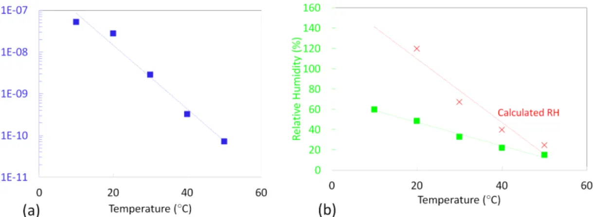
Examples of volume and surface resistivity measurements according to both electric field and temperature are shown in figure 1.12 [21]. Measurements were performed on alumina-filled epoxy resin, in SF6 with a pressure varying between 0.25 M P a to 0.35 M P a.
It was observed that both surface and volume resistivities depend on electric field and temperature. However, it seemed that the volume resistivity mainly depends on temperature, whereas surface resistivity shows a large variation versus electric field.
Fig. 1.12: (a) Volume and (b) surface resistivities according to electric field and temperature variations [21].
To explain the basic mechanism of charging insulator surfaces, the properties of the insulating gas must be also considered. However, it is very difficult to estimate the influence of the gas since charge generation processes are not clearly identified. Charges can presumably be due to natural ionization, field emission from electrode surfaces, charged particles within gas, and partial discharges (corona discharges). In their work, Kumada et al. [33] calculated a virtual «volume resistivity» of air only considering the charge carriers generated by natural ionization. Then, considering that the number of charge carriers in air can also be influenced by micro-discharges or field emission from the conductors, they considered a volume resistivity ratio of the gas ρg to the insulator ρs in order to estimate the
charge density accumulated on the insulator, as well as its charging time. Those calculations are presented in figure 1.13.
Fig. 1.13: Numerical calculation of charge density distribution along a conical slope spacer [33].
1.4.2.3 Influence of insulator surface roughness
Some works have reported the influence of insulator surface roughness on charge accumula-tion [16,21,22]. The roughness may slow down or enhance the surface charge decay, and thus modify the dielectric properties of insulators.
Fujinami et al. showed in their work [22] that charge density is higher when surface roughness is larger. This result was also verified by Iwabuchi et al. [34] on an epoxy disk spacer presenting a flat and an inclined surface. Figure 1.14 shows a schematic view of the insulator partly roughened by sand blasting (a) and a charge distribution measured on the flat surface of this insulator (b).
Fig. 1.14: (a) Schematic view of the insulator with an area roughened by sand blasting, and (b) charge distribution measured on the flat surface of the corresponding insulator after 240 h of voltage application (30 kV on the central conductor) [34].
In their experiment, HVDC was applied for a long time on this sand blasted insulator (240 h). It can be observed that the higher surface charge concentration is localized on the boundary of the roughened region (figure 1.14(b)). Authors assume that the roughness has an indirect impact on charge accumulation. After sand blasting, fillers of the insulator appeared on the insulator surface, resulting in a non-uniformity of surface resistivity along the insulator. This non-uniformity of surface resistivity is assumed to provoke charge accumulation.
1.4.2.4 Influence of electrode surface coating
Charges in the gas can be presumably created due to micro-protrusion on the grounded vessel or on electrode surfaces. Some studies were performed by Endo et al. [35], Menju et al. [17] and Okabe et al. [21] concerning the possible effect of a coating on electrodes, in order to reduce the charge emission.
Coated electrodes have been tested, assuming that an insulating polymer coating may reduce the effect of micro-protrusions, and then increase the breakdown field strength (EBD).
Work of Yoshida et al., reported in [21] is presented in table 1.1 and figure 1.15.
N◦ Electrode Coating Insulator Coating Insulator Surface Resistivity [Ω]
(1) None None 1016− 1017
(2) None Epoxy (300 − 800 µm) 1014− 1015
(3) Epoxy None 1016− 1017
Tab. 1.1: Summary of the experimental conditions, describing electrode and epoxy insulator surface condition presented in figure 1.15.
It is observed that with a dielectric coating on the electrode, the surface charge density measured is significantly lowered (close to 1 nC/cm2). Thus, the charge density measured
in case of N◦1 and N◦2 was assumed to be due to field emission. In their experiment, the surprising higher charge density obtained in case N◦2 compared to N◦1 is not explained. Indeed, it is well known that the lower the surface resistivity, the lower the charge density. A complementary investigation [17] showing the evolution of the breakdown field strength in a coaxial geometry with coated and un-coated anode and cathode electrodes is presented in figure1.16. It is observed that for un-coated electrodes, positive EBDis close to theoretical
values while the negative value is lower. Then, coating the cathode electrode in negative polarity results in an increase of EBD. Besides, in positive polarity, no influence of the
electrode coating is observed. This strongly suggests that the decrease of EBD observed
without coating was due to field emission from micro-protrusion on the cathode.
To avoid field emission from tips present onto electrodes, a dielectric coating is recom-mended onto the negative electrode, or a good polishing is recomrecom-mended. However, Hairour
Fig. 1.15: Measurements of charge density over time for three different spacer surface and electrode conditions presented in table 1.1 [21].
Fig. 1.16: Effect of electrode coating on DC breakdown voltages in SF6, for a coaxial
geometry [17].
et al. [36] also investigated the influence of the breakdown field strength in presence of a coating onto the conductor. They evidenced that a dielectric coating results in a lower average of the breakdown field strength in both polarities. Thus, further work should be performed in order to reduce the charge injected from the conductor, without reducing the breakdown field strength.
1.4.2.5 Metallic particles
Dust and conducting particles may be present within GIS, and might deteriorate the dielectric performance of the system. Several investigations were performed [32,33,37–40] to determine the impacts of those particles on the electric breakdown voltage, and on the
charge accumulation. It is known that in GIS, both free and attached particles can trigger breakdown. The influence of particles will vary with their nature (dielectric or conductive), shape and dimensions, location and orientation within the system. Those influences were detailed by Cookson et al. [37,39].
It is reported that for a DC field, a particle (in the absence of corona) is driven across the gap electrodes until it strikes the opposite electrode, where it is oppositely charged, and driven back to repeat the motion and oscillate between the electrodes. In the case of negative polarity, particles float around the high voltage conductor, which is called «firefly» phenomenon. During their random movement, particles may attach themselves to the insulator, and greatly decrease its insulation strength. To increase insulation reliability of DC GIS, a system allowing to remove particles should be developed.
Hasegawa et al. [32] proposed a new GIS design including a particle trap, and a particle driver presented in figure 1.17(a).
Fig. 1.17: Illustration of a basic insulation structure of a GIS including a particle trap system (a), and experimental results showing the efficiency of a particle driver at DC −250 kV , and with 3 mm long aluminum particles (b). [32].
In their device, a particle driver is placed on both high-voltage conductor side, and onto the vessel allowing to drive the particles into the trap. Moreover, an additional shielded ring named «field-well» ring was positioned at the end of the particle drivers to get rid of fireflies phenomena for electric field lower than 2 M V /m. Figure 1.17(b) shows the relative number of particles attached on the insulator, fire-flying within the gas and trapped. It was observed that if neither the particle driver nor the field-well ring were present, 50 % of particles were trapped, while with both systems all particles were successfully trapped.
1.4.3 | Charge decay
The charge accumulated on the insulator surface can decay following three mechanisms: electric conduction along the insulator surface, through its volume, and charge neutralization by gas ions. This phenomenon had been widely investigated [18,19,41–44] on various materials and for different conditions, using Surface Potential Decay (SPD) measurements.
SPD (detailed in [18]) consists in a deposition of charges created by corona discharge, on a localized area of the insulator surface. Once charges are deposed, the potential on this charged area is measured versus time. This technique allows investigating the dynamics of charge versus various parameters (RH, time, charge deposited). Hereafter, only the influence of relative humidity and surrounding gas are presented to point out the possible influence of such parameters in the real application. However, it is worth noting that the correlation between potential decay measurements and real case in GIS is questionable since rather different conditions and geometries are used.
1.4.3.1 Influence of relative humidity
The effect of gas Relative Humidity (RH) and water absorption by the solid on surface charge decay and volume resistivity had been studied by few authors [18,45–48].
It has been demonstrated on different materials (epoxy resin, quartz and PTFE) that the electrical properties of the insulator surface depended on the amount of adsorbed water vapor. Figure 1.18shows the surface resistivity variations obtained at different RH in case of epoxy resin by Crisci and Lutz [18,47]. Those results evidence that with increasing RH, up to 80%, surface resistivity dramatically decreases.
Fig. 1.18: Surface resistivity variations of an epoxy resin with relative humidity [18,47].
In both studies, by increasing RH from 55% to 65%, the surface resistivity decreases by one order of magnitude. It is then deduced that the humidity can play an important role on the surface potential decay at rather high values of RH. It is worth noting that no investigations have been performed with low RH (≤ 30%) so far. According to Awakuni et al. [46], water molecules adsorbed on the insulator surface contribute to the surface conduction. In their work, it is reported that the surface resistivity exponentially decreases with the number of water molecules layers.
In addition, volume resistivity measurements have also been performed [45,48]. The results show that with increasing water concentration within the solid, its volume resistivity significantly decreases.
1.4.3.2 Influence of surrounding gas
An investigation led by Kindersberger et al. [20,49] evidences the influence of the surrounding gas on potential decay experiments. It has been shown that the charge can be neutralized by the gas ions. These ions are generated by natural radiation. Only ions, generated within a certain volume around the charged area (where the electric field strength is high enough to prevent recombination), can contribute to charge neutralization. Figure 1.19 shows the surface potential distribution directly after charge deposition (a) and after 660 min (b).
Fig. 1.19: Surface potential distribution on epoxy resin (a) immediately after charge deposition, (b) after 660 min [49].
Depending on the surface potential distribution shape, the mechanism responsible for the decay can be identified. If the «bell» shape obtained just after charge deposition remains during decay, no influence of gas neutralization is observed, whereas when a crater-like shape is observed, this strongly suggests the charge neutralization by gas ions. Comparing their results with a simulation model which accounts for charge neutralization by gas ions, they were able to confirm this assumption. Thus, depending on the solid insulator material, the conditions and properties of the surrounding gas near the charged area, and the electric field applied in such device, the charge decay may be significantly influenced by the surrounding gas. However, this neutralization mechanism cannot be directly extrapolated to the real application. Indeed, in such experiments, a charge is deposed onto the insulator surface by a corona discharge. Then, immediately after charge deposition, the surface potential is measured. In this case, charges on the insulator surface create the electric field distribution and neutralization by gas is possible. This is not the case in the real application, where the applied electric field brings charges of the same polarity than those present on the insulator
surface. In such conditions, the neutralization by the surrounding gas cannot occur.
1.4.4 | Simulation models
Various simulation models have been developed around phenomena involved in the charge accumulation.
Some models [21,33] developed a simulation tool which enables to estimate the charge on the insulator based on potential measurements along the insulator surface.
In [22–24,30,50], models taking into account the variations of volume and surface resistivities with electric field were developed, considering solid and gaseous dielectrics to be linear media. Such models allow describing the evolution of the electric field for various types of insulators and estimate the charge accumulation along the insulator surface. Based on those calculations, critical values for the maximum charge accumulated on the surface, and also for the normal and tangential components of the applied electric field have been determined (10 − 20 µC/m2) [30].
However, in the above quoted models, the phenomena of charge transport through gas were not considered. Volpov et al. recommend accounting for the processes of ion generation, recombination and ion drift in compressed gases to establish a correct model. Another simulation work reported by Kindersberger et al. [20] presents a simulation tool describing the charge decay on a solid dielectric accounting for electric conduction of both surface and volume, and also charge neutralization by gas ions. In their work, the influence of gas was implemented in the model by calculating the ion pair generation by natural ionization in their experimental devices. Then, based on this ion pair generation rate, the resulting current density in electric field was estimated.
The existing models permit evidencing the influence of the insulator shape, electric field orientation and solid and gaseous dielectric properties on the mechanism of charge accumulation. However, up to now, no model describes those phenomena altogether. Furthermore, additional mechanisms such as charge injected from the electrode surface may also be considered in the simulation of charge accumulation.
1.5 | Conclusions
In this chapter, we have reviewed nowadays challenges which make HVDC GIS an attractive technology for long distance transmission compared to AC technologies. Concerning HVDC GIS insulation optimization, the charge accumulation mechanism occurring on the surface of the dielectric solid has been mainly considered. The principal phenomena involved in charge accumulation and relaxation have been detailed. It has been shown that charge accumulation is strongly dependent on the electric field component orientation (normal
and tangential field). Based on numerical calculations considering the components of the electric field, the insulator shape can be modified in such a way that charge accumulation could be reduced.
In addition, the electric field distribution (and hence the charge accumulation) also depends on the solid dielectric properties (surface and volume resistivities). Those properties vary with the temperature, electric field, presence of water, but rather few works were devoted to study the influence of these parameters.
Hence, the charge accumulation results in a complex equilibrium between electrical conduction through the volume and on the surface of the dielectric solid, as well as charge generation and transport through the dielectric gas. To reduce this charge accumulation, it has been suggested to:
−→ Add a dielectric coating on the high voltage electrode surface to reduce the charge injection,
−→ Implement a semi-conductive layer on the insulator surface to adjust its resistivity, −→ Optimize the insulator shape,
−→ Reduce particle contamination within the device by the implementation of particles traps.
However, those recommendations are not sufficient to allow the development and optimization of a reliable HVDC GIS. It is then reasonable to suppose that other phenomena and parameters, not yet investigated, may have an important contribution to the charge accumulation. Hence, the purpose of this thesis is twofold. On the one hand we will investigate the charge generation process within the insulating gas, and on the other hand we will develop a numerical model allowing to estimate the electric field distribution and calculate the leakage current through the solid insulator.
In chapter 2, we will first review the state of the art of charge generation processes in gas and vacuum. Then, we will focus on two main questions:
1) The possible origins of those charges, 2) The parameters influencing those charges.
Thus, we will develop experimental test setup allowing to precisely measure low cur-rents under HVDC (up to 250 kV ) and characterize these curcur-rents according to different parameters.
Afterwards, a numerical model will be developed (chapter 4) in order to evaluate the modification of electric field distribution and leakage current in presence of different parameters. In a GIS, the conductor is often at higher temperature than the vessel, resulting in a temperature gradient along the solid insulator. The influence of this temperature
gradient on the field distribution was not reported up to now. In addition, the presence of water within solid insulator will be evidenced in chapter 3. The latter will also be implemented within the model.
The model is based on characterization of solid insulators physical properties, using typical conditions of GIS (SF6environment, and electric field up to 5 kV /mm). Experimental
test setups able to measure low-noise currents under high voltages and different temperatures will be developed and presented. Hence, solid dielectric will be characterized in conditions relevant of GIS (in pressurized SF6 at high electric field), with a good control of sample
Bibliography
[1] R. Rudervall, J. Charpentier, and R. Sharma, “High voltage direct current (hvdc) transmission systems technology review paper,” Energy week, vol. 2000, 2000. (cited in page 5)
[2] J. Holtzhausen, “High voltage insulators,” in Electrical IDC technologies. (cited in page 8)
[3] T. Sorquist and A. Vlastos, “Outdoor polymeric insulators long-term exposed to hvdc,” in Transmission and Distribution Conference, 1996. Proceedings., 1996 IEEE, pp. 135–142, IEEE, 1996. (cited in page 8)
[4] J. Kuffel, E. Kuffel, and W. S. Zaengl, High voltage engineering fundamentals. Newnes, 2000. (cited in page8)
[5] M. H, “Action d’un courant ´electrique sur l’acide fluorhydrique anhydre,” pp. 102–1544, 1886. (cited in page 9)
[6] M. H, “Sur la d´ecomposition de l’acide fluorhydrique par un courant ´electrique,” pp. 103– 202, 1886. (cited in page9)
[7] W. C. Schumb and E. L. Gamble, “The preparation of sulfur hexafluoride and some of its physical properties,” Journal of the American Chemical Society, vol. 52, no. 11, pp. 4302–4308, 1930. (cited in page 9)
[8] L. G. Christophorou, J. K. Olthoff, and R. J. Van Brunt, “Sulfur hexafluoride and the electric power industry,” Electrical Insulation Magazine, IEEE, vol. 13, no. 5, pp. 20–24, 1997. (cited in page 9)
[9] A. Winter, J. Kindersberger, M. Tenzer, V. Hinrichsen, L. Zavattoni, O. Lesaint, R. Muhr, and D. Imamovic, “Solid/gaseous insulation systems for compact hvdc solutions,” CIGRE, pp. 8–9, 2014. (cited in page 10)
[10] H. Looe, J. Yan, and J. Spencer, “Development of a non-sf 6 self-blast type interrupter unit,” in Gas Discharges and Their Applications, 2008. GD 2008. 17th International Conference on, pp. 117–120, IEEE, 2008. (cited in page 10)
[11] K. Bousoltane, Alternatives au SF6 dans le disjoncteur haute tension. PhD thesis, Th`ese de doctorat de l’universit´e de Provence–Aix–Marseille 1, 2008. (cited in page10) [12] T. Shimato and al., “The kii channel hvdc link in japan,” CIGRE 14-106, 2002. (cited
in page10)
[13] M. Shikata, K. Yamaji, M. Hatano, E. Tsuchie, H. Takeuchi, and K. Inami, “Develop-ment and design of dc-gis,” Electrical Engineering in Japan, vol. 129, no. 2, pp. 51–61, 1999. (cited in page 10)
[14] M. Mendik, S. Lowder, and F. Elliott, “Long term performance verification of high voltage dc gis,” in Transmission and Distribution Conference, 1999 IEEE, vol. 2, pp. 484–488, IEEE, 1999. (cited in page 10)
[15] T. Hasegawa, K. Yamaji, M. Hatano, H. Aoyagi, Y. Taniguchi, and A. Kobayashi, “Dc dielectric characteristics and conception of insulation design for dc gis,” Power Delivery, IEEE Transactions on, vol. 11, no. 4, pp. 1776–1782, 1996. (cited in pages10 and 13)
[16] Z. Jia, B. Zhang, X. Tan, and Q. Zhang, “Flashover characteristics along the insulator in sf6 gas under dc voltage,” in Power and Energy Engineering Conference, 2009. APPEEC 2009. Asia-Pacific, pp. 1–4, IEEE, 2009. (cited in pages10,13 and 16) [17] H. Hama, F. Endo, S. Okabe, J. Kindersberger, K. Juhre, S. Meijer, and U. Schichler,
“Gas insulated systems for hvdc: Dc stress at dc and ac systems,” CIGRE Task force D1.03.11105, 2011. (cited in pages 10, 17and 18)
[18] A. Crisci, B. Gosse, J. Gosse, and V. Ollier-Dur´eault, “Surface-potential decay due to surface conduction,” EPJ Applied physics, vol. 4, pp. 107–1116, 1998. (cited in pages 10, 19,20 and 129)
[19] P. Molini´e, “Measuring and modeling transient insulator response to charging: the contribution of surface potential studies,” Dielectrics and Electrical Insulation, IEEE Transactions on, vol. 12, no. 5, pp. 939–950, 2005. (cited in pages 10and 19)
[20] J. Kindersberger and C. Lederle, “Surface charge decay on insulators in air and sulfurhexafluorid-part i: Simulation,” Dielectrics and Electrical Insulation, IEEE Transactions on, vol. 15, no. 4, pp. 941–948, 2008. (cited in pages 10,21 and 22) [21] S. Okabe, “Phenomena and mechanism of electric charges on spacers in gas insulated
switchgears,” Dielectrics and Electrical Insulation, IEEE Transactions on, vol. 14, no. 1, pp. 46–52, 2007. (cited in pages10, 15, 16,17,18, 22, 41, 114 and 124)
[22] H. Fujinami, T. Takuma, M. Yashima, and T. Kawamoto, “Mechanism and effect of dc charge accumulation on sf 6 gas insulated spacers,” Power Delivery, IEEE Transactions on, vol. 4, no. 3, pp. 1765–1772, 1989. (cited in pages 10,11,12, 13, 16and 22) [23] E. Volpov, “Electric field modeling and field formation mechanism in hvdc sf 6 gas
insulated systems,” Dielectrics and Electrical Insulation, IEEE Transactions on, vol. 10, no. 2, pp. 204–215, 2003. (cited in pages 10, 22,30 and 31)
[24] F. Messerer and W. Boeck, “Field optimization of an hvdc-gis-spacer,” in Electrical Insulation and Dielectric Phenomena, 1998. Annual Report. Conference on, vol. 1, pp. 15–18, IEEE, 1998. (cited in pages 11 and 22)
[25] F. Messerer and W. Boeck, “Gas insulated substation (gis) for hvdc,” in Electrical Insulation and Dielectric Phenomena, 2000 Annual Report Conference on, vol. 2, pp. 698–702, IEEE, 2000. (cited in page 11)
[26] F. Messerer, W. Boeck, H. Steinbigler, and S. Chakravorti, “Enhanced field calculation for hvdc gis,” in Gaseous Dielectrics IX, pp. 473–483, Springer, 2001. (cited in page11) [27] F. Messerer, M. Finkel, and W. Boeck, “Surface charge accumulation on hvdc-gis-spacer,”
in Electrical Insulation, 2002. Conference Record of the 2002 IEEE International Symposium on, pp. 421–425, IEEE, 2002. (cited in pages 11and 12)
[28] S. Sato, W. Zaengl, and A. Knecht, “A numerical analysis of accumulated surface charge on dc epoxy rrsin spaces,” Electrical Insulation, IEEE Transactions on, no. 3, pp. 333–340, 1987. (cited in page 12)
[29] T. Nitta and K. Nakanishi, “Charge accumulation on insulating spacers for hvdc gis,” Electrical Insulation, IEEE Transactions on, vol. 26, no. 3, pp. 418–427, 1991. (cited in page13)
[30] E. Volpov, “Dielectric strength coordination and generalized spacer design rules for hvac/dc sf 6 gas insulated systems,” Dielectrics and Electrical Insulation, IEEE Trans-actions on, vol. 11, no. 6, pp. 949–963, 2004. (cited in pages 13, 14,22 and 130) [31] A. De Lorenzi, L. Grando, R. Gobbo, G. Pesavento, P. Bettini, R. Specogna, and
F. Trevisan, “The insulation structure of the 1mv transmission line for the iter neutral beam injector,” Fusion Engineering and Design, vol. 82, no. 5, pp. 836–844, 2007. (cited in pages 13and 14)
[32] T. Hasegawa, K. Yamaji, M. Hatano, F. Endo, T. Rokunohe, and T. Yamagiwa, “Development of insulation structure and enhancement of insulation reliability of 500 kv dc gis,” Power Delivery, IEEE Transactions on, vol. 12, no. 1, pp. 194–202, 1997. (cited in pages 13,18 and 19)
[33] A. Kumada and S. Okabe, “Charge distribution measurement on a truncated cone spacer under dc voltage,” Dielectrics and Electrical Insulation, IEEE Transactions on, vol. 11, no. 6, pp. 929–938, 2004. (cited in pages 15, 16, 18and 22)
[34] H. Iwabuchi, T. Donen, S. Matsuoka, A. Kumada, K. Hidaka, M. Takei, and Y. Hoshina, “Influence of surface-conductivity distribution on charge accumulation of gis insulator under dc field,” Int’l. Sympos. High Voltage Engineering ISH, Hannover, Germany, Paper D-031, 2011. (cited in page 16)
[35] F. Endo, T. Kichikawa, R. Ishikawa, and J. Ozawa, “Dielectric characteristics of sf6 gas for application to hvdc systems,” Power Apparatus and Systems, IEEE Transactions on, no. 3, pp. 847–855, 1980. (cited in pages 17, 36,37, 38, 40and 41)
[36] M. Hairour, Etude di´electrique d’une isolation hybride gaz-solide pour appareillage haute tension. PhD thesis, Universit´e Montpellier II-Sciences et Techniques du Languedoc, 2007. (cited in page18)
[37] A. H. Cookson, “Electrical breakdown for uniform fields in compressed gases,” in Proceedings of the Institution of Electrical Engineers, vol. 117, pp. 269–280, IET, 1970. (cited in pages 18and 19)
[38] A. Moukengue Imano, R. Schurer, and K. Feser, “The influence of a conducting particle on a spacer on the insulation properties in sf6/n2 mixtures,” in IEE conference publication, pp. 3–232, Institution of Electrical Engineers, 1999. (cited in page 18) [39] C. M. Cooke, R. E. Wootton, and A. H. Cookson, “Influence of particles on ac and dc
electrical performance of gas insulated systems at extra-high-voltage,” Power Apparatus and Systems, IEEE Transactions on, vol. 96, no. 3, pp. 768–777, 1977. (cited in pages 18and 19)
[40] H. Anis and K. Srivastava, “Free conducting particles in compressed gas insulation,” Electrical Insulation, IEEE Transactions on, no. 4, pp. 327–338, 1981. (cited in page18) [41] M. Pepin and H. Wintle, “Charge injection and conduction on the surface of insulators,”
Journal of applied physics, vol. 83, no. 11, pp. 5870–5879, 1998. (cited in page 19) [42] P. Llovera and P. Molini´e, “New methodology for surface potential decay measurements:
application to study charge injection dynamics on polypropylene films,” Dielectrics and Electrical Insulation, IEEE Transactions on, vol. 11, no. 6, pp. 1049–1056, 2004. (cited in page 19)
[43] T. Sonnonstine and M. Perlman, “Surface-potential decay in insulators with field-dependent mobility and injection efficiency,” Journal of Applied Physics, vol. 46, no. 9, pp. 3975–3981, 2008. (cited in page 19)
[44] H. Wintle, “Surface-charge decay in insulators with nonconstant mobility and with deep trapping,” Journal of Applied Physics, vol. 43, no. 7, pp. 2927–2930, 2003. (cited in page19)
[45] B. Lutz and J. Kindersberger, “Influence of absorbed water on volume resistivity of epoxy resin insulators,” in Solid Dielectrics (ICSD), 2010 10th IEEE International Conference on, pp. 1–4, IEEE, 2010. (cited in pages 20,21 and 117)
[46] Y. Awakuni and J. Calderwood, “Water vapour adsorption and surface conductivity in solids,” Journal of Physics D: Applied Physics, vol. 5, no. 5, p. 1038, 1972. (cited in page 20)
[47] B. Lutz and J. Kindersberger, “Influence of relative humidity on surface charge decay on epoxy resin insulators,” in Properties and Applications of Dielectric Materials, 2009. ICPADM 2009. IEEE 9th International Conference on the, pp. 883–886, IEEE, 2009. (cited in pages 20and 129)
[48] D. K. Das-Gupta, “Electrical properties of surfaces of polymeric insulators,” Electrical Insulation, IEEE Transactions on, vol. 27, no. 5, pp. 909–923, 1992. (cited in pages 20 and 21)
[49] J. Kindersberger and C. Lederle, “Surface charge decay on insulators in air and sulfurhexafluorid-part ii: measurements,” Dielectrics and Electrical Insulation, IEEE Transactions on, vol. 15, no. 4, pp. 949–957, 2008. (cited in page 21)
[50] E. Volpov, “Hvdc gas insulated apparatus: electric field specificity and insulation design concept,” Electrical Insulation Magazine, IEEE, vol. 18, no. 2, pp. 7–36, 2002. (cited in page22)
electric field
Contents
2.1 Review of charge generation in pressurized gases and vacuum . . . 30
2.1.1 Natural ionization in gases at low electric field . . . 30
2.1.2 Charge emission mechanisms in vacuum at high electric field . . . . 32
2.1.3 Dark currents through pressurized gases (Air and SF6) at high
electric field . . . 36
2.1.4 Influence of several parameters on current measured in vacuum at high electric field . . . 39
2.1.5 Influence of the introduction of low pressure gases in vacuum experi-ments . . . 44
2.1.6 Discussion and objectives of the study . . . 45
2.2 Experimental systems . . . 46
2.2.1 Small scale coaxial electrode system . . . 47
2.2.2 Large scale plane-to-plane electrode system . . . 49
2.2.3 Experimental protocols . . . 51
2.3 Experimental results . . . 54
2.3.1 Preliminary experiments: coaxial system . . . 54
2.3.2 Discrepancies between calculated and measured RH, and influence on the current . . . 64
2.3.3 Parallel electrodes system . . . 74
2.4 Discussion . . . 85
2.4.1 Physical mechanisms . . . 85
2.4.2 Consequences on the industrial application . . . 89
2.5 Conclusions . . . 90
Bibliography . . . 91
As explained in Chapter 1, in the case of HVDC GIS technology, the charge generation, accumulation and relaxation on solid insulators are important mechanisms influencing the dielectric strength of the system. It has also been mentioned that the origin of charges coming from the gas is not well known, as well as the parameters influencing the charge generation. The objective of this chapter is to get a better knowledge on these processes, by trying to experimentally measure the currents flowing through the gas at high electric field.
We will first review the state of the art about currents measured through pressurized gases and vacuum for high applied electric fields. The current measured may have different

![Fig. 1.13: Numerical calculation of charge density distribution along a conical slope spacer [33].](https://thumb-eu.123doks.com/thumbv2/123doknet/14718934.750793/27.892.244.647.113.418/numerical-calculation-charge-density-distribution-conical-slope-spacer.webp)
![Fig. 1.15: Measurements of charge density over time for three different spacer surface and electrode conditions presented in table 1.1 [21].](https://thumb-eu.123doks.com/thumbv2/123doknet/14718934.750793/29.892.272.632.113.386/measurements-charge-density-different-surface-electrode-conditions-presented.webp)
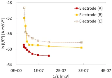
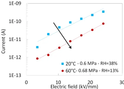
![Fig. 2.8: Fowler-Nordheim plots of dark currents obtained in 0.4 M P a of SF 6 [20].](https://thumb-eu.123doks.com/thumbv2/123doknet/14718934.750793/49.892.264.627.114.420/fig-fowler-nordheim-plots-dark-currents-obtained-sf.webp)
![Fig. 2.10: F N for current measured in air depending on electric field strength for a plane to plane electrode system [24].](https://thumb-eu.123doks.com/thumbv2/123doknet/14718934.750793/50.892.308.583.270.620/current-measured-depending-electric-field-strength-plane-electrode.webp)