Ministry of Higher Education and
Scientific Research
Promotion 2017/2018
University of Akli Mohand Oulhadj -BOUIRA
Faculty of Sciences
Department of Physics
Presented for the diploma of:
MASTER
OPTION
Physics of materials
THEME
Presented by: Kermia Aissat Amina
Before the jury:
President: Dr. ZAHAM Bouzid
MCB University of Bouira
Reporter: Dr. Bouhdjer Lazhar
MCA University of Bouira
Examiner: M. MAHDID Saida
MAA University of Bouira
Determination of the Hall coefficient of a
Germanium doped p
THANKS
I thank ALLAH the Almighty for giving me the courage, the will, and
the patience to complete this work. Also, I would like to thank the jury
for accepting to evaluate this modest work. I would like to express my
gratitude to my memory supervisor Mr. BOUHDJER lazhar. I thank
him for supervising, guiding, helping and advising me.
I would also like to thank my committee members: Dr ZAHAM
Bouzid as a president of the jury and M.
MAHDID
Saida as examiner.
In addition, I express my sincere thanks to all the teachers, speakers
and all the people who by their words, their writings, their advice and
their critics guided my reflections and agreed to meet me and answer
to my questions during my research. Thank you for the time they were
kind enough to give me and the referrals they gave me. To all these
speakers, I offer my thanks, my respect and my gratitude.
Dedications
I dedicate this modest work:
To my very dear parents who have always supported me in waiting for my goals.
As I think it will not be enough to thank them, but to satisfy them, and to give back some of their best because my joy depends on their joy.
To my husband fathi and his family. To my sister and brothers.
To my supervisor Dr: Bouhdjer lazhar and my colleagues for their precious advice who accompanied me throughout my work, who have in me a great confidence, and for the unforgettable moments that we lived together.
To all my friends.
Finally, I hope that this report will give satisfaction to all those who will have the opportunity to read it.
Table of illustrations
Chapter I :Growth Techniques Of Semiconductors
Figure I-1: crystal of pure silicon atoms………..…………..………...03
Figure I-2: structure of silicon doped by phosphorous atom having N-type semiconductor………...……….04
Figure I-3: donor ionization energy levels. ………...…..……….……...05
FigureI-4: structure of silicon doped by boron atom Having P-type semiconductor……….………...05
Figure I-5: Acceptor ionization energy levels……….………..….... 06
Figure I-6: Schematic setup of the Czochralski process………...07
Figure I-7: Growth equipment……….…....…...07
Figure I-8: AlSb single crystal obtained by a CZ process………...07
Figure I-9: Schematic setup of the Bridgman process……….……..……..….... 08
Figure I-10: Growth equipment………...….…...08
Figure I- 11: Schematic setup of the Float Zone (FZ) process……….…………...09
Chapter II: Basic Theory Of Semiconductors Figure II-1: the discrete energy states of atoms(a)are replaced by the energy bands in crystal(b) ………..………...12
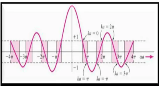
Figure II-2: A: periodic potential in a one-dimensional crystal, B: The Kronig–Penney model for a 1-D periodic lattice………...14
Figure II-3: Graphical solution of the compatibility equation (P/qa) sin qa + cos qa = cos ka of the Kronig-Penney model. ……….……...17
Figure II-4: representation of the bands energies……….…….…17
Figure II-5: the energy as function of k………...…...18
Figure II-6: Energy as a function of k, repeated with 2 a b
. The first zone of Brillouin (ZB) is represented in gray……….…....…..…...18Figure II-7: parabolic approximation for E-k diagram in the conduction band...….……...21
Figure II-9: graphic representation of density of state for a semiconductor type-n………...23
Figure II-10: graphic representation of density of state for a semiconductor type-p……...24
Figure II-11: Position of Fermi level for an (a) n-type and (b) p-type semiconductor…...27
Figure II-12: Drift of a carrier due to an applied electric field………..29
Figure II-13:Random motion of carriers in a semiconductor with and without an applied electric field………...…...……...…..30
Figure II-14: Hall Effect geometry in sc type n and sc type p………...…….….32
Figure II-15: carriers concentration gradient and the resulting diffusion currents…...…34
Chapter III:Results And Discussions Figure III-1: Materials of manipulation………..…37
Figure III- 2: P-doped germanium on plug-in board………..……38
Figure III-3 : Variation of UH(v) as a function of B(T)………..……39
Figure III-4: Hall voltage UH as function of the current I………...43
Contents
General Introduction………...01
Chapter I: Growth Techniques Of Semiconductors I-1-Introduction………...03
I-2- types of doping of semiconductor………...03
I-2-A-The intrinsic semiconductor: ………...03
I-2-B-Extrinsic semiconductors……….…03
I-2-B-1-n-type………04
I-2-B-2- p-type semiconductor……….………..…05
I-3-Growth Techniques……… …….……… 06
I-3-A-Czochralski Method……… 06
I-3-B-Bridgman Method……….... 08
I-3-C-The float zone method………... 09
I-4-Conclusion………...…….10
Chapter II:Basic Theory Of Semiconductors II-I-Introduction……….……11
II-II -Energy band theory……….……..12
II-II-1-Energy band model……….……13
II-II-2-The free electron model……….……….14
II-II-3-Periodic potentials……….….……….13
II-II-4-The Effective Mass Concept………..………...…..19
II-II-4-1-Effective Mass Tensor………..………...…21
II-II-4-2-Sign of effective mass……….…...….….21
II-III-1-Carrier Concentration and Fermi Level………...…..…22
II-III-2-Mass action law……….…...24
II-III-3-Ionization of impurity atoms in the extrinsic semiconductors………..….25
II-III-4-Position of Fermi level……… …..…27
II-IV-Semiconductor hors equilibrium………...…...….29
II-IV-1-The Hall Effect……… …………..…32
II-IV-1-1_Hall Effect and Mobility………..….….33
II-IV-1-2-Diffusion current………...33
II-IV-1-3-Einstein relationships………..……. .35
II-V-Conclusion………...36
Chapter III :Results And Discussions III-1-Objective of the experiment………...…..37
III-2-Manipulation………...…...38
III-3-Measuring the Hall voltage as a function of magnetic field…………..…... 38
III-4-Measuring the Hall voltage as a function of current……….…….... 40
III-5-Measuring the Hall voltage as a function of temperature.………...…..43
General Introduction
2
Solid materials can be classified into three groups: insulators, semiconductors and conductors. Insulates are considered to be conductivity materials (diamond 10-14 S/cm), such as semiconductor materials such as (silicon 10-5 S/cm at 103S/cm) and as conductor materials such as (silver106S/cm), the electrical properties of a material are a function of the electronic populations of the different allowed bands. Electrical conduction results from the movement of electrons within each band. Under the action of the electric field applied to the material, the electron acquires a kinetic energy in the opposite direction of the electric field. Now consider a band of empty energy, it is obvious by the fact that it does not contain electrons, it does not participate in the formation of an electric current. It's the same for a full band.
In reality, an electron can move only if there is a free space (a hole) in its energy band. Thus, a material whose energy bands are empty or solid is an insulator. Such a configuration is obtained for gap energies greater than ~ 9eV, because for such energies, the thermal agitation at 300K can not pass the electrons of the valence band to the conduction by breaking electron bonds. The bands of energy are thus all empty or all fail. A semiconductor is an insulator for a temperature of 0K. However, this type of material having a gap energy of less than the insulator (~ 1eV) well, due to thermal agitation (T = 300K), a conduction band slightly populated with electrons and a slightly depopulated valence band. Knowing that the conduction is proportional to the number of electrons for a band of almost empty energy and that it is proportional to the number of holes for an almost full band, it is deduced that the conduct of a semiconductor can be qualified as "wrong."[1] For a conductor, the interpenetration of the valence and conduction bands implies that there is no gap energy. The conduction band is then partially full (even at low temperatures) and thus the conduction of the material is "high". It’s characterized by a non-zero conductivity at T =0K.
We distinguish a special type who is superconductors, it’s have infinite conductivity for T<Tc and, furthermore, exhibits the Meissner effect: they expel magnetic fields [2].
Our memory is interested to study the concept of holl in the Germanuim doped P semiconductor.
To determinate this concept the American physician Edwin Herbert hall discovered in 1879 the Hall Effect, which stated as follows: "an electric current through a conducting material immersed in a magnetic field generates a voltage perpendicular to it [3].
Chapter I: Growth
Techniques Of
Semiconductors
Chapter I Growth techniques of semiconductors
2
I-1-Introduction
The semiconductor is an insulator material with a short forbidden gap (of the order of 1 eV) and small energy levels of electrons bound to impurities it means they have a resistivity too low to be called an insulator but at the same time, too high to be called a conductor [4].
I-2- types of doping of semiconductor
Generally, in the industrial sector, the extrinsic semiconductors are used. However, the passage, at first, through the ideal case (intrinsic semiconductors) is useful to understand the complicated case (extrinsic semiconductors). In this context, this chapter will be highlighting the different technics of elaboration of semiconductors.
I-2-A-The intrinsic semiconductor
Or pure semiconductor, an intrinsic semiconductor is an ideal crystal. When an electron in an
intrinsic semiconductor gets sufficient energy, it can pass to the conduction band and leave behind a hole. This process is called ((electron hole pair (EHP) creation)). It means the number of electrons was equal them of holes
n p ni (0.1)
Where “ni” is the symbol for “intrinsic carrier concentration.”
I-2-B-Extrinsic semiconductors
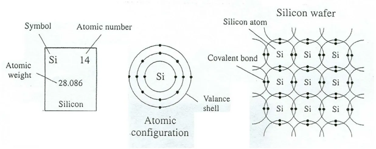
Are made by introducing different atoms, called dopant atoms, into the crystal. In pure form, Si wafer does not contain any free charge carriers.
Figure I-1: Crystal of pure silicon atoms
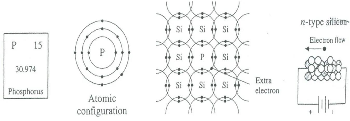
4 I-2-B-1-n-type: The dopant atoms added to the semiconductor crystal are donor atoms as P
atom ho has 5 electrons in their outermost shell of the column V of the periodic table [6] . For example, in the time when phosphorus impurity is added to Si, every phosphorus
atom’s four valence electrons are made up in a covalent bond with valence electrons of four neighboring Si atoms. However, the 5th valence electron of the phosphorus atom does not find a binding electron and thus remains free to float. When a voltage is applied across the silicon-phosphorus mixture, free electrons migrate toward the positive voltage end.
When phosphorus is added to Si to yield the above effect, we say that Si is doped with phosphorus. The resulting mixture is called N-type silicon (N: negative charge carrier silicon) [8].
Figure I-2: structure of silicon doped by phosphorous atom having N-type semiconductor
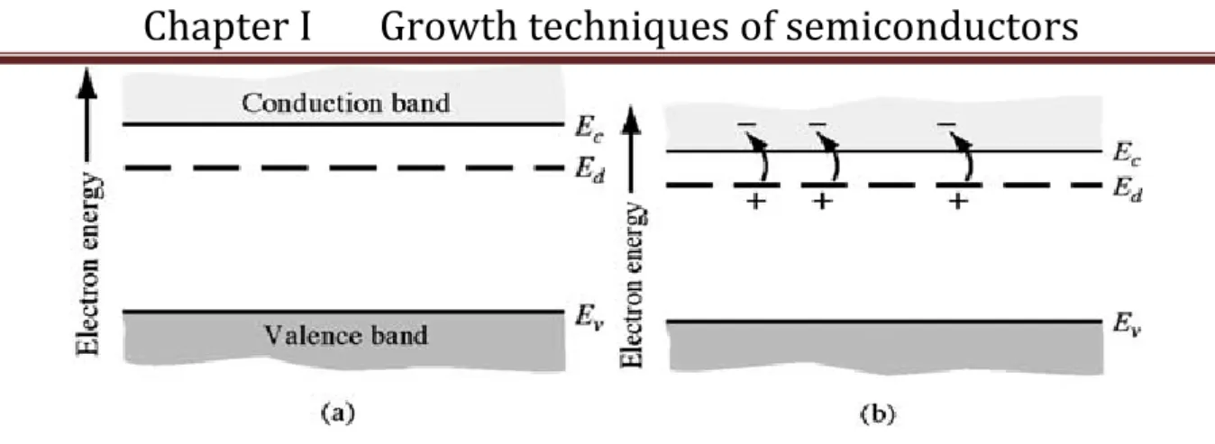
This type of impurity donates an electron to CB and so is called donor impurity atoms, which add electrons to contribute the CB current, without creating holes in VB.
The energy state of donor impurity defined by the energy level Ed
If a small quantity of energy, for example, thermal energy is added to the donor electron, it can be elevated into the CB, leaving behind a positively charged P ion [7].
Chapter I Growth techniques of semiconductors
5 Figure I-3: donor ionization energy levels.
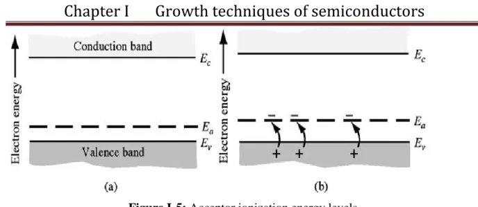
I-2-B-2: p-type semiconductor
In this type, a group III element, like B atom is added. 3 valence electrons are all taken up in covalent bonding; one covalent bonding position appears to be empty. The empty positions in the VB are thought of as holes.
The elements of group III atom accepts an electron from the VB and so is referred to as an acceptor [7].
FigureI-4: structure of silicon doped by boron atom having P-type semiconductor
The hole of Boron atom points goes to the negative terminal.
• The electron of neighboring silicon atom points passes to the positive terminal.
• The electron from neighboring silicon atom falls into the boron atom filling the hole in boron atom and creating a “new” hole in the silicon atom.
6 Figure I-5: Acceptor ionization energy levels
I-3-Growth Techniques
The historical starting point for virtually all semiconductor devices has been on the synthesis of single crystals. Today, three major methods have been developed to realize large-volume semiconductor crystals under thermodynamic equilibrium conditions: the Czochralski, Bridgman, and float-zone methods, which are discussed in the following subsections.
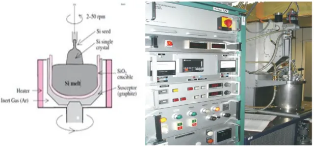
I-3-A-Czochralski Method
The Czochralski (CZ) crystal growth method was developed in 1916 by accident. Jan Czochralski, an engineer at the AEG Company in Berlin at that time, accidentally dipped his pen into a crucible containing molten tin and withdrew it quickly.
He observed a thin wire of solidified metal hanging at the tip. This small observation later led to the development of the Czochralski method for obtaining single crystals. [9]. The idea of this method was based on pulling of fibers of different metals from their melts. The obtained in such way metallic wires proved to be single crystals. The results of the experiments Czochralski published in Zeitschrift für Physikalische Chemie in 1918. This new technique allowed him to obtain the best quality single crystals of pure metals like Sn, Pb, Zn has grown in air later this method was adopted for crystal growth of semiconductors and oxides for electronic application.
Moreover, a modified Czochralski method allowed to obtain the single crystal of the intermetallic compounds, containing components even very reactive, sensitive to oxygen and other contamination. After separation of the growing crystal from the air, by use of growth chamber, an application of the protective atmosphere of inert gas e.g. Argon was possible. The application of the chamber additionally allows to heat starting materials under dynamic vacuum to remove adsorbed gases and additionally to control the gas pressure during the growth process. The next source of a possible contamination of the crystal is a contact of the melt with material of crucible. To eliminate this problem a water cooled cold crucible or
Chapter I Growth techniques of semiconductors
7
levitating coil, divided into segments with a proper profile, can be used. The levitation of ingot additionally allows to avoid the transport of the heat from the melt to the crucible and thus melting the materials even with high melting point. For investigation of the compounds containing the expensive noble elements a reduction of the cost of starting materials is available by the decrease of the ingot mass. However, there is a limitation of the Czochralski method to the growth from an ingot which melt congruent [10] [11] .
Figure I-6: Schematic setup for Czochralski process Figure I-7: Growth equipment
Figure I-8: AlSb single crystal obtained by CZ process
Advantages and disadvantages of Czochralski method
The Czochralski method possesses the several features as:
Extraction of the crystal in the opposite direction to the gravitation.
Crystallized materials are withdrawn from an ingot which melts congruently (without decomposition into the different phases). However, if the separation between the temperature of liquid and peritects line is narrow in the phase diagram, crystallization of the required compound is observed.
8
Spontaneous nucleation or by use of the oriented nucleus. The Czochralski immersed capillary in the melt for spontaneous nucleation of a single crystal. However, the spontaneous nucleation is also possible by necking of the withdrawn crystal in order to isolate single grain. This grain would expand into single crystal during the growth process;
Free growth, without tension caused by the limitations of the crucible; The possibility of applying the protective atmosphere;
Two disadvantages of the method belong
Tensions during the cooling down, necessity of warming up of the grown crystal, especially large;
Possible segregation of the constituents [10].
I-3-B-Bridgman Method
The Bridgman method based for a seed crystal is usually kept in contact with a melt, as in the Czochralski method. However, a temperature gradient is created along the length of the crucible so that the temperature around the seed crystal is below the melting point.
The crucible can be positioned either horizontally or vertically to control convection flow. As the seed crystal grows, the temperature profile is translated along the crucible by controlling the heaters along the furnace or by slowly moving the ampoule containing the seed crystal within the furnace [10] .
Figure I-9: Schematic setup for the Figure I-10: Growth equipment
Chapter I Growth techniques of semiconductors
9 I-3-C-The float zone method
Unlike the previous two methods, the float-zone (FZ) technique proceeds directly from a rod of polycrystalline material obtained from the purification process. The float Zone (FZ) method is based on the zone-melting principle and was invented by There in 1962. A schematic setup of the process is shown in (Fig I-11) the production takes place under vacuum or in an inert gas atmosphere. The process starts with a high-purity polycrystalline rod and a monocrystalline seed crystal that are held face to face in a vertical position and are rotated [9].
Figure I- 11: Schematic setup of the Float Zone (FZ) process.
With a radio frequency field, both are partially melted. The seed is brought up from below to make contact with the drop of melt formed at the tip of the poly rod. A necking process is carried out to establish a dislocation free crystal before the neck is allowed to increase in diameter to form a taper and reach the desired diameter for steady-state growth. As the molten zone is moved along the polysilicon rod, the molten silicon solidifies into a single Crystal and, simultaneously, the material is purified. Typical oxygen and carbon concentrations in FZ silicon are below 5 1015 cm-3. FZ crystals are doped by adding the
doping gas Phosphine (PH3) or di-Borane (B2H6) to the inert gas for n- and p-type,
respectively. Unlike CZ growth, the silicon molten Zone is not in contact with any substances except ambient gas, which may only contain doping gas. Therefore FZ silicon can easily achieve much higher purity and higher resistivity [9].
10 I-4. Conclusion
In this chapter, we discuss the most three famous techniques of crystal growth: the Czochralski, Bridgman, and float-zone methods; those used habitually in the industrial sector and we cited the different advantages of each technique.
CHAPTER II: Basic
Theory Of
11
II-I-Introduction
If the transverse electric fields increase in a solid material when it carries an electric current and is situated in a magnetic field that is perpendicular to the current. The electric field (Hall field), is a product of the force that the magnetic field exerts on the affecting positive or negative particles that create the electric current. Whether the current is a movement of positive particles, negative particles in the opposed direction, or a combination of the two, a perpendicular magnetic field displaces the affecting electric charges in the same direction to one side at right angles to both the magnetic field and the direction of current flow. The accumulation of charge on one side of the conductor leaves the other side oppositely charged and produces a difference of potential. A suitable meter (chapter 3) may detect this difference as a positive or negative voltage. The sign of this Hall voltage determines whether positive or negative charges are carrying the current.
In metals, the Hall voltages are usually negative, signifying that the electric current is collected by moving negative charges, or electrons. The Hall voltage is positive, on the other hand, for a little metal such as beryllium, zinc, and cadmium, indicating that these metals conduct electric currents by the movement of positively charged carriers called holes.
In semiconductors, in which the current consists of a movement of positive holes in one direction and electrons in the opposite direction, the sign of the Hall voltage shows which type of charge carrier is majorities. The Hall effect can be used also to measure the density of current carriers, their free will of movement, or mobility, as well as to detect the presence of a current in a magnetic field.
The Hall voltage that develops across a conductor is directly proportional to the current, to the magnetic field, and to the nature of the particular conducting material itself; the Hall voltage is inversely proportional to the thickness of the material in the direction of the magnetic field. Because various materials have different Hall coefficients, they develop different Hall voltages under the same conditions of size, electric current, and magnetic field. Hall coefficients may be determined experimentally and may vary with temperature.
Chapter II Basic theory of semiconductors
12
II-II -Energy band theory
II-II-1-Energy band model
If we will speak of the concept of the band energy, our understandings of the quantum mechanics will be the most useful model involves the concept of energy bands. Recall that electrons in an atom occupy discrete energy levels as shown in( Fig II- 1–a).
If two atoms are in close nearness, each energy level will divide into two due to the Pauli exclusion principle that states that each quantum state can be Occupied by no more than one electron in an electronic system such as an atom molecule, or crystal. When many atoms are brought into close proximity as in a crystal, the discrete energy levels are replaced with bands of energy states separated by gaps between the bands as shown in (Fig II- 1–b). One may think of an energy band as a semi continuum of a very large number of energy states.
Naturally, the electrons tend to fill up the small energy bands first. The lower the energy, the more totally a band is full. In a semiconductor, the majority of the energy bands will be basically totally filled (at absolute zero), while the high energy bands are basically totally empty. Between the (basically) totally filled and totally empty bands lie two bands that are only nearly filled and nearly empty as shown in (Fig II- 1–b).
The top nearly filled band is called the valence band and the lowest nearly empty band is called the conduction band.
The level between them is called the band gap. The electrons in a totally filled band do not have a net velocity and do not conduct current, just as the water in a totally filled bottle does not slosh about. Similarly, a totally empty band cannot contribute to current conduction. These are the reasons the valence band and the conduction band are the only energy bands that contribute to current flows in a semiconductor.
Figure II-1: the discrete energy states of atom (a) are replaced by the energy bands in crystal
13 II-II-2-The free electron model
The behavior of an electron in a crystalline solid is determined by studying the suitable Schrodinger equation. We study that this electron doesn’t in interaction with every one of the crystal, it may be written as:
2 2 ( ) ( ) ( ) 2m v r r E r (2-1) Where
V (r) is the crystal potential "seen" by the electron, (r) are the state function
E energy of this electron.
After resolution of eq (2-1) we get the solution
1 2
( )r c exp(ikx) c exp( ikx)
(2-2) Where 0 2 2m E k (2-3) When K represents the vector of the reciprocal space her unit is 𝒎−𝟏
We can get the value of the energy from the expression of K we have:
2 2 2 k E m (2-4)
According the equation (2-4), we will say that the energy of free electron has a discontinue value, but in reality, it’s not free in crystal it’s in interaction with nearly potentials of others electron in the lattice, then we pass to study the model with a periodic potential.
II-II-3-Periodic potentials
In most crystals, the interaction with the nuclei, or lattice atoms, is not negligible. However, the lattice has sure symmetries that the energy structure must also possess. The most important is periodicity, which is represented in the potential that will be seen by a
Chapter II Basic theory of semiconductors
14
nearly-free electron. Suppose we consider a one-dimensional crystal, which will suffice to illustrate the point, then for any vector L, which is a vector of the lattice, we will have:
V (x+l) =v (x)
Figure II-2: A: periodic potential in a one-dimensional crystal, B: The Kronig–Penney model
for a 1-D periodic lattice [13].
When we say that L is a vector of the lattice, this means that it may be written as L = na, Where n is an integer and a is the spacing of the atoms in the lattice. Thus, L can take only some values and is not a continuous variable. L then represents the periodicity of the lattice. The essential dot is that this periodicity must be imposed upon the wave functions arising from the Schrödinger equation, in this case with doing our study to two regions according the value of the potential, the first where v=0, and the second where V=V0
2 2 2 0 ( ) ( ) ( ) ( ) 2 x V x x E x m x (2-5)
We start the resolution in the first region v=0
The Schrödinger equation will be written as
2 2 2 0 ( ) ( ) 2 x E x m x (2-6) It means 2 0 2 2 2 ( ) ( ) 0 m E x x x
(2-7)15
The solution of this secondary equation is
( ) i x i x I x Ae Be (2-8) Where 0 2 2m E (2-9)
In the second region: V=V0, the Schrodinger equation rewrites as:
2 2 0 2 0 ( ) ( ) ( ) ( ) ( ) 2 x V x x E x x m x
(2-10) We rearranged (2-10)
2 2 0 2 0 ( ) ( ) ( ) ( ) 0 2 x V x E x x m x
(2-11)
2 0 0 2 2 2 ( ) ( ) ( ) ( ) 0 m x V x E x x x
(2-12)The solution of this secondary equation is
( ) x x II x Ce De (2-13) Where 0 2 2m V( E) (2-14)
If the wave function satisfies the Bloch theorem; it means Ψ is a periodic function, we can rewrite as:
( )x Uk( )x eikx
(2-15)
Where UK(x) is a periodic function with period x+L; and
( ) ( )
k k
U xL U x (2-16)
Chapter II Basic theory of semiconductors
16 ( ) ( ) ( ) i x L I x I x e (2-17) And in the second region( ) ( ) ( ) i x L II x II x e (2-18) Now we will set on these equations to get values to the constants A, B, C, and D
For that we established the conditions of continuities at x=0 and x= a with the first derivation at this point 1-Ψ (x) is continuous it must be I(0) II(0) at x=0 We get A+B=C+D (2-19) And ( ) ( ) I a II a At x=a
We used the Bloch theorem we get
exp(ik a( b)) Aexp(i b )Bexp(i b ) Cexp(a)Dexp(a) (2-20)
2- The continuity of derivation at x=0 and x=a means
( ) ( ) I II d x d x dx dx (2-21) At x=0 we have ( ) ( ) i A B CD (2-22) In x=a
exp(ik a( b i)) Aexp(i b )Bexp(i b ) Cexp(a)Dexp(a) (2-23)
The solution of this system of equations with four unknowns is represented as4×4 matrix form with determinant will be equal 0
0
1 1 1 1
0 0 exp( ( )) exp( ) exp( ( )) exp( ) exp( ) exp( )
0 exp( ( )) exp( ) exp( ( )) exp( ) exp( ) exp( )
A B i i C ik a b i b ik a b i b a a D ik a b i i b ik a b i i b a a (2-24)
17
The solution of this determinant with A, B, C and D not equal zero donated in this formulate (2-25) The first member of this equation depends only on E, through a and b are constants, so we can therefore be written as P (E). gets so
) cos
(E k( )
P a b (2-26) The figure II-3 shows P (E). By the Bloch theorem, k must be real. As a result, there is no possible solution to (2-26) for 1 P E ( ) 1 .This condition defines permissible energy ranges, hatched in (Figure II-3), called permissible energy bands, separated by ranges of forbidden energies, called band of forbidden energy.
Figure II-3: Graphical solution of the compatibility equation (P/qa) sin qa + cos qa = cos ka of the Kroning-Penney model.
Figure II-4: representation of the bands energies
2 2
sinh( ) sin( ) cosh( ) cos( ) cos( ( ))
2 a b a b k a b
Chapter II Basic theory of semiconductors
18
We can also obtain from Equation (2-25), the energy of an electron depending on k. This calculation provides a diagram E (k) such that shown in (Figure II-5).
Figure II-5: the energy as function of k
Given the periodicity of the crystal lattice, whose period is equal to a + b, and that of the reciprocal lattice, in the space of k, of periodicity 2
a b
; extend the curve of E (k)
from -∞ to +∞ with a period 2
a b
which gives the permissible energies according to k for all
the crystal dimensional [14].
Figure II-6: Energy as a function of k, repeated with 2
a b
. The first zone of Brillouin (ZB)
19
Applying the Born-von Karman boundary conditions for the expression of k for the one-dimensional crystal yields the values for k:
2 exp( ( ) 1 ( ) n ikN a b k N a b (2-27) Where
N, the number of atoms in the case of a one-dimensional crystal
The length of the crystal is equal to N (a+b). Since we limit our study of the first Brillouin zone, the k values which have to be considered are given by the following relationship.
k
a b a b
[14].
II-II-4-The Effective Mass Concept
The concept of effective mass is extremely helpful, in that it a lot enables us to treat the Bloch electron in an approach analogous to a free electron. Nonetheless, the Bloch electron exhibits many extraordinary properties which are unknown to those of a free electron [15].
We can define the group velocity as the velocity of the wave function of the electrons (analogous to the speed of sinusoidal wave) this can be written as:
( . )
( , )
( )
i k r t kr t
U r e
k
(2-28)Since the wave function for a Bloch-type wave packet extends over the entire crystal lattice, the group velocity for such a wave packet is given by
1 g d dE dk dk (2-29)
The group velocity of an electron wave packet is in the direction perpendicular to the constant-energy surface at a given wave vector k in k-space. It’s can be determined by the gradient of energy with respect to the wave vector k.
If a Lorentz force F, which may be due to either an electric field or a magnetic Field, applies to the electrons in a crystal, then the wave vector of electrons will change with the applied Lorentz force, according to the following relation:
(
g)
dk
F
q
B
dt
(2-30) WhereChapter II Basic theory of semiconductors
20
E is the electric field.
B is the magnetic flux density. The product dk
dt
is referred to as the change of crystal momentum. Equation (2-30) shows
that the external applied force acting on an electron tends to change the crystal momentum or the electron wave vector in a crystal lattice. The electron effective mass in a crystal lattice can be defined by g d F m a m dt
(2-31) [15]Replaced F and a by his value:
* F dk d 1 dE m dt dt a dt (2-32)
And the final expression of effective mass is:
1 2 * 2 2 d E m dk (2-33) II-II-4-1-Effective Mass Tensor
In three dimensional crystals the electron acceleration will not be collinear. Thus, in general we have an effective mass tensor.
1 1 1 g xx x yx x zx x d m F x m F y m F z dt (2-34) 1 1 1 1 1 1 * 1 1 1 1 xx xy xz yx yy yz zx zy zz m m m m m m m m m m (2-35)
The crystal and therefore the k-space can be aligned to the principal axis of the system centered at a band extrema. Since EK relationship is parabolic at that point, all off-diagonal
terms in the tensor will disappear [16].
21 Figure II-7: parabolic approximation for E-k diagram in the conduction band
If we are in the conduction band the values of energy written as
2 2 * 2 k c e k E E m (2-36) In this case the effective mass is in the lowest band, they have a positive sign
Figure II-8: parabolic approximation for E-k diagram in the valence band.
In the second time, the values of energy ware little to that of the valence band, it’s can written as: 2 2 * 2 k v h k E E m (2-37) We observed that E,k,ħ is a positive constant, and the values of Ek diminuate, it means that
Chapter II Basic theory of semiconductors
22
II-III-Equilibrium Properties of Semiconductors
II-III-1-Carrier Concentration and Fermi Level
We first consider the intrinsic case without impurities added to the semiconductor. The number of electrons (occupied conduction-band levels) is given by the total number of states N(E) multiplied by the occupancy F(E), integrated over the conduction band,
( ) ( )
c
E
n
N E F E dE (2-38) The density of states N (E) can be approximated by the density near the bottom of the conduction band for low-enough carrier densities and temperature:(2-39) Mc, is the number of equivalent minima in the conduction band
Mde* is the density of-state effective mass of electrons [18].
General expressions for the equilibrium densities of electrons and holes in a semiconductor can be derived using the Fermi–Dirac (F-D) distribution function and the density-of-states function. For undoped and lightly doped Semiconductors, the Maxwell– Boltzmann (M-B) distribution function is used instead of the F-D distribution function. If one assumes that the constant-energy surfaces near the bottom of the conduction band and the top of the valence band are spherical, then the equilibrium distribution functions for electrons in the conduction band and holes in the valence band may be described in terms of the F-D distribution function[19] .
The F-D distribution function for electrons in the conduction band is given by:
( )/
1
(
)
1
f B n E E K Tf
E
e
(2-40)Now to evaluate the integral (2-36)
(2-41) We make a change of variables y= (E-EC)/KBT we get:
3 * 2 2 3 0 ( ) 1 (2 ) exp exp( ) 2 F e E E n m KT y y dy KT
(2-42)After resolution, the result is
3 * 2 2 3 ( ) ( ) 1 (2 ) exp exp 2 2 C F C F e C E E E E n m KT N KT KT (2-43)
1 3 2 * 2 2 3 ( 1 (2 ) exp 2 C F e E C E E n m E E dE KT
3 1 * 2 2 2 3 ( ) 2 ( ) de C c m E E N E M 23 With: 3 * 2 2 2 2 e C m KT N (2-44)
Nc: called the "effective density of states in the conduction band"[13][18].
Figure II-9: graphic representation of density of state for a semiconductor type-n.
And the F-D distribution function for holes in the valence band can be expressed by:
( )/
1
(
)
1
f B n E E K Tf
E
e
(2-45)Doing the same work as in the case of distribution for electron, we get:
( ) exp F v v E E p N KT (2-46) With: 3 * 2 2 2 2 h v m KT N (2-47)
Chapter II Basic theory of semiconductors
24 Figure II-10: graphic representation of density of state for a semiconductor type-p.
II-III-2-Mass action law
2 i npn (2-48) ( ) ( ) exp c F exp F v c v E E E E np N N KT KT ( ) exp v c exp g c v c v E E E np N N N N KT KT (2-49)
This is true in general for non-degenerate semiconductors. For the case of intrinsic semiconductors we have the added constraint that ni pi so that
exp 2 g i i i i c v E n p n p N N KT (2-50) Or 3 2 3 * * 4 2 2 ( ) exp 2 2 B g i i e h K T E n p m m KT (2-51)
The expression of energy of Fermi level is obtained from equations (2-43) and (2-46)
( ) exp C F C E E n N KT ; ( ) exp F v v E E p N KT
25 1 1 ( ) ln 2 2 v Fi c v c N E E E KT N (2-52) * * 1 3 ( ) ln 2 4 h Fi c v e m E E E KT m (2-53) We have: 1 ( ) 2 midgap c v E E E * * 3 ln 4 h Fi midgap e m E E KT m (2-54)
According the equation (2-54) we conclude that in intrinsic semiconductor, the Fermi level is not exactly at the center between conduction and valence bands.
II-III-3-Ionization of impurity atoms in the extrinsic semiconductors
Let us consider,
n : thermal-equilibrium concentration of electrons p : thermal-equilibrium concentration of holes
nd : concentration of electrons in the donor energy state Pa : concentration of holes in the acceptor energy state Nd : concentration of donor atoms
Na : concentration of acceptor atoms
Nd+: concentration of positively charged donors (ionized donors)
Na- : concentration of negatively charged acceptors (ionized acceptors)
By definition,
d d d
N N n (2-55)
a a a
N N p (2-56) By the charge neutrality condition,
0 a d 0
n NN p (2-57)
0 ( a a) 0 ( d d)
n N p p N n (2-58) Assume complete ionisation,
Chapter II Basic theory of semiconductors
26 0 d a n p Then, eq (2-58) becomes, a d n N p NArranged the equation:
d a
np N N (2-59)
At the room temperature:
a a
N N ; Nd Nd
By eq (2-59) and the Mass-Action law we get:
2
2 4 p n p n pn (2-60)
2
2 2 4 d a i p n N N n
2 2 4 d a i pn N N n (2-61) Where (2-59)+ (2-61) we get:
2 2 1 4 2 d a d a i n N N N N n (2-62) (2-61) - (2-59) we get:
2 2 1 4 2 a d d a i P N N N N n (2-63)Using Relationships (2-61) and (2-48); for an N-type semiconductor, Nd Na and Nd ni
The electron and hole concentrations are given by:
2 d i d n N n p N (2-64)
In the case of semiconductor type p, the concentration of electron and hole we have a condition of Na NdandNa ni, so:
27 2 a i a p N n n N (2-65)
II-III-4-Position of Fermi level
Sc type N: We have exp ( C d) d C E E n N N KT
Doing the logarithm of this expression we get: ln c c F d N E E KT N (2-66)
Similarly for a p-doped material it is easily shown by combining equations (2-46) and (2-65)that ln F v v a N E E KT N (2-67)
Figure II-11: Position of Fermi level for an (a) n-type and (b) p-type semiconductor
It is seen that for high donor concentrations, the difference (EcEF) is reduced, hence the Fermi level will move closer to the bottom of the conduction band. Similarly, a high acceptor concentration will move the Fermi level closer to the valence band. This means that for extrinsic semiconductors, the Fermi level is different from the intrinsic Fermi level, i.e.
F i
E E [20].
Chapter II Basic theory of semiconductors
28
Any motion of free carriers in a semiconductor leads to a current. This motion can be caused by an electric field due to an externally applied voltage, since the carriers are charged particles. We will refer to this transport mechanism as carrier drift. In addition, carriers also move from regions where the carrier density is high to regions where the carrier density is low. This carrier transport mechanism is due to the thermal energy and the associated random motion of the carriers. We will refer to this transport mechanism as carrier diffusion. The total current in a semiconductor equals the sum of the drift and the diffusion current.
As one applies an electric field to a semiconductor, the electrostatic force causes the carriers to first accelerate and then reach a constant average velocity, v, due to collisions with impurities and lattice vibrations. The ratio of the velocity to the applied field is called the mobility. The velocity saturates at high electric fields reaching the saturation velocity. Additional scattering occurs when carriers flow at the surface of a semiconductor, resulting in a lower mobility due to surface or interface scattering mechanisms.
Diffusion of carriers is obtained by creating a carrier density gradient. Such gradient can be obtained by varying the doping density in a semiconductor or by applying a thermal gradient. Both carrier transport mechanisms are related since the same particles and scattering mechanisms are involved. This leads to a relationship between the mobility and the diffusion constant called the Einstein relation.
29
Assuming that all the carriers in the semiconductor move with the same average velocity, the current can be expressed as the total charge in the semiconductor divided by the time needed to travel from one electrode to the other, [20]or:
/ r Q Q I t L v (2-68) Where tr is the transit time of a particle, traveling with velocity, v, over the distance L.
The current density, J, can then be rewritten as a function of the charge density :
I Q J v v A AL (2-69) If the carriers are negatively charged electrons, (sc type N) the current density equals:
J en v
(2-70) And for sc type p the current density is:
J en v
(2-71)
It should be celebrated that carriers do not follow a straight path beside the electric field lines. in its place they bounce around in the semiconductor and constantly change direction and velocity due to scattering. This action occurs even when no electric field is applied and is due to the thermal energy of the carriers. Thermodynamics teaches us that electrons in a non-degenerate and non-relativistic electron gas have a thermal energy of kT/2 per particle per degree of freedom. A typical thermal velocity at room temperature is around 107 cm/s, which
exceeds the typical drift velocity in semiconductors. The carrier motion in the semiconductor in the absence and in the presence of an electric field can therefore be visualized as in (Figure II-13)
Chapter II Basic theory of semiconductors
30 Figure II-13:Random motion of carriers in semiconductors with and without
an applied electric field
1 ( ) n dn n t dt (2-72) 0 t t n dn dt n
0) 0 ( ( ) ( ) exp n t t n t n t (2-73)Amid all the electrons in the conduction band there are n t( )0 electrons which, at the instant
0
tt undergo a collision event. Let us follow the evolution of this electron population. At
0
tt some of these electrons will already have undergone new collisions. Therefore, at tt0
there is a smaller number of electrons, n(t), which have not yet undergone a collision result. The population of these electrons, n(t), decreases between t and t+dt by an amount dn according to the following equation:
In the absence of an applied electric field; we now analyze the carrier motion considering only the average velocity, of the carriers. Applying Newton's law, we state that the acceleration of the carriers is proportional to the applied force:
*dv F ma m e dt (2-74) 0 * 0 1 ( ) ( ) ( ) v t v t e t t m (2-75) If the collision is isotropic
0 * 1 ( ) ( ) v t e t t m
In the case of application of electric field, the expression of velocity will rewrite as:
0 ( ) 0 * ( ) 0 ( ) ( ) ( ) n t n t e v t t dn n t m
31 0 0 0 0 * 0 ( ) ( ) ( ) exp ( ) t t n n n t t t e v t t dt n t m
After evaluating the integral the final expression is:
* n n e v µ m (2-76)
Where µn is the mobility of a particle in the conduction band in a semiconductor, it’s large if
its mass is small and the time between scattering events is large.
Then we can describe the drift current as a function of the mobility, yielding: for electron n n J enµ (2-77-a) For holes p p J epµ (2-77-b) Where n p J J J ( ) n p n p J enµ epµ e nµ pµ (2-78) We can write also
J
Where
Represent the conductivity of material and( n p)
e nµ pµ
(2-79)
In the other time we can defined the resistivity of the material as the inverse of the conductivity [21]. 1 1 ( n p) e nµ pµ (2-80)
II-IV-1-The Hall Effect
The Hall effect is used in common practice to measure certain properties of semiconductors: explicitly, the carrier concentration (even down to a low level of 1012~ m -3),
Chapter II Basic theory of semiconductors
32
the mobility, and the type (n or p). It is a key analytical instrument since a simple conductance measurement [18].
The hall effect is a phenomenon that occurs in a semiconductor carrying a current when it is located in a magnetic field perpendicular to the current .the charge carriers in the semiconductor become deflected by the magnetic field and give rise to an electric field (Hall field)that is perpendicular to together the current and magnetic field .if the current density Jx
is along x and the magnetic field Bz along z then the hall field is also along +y or –y
depending on the polarity of the charge carriers in the material[21].
Figure II-14: Hall Effect geometry in sc type n and sc type p
We may calculate the Hall field in the following manner. The Lorentz force acting on an electron is: ( ) 0 Fq E v B (2-81) This becomes: y x z qE qv B We can write: H H V E W Where x
v is the drift velocity vx J ne
33
Where n is the number of charge carriers per unit volume.
H z H
J
E B R JB
ne
(2-82)
Where RH called Hall coefficient, and
1
H
R
ne
(2-83-a)
Generally for N-type material from the Hall field is developed in a negative direction compared to the field developed in a P-type material, a negative sign is used while denoting hall coefficient RH
For sc type p RH 1 pe
(2-83-b) For a semiconductor with significant concentrations of both types of carriers:
2 2 ( ) h e H H e h pµ nµ E R JB e nµ pµ (2-84) II-IV-1-1_Hall Effect and Mobility:
When one carrier dominates, we can write the conductivity:
We have: neµefor electrons or peµp(for holes)
So the mobility can be written:
/ H /
µ R (2-85)
II-IV-1-2-Diffusion current
In semiconductors, current can be created due to a concentration gradient of carriers. The current in this case is called diffusion current and is derived below. Consider a piece of semiconductor in which, for whatever cause, there is an electron concentration gradient. By analogy with the laws of diffusion in gases or liquids one can simply imagine that electrons will diffuse from the region where their concentration is highest in the region where it is lowest. The flux of electrons, Fn resulting from the diffusion process is directly proportional to the electron concentration gradient, dn
dx . This flux, when multiplied by -q, is
equal to the diffusion current density of the electrons: [13]
In the absence of electric field, E=0
n n dn F D dx (2-86) Where n n n dn J qF D dx
Chapter II Basic theory of semiconductors
34
(2-87)
Similarly for holes we have:
p p dp F D dx (2-88) So: Jn qFn qDp dp dx (2-89) n
D And Dpare constants called "diffusion coefficients" for electrons and holes, respectively. They represent the ease or the "fluidity" with which the carriers can move and diffuse in the semiconductor material.
Figure II-15: carriers concentration gradient and the resulting diffusion currents. In the presence of electric field:
At 1D: (2-90-a) p p p dp J qµ p qD dx (2-90-b) At 3D: For electron: ( ) n n n J qµ nqD grad n (2-91-a) For holes: ( ) p p p J qµ pqD grad p (2-91-b) Where: n p J J J II-IV-1-3-Einstein relationships: n n n dn J qµ n qD dx
35
In the case when no electric field applied, J=0 For electron 0 n n n dn J qµ n qD dx Where dv dx
Replacing the value of energy in the equation, we get:
0 n n n dv dn J qµ n qD dx dx n n dv dn µ n D dx dx
Replacing n by her value:
0 exp( )
dn e ev ne
n
dv KT KT KT
The final expression of mobility is:
n n e µ D KT (2-92-a)
For holes same works and
(2-92-b)
II-V-conclusion
In the material semiconductor the displacement of charge carriers between the conduction and valence bands who is responsible for the conduction phenomenon, we can distinguish two types of charge carriers n and p and same one of them have a characteristic different from another.
To develop the conductivity of the material we used different technic as variation in concentration of dopant and the variation in temperature and the external applied forces as electric and magnetic fields
The Hall Effect is the best and useful technique to determine the type of charge carriers in the conductive material experimentally.
p p
e
µ D
KT
Chapter II Basic theory of semiconductors
36
The conductivity of material has a direct relationship with the concentration of dopant and the temperature.
Chapter III: Results
and Discussions
37
III-1-Objective of the experiment:
Determination of hall coefficient for Geranium doped p
Observation of the Hall Effect, and measurement of the Hall constant of a Ge type P semiconductor
III-2-Manipulation:
The following figure presents the materials that used in our laboratory. In fact, we can measure the Hall coefficient using two baths, first one is direct measure and the second bath is measured with the help of Cassy lab 2 program; we took the second bath.
Figure III-1: Materials of manipulation. Apparatus
1- DC Power Supply 2- PC with Windows 3&4- DC Power Supply 5- Leybold Multi clamp 6- Base unit for Hall effect
7- Extension cable, 15-pole blue and red
CHAPTER III RESULTS AND DISCUSSI ONS
38
8- P-doped Ge plug-in board (Figure 2)
Figure III- 2: P-doped germanium on plug-in board Technical characteristics
Crystal dimensions: 20mm x 10mm x 1mm
Multiple socket for connecting the printed circuit board to the base unit for studying the Hall effect Dimensions: 10 cm x 10 cm x 1 cm
Mass: 200 g.
After realization of montage (Figure III-1) and connect the fill we do the measurement, manual and we take the result.
III-3-Measuring the Hall voltage as a function of magnetic field:
In the first we make the experience with measurement of the Hall voltage as a function of the magnetic field in a constant value of current.
We retry our result with a different value of current I=10mA and I= 15mA.
For I=15mA: B / T UH / V 0,05 0,002 0,12 0,028 0,17 0,049 0,48 0,161
39 0,54 0,183 0,70 0,236 0,85 0,389 1,17 0,401 1,32 0,457 1,47 0,512 1,62 0,572 For I= 10mA B/T UH/V 0,05 0,00129 0,32 0,06 0,38 0,07355 0,55 0,1129 0,70 0,14645 1,02 0,21032 1,09 0,23097 1,27 0,27097 1,38 0,29806 1,53 0,33484 1,62 0,36065
After the measurement, we represent these values on the graph using the Origine8 program as following figure
Figure III-3 : Variation of UH(v) as a function of B(T). 0,00129 0,06 0 6 12 I=10A I=15 A UH (V) B(T)
CHAPTER III RESULTS AND DISCUSSI ONS
40 Interpretation of results:
Through the results obtained by the two programs; Cassy lab2 and origin8, we notice a match in the two axes, each of which is a straight line, equivalent to the form U (B) = K.
Where K is a constant current.
The term is consistent with the term obtained theoretically, regardless of current intensity So we conclude that we have proportionally between the hall voltage and the magnetic field passing is the circuit in a constant.
For the measurement with I =10A in the figure 3 the slope: . 2.9806 0.07355 0.22 / 1.38 0.38 H R B A V T d
The Hall coefficient RH is obtained as follows:
d =1⋅10-3m I =10 mA 3 2 0.22 10 2.2 / 10 H Ad R mV TA I
III-4-Measuring the Hall voltage as a function of current:
For the second step we make the experience with measurement of the Hall voltage as a function of the current at a constant value of magnetic field (B=0.2T, B=0.29T and B=0.37T) and room temperature. For these three different values we measure the UH=f(I) as the
following tables show.
For B=0.2T: I/A*10-3 U H/V*10-2 1.0 2.61 1.2 2.81 1.3 3.00 1.4 3.20 1.5 3.40 1.6 3.61
41 1.7 3.8 1.8 4.01 2.0 4.21 2.1 4.42 2.2 4.60 2.3 4.81 2.4 5.00 2.6 5.20 2.7 5.41 2.8 5.58 2.9 5.81 3.0 6.03 3.1 6.21 3.2 6.41 3.3 6.62 3.5 6.80 1.0 7.00 1.2 7.20 1.3 7.40 1.4 7.62 For B=0.29T: I/A*10-3 U H/V*10-2 1.2 3.21 1.3 3.41 1.5 3.61 1.6 3.79 1.8 4.01 1.93 4.20 2.08 4.398 2.23 4.596 2.38 4.794


![Figure II-1: the discrete energy states of atom (a) are replaced by the energy bands in crystal (b) [12]](https://thumb-eu.123doks.com/thumbv2/123doknet/13819590.442493/24.892.198.692.852.1041/figure-discrete-energy-states-replaced-energy-bands-crystal.webp)
![Figure II-2: A: periodic potential in a one-dimensional crystal, B: The Kronig–Penney model for a 1-D periodic lattice [13]](https://thumb-eu.123doks.com/thumbv2/123doknet/13819590.442493/26.892.132.762.225.466/figure-periodic-potential-dimensional-crystal-kronig-penney-periodic.webp)