.. , I '.
A 2.5 Gb/s SONET Clock and Data Recovery
Macro Cell
by
Andrew Holden Dickson
Submitted to the Department of Electrical Engineering and Computer Science in partial fulfillment of the requirements for the degrees of
Master of Science
and
Bachelor of Science
at the
MASSACHUSETTS INSTITUTE OF TECHNOLOGY
May 1994
( Andrew Holden Dickson, MCMXCIV. All rights reserved.
The author hereby grants to MIT permission to reproduce and distribute publicly paper and electronic copies of this thesis document in whole or in part, and to grant
others the right to do so.
Author . . . ...
Department of Electrical Engineering nA Computer Science May 18, 1994
Certified
by ...
...
Hae-Seung Lee Professor Certified by ... r Thesis Supervisor Douglas Hoy ManagerAccepted
by...
A 2.5 Gb/s SONET Clock and Data Recovery Macro Cell
by
Andrew Holden Dickson
Submitted to the Department of Electrical Engineering and Computer Science on May 18, 1994, in partial fulfillment of the
requirements for the degrees of Master of Science
and
Bachelor of Science
Abstract
This thesis covers the design and SPICE simulation of a 2.5 Gb/s clock and data re-covery integrated circuit suitable for a SONET OC-48 based system. Critical circuits, such as the VCO and the phase-detector were analyzed and simulated with SPICE in detail. The design is evaluated for compliance with the SONET standard specifica-tions of phase noise, jitter, etc. using a temperature range of 25 deg C to 125 deg C, a supply voltage of -5.2V ± 400mV, and ±3 sigma process limits (up/down model libraries). Extracted layout parasitic capacitors are included in the final simulations.
Device models for SPICE are taken from Tektronix Component Corporation GST-1, a high speed self-aligned double-polysilicon bipolar process with an ft > 12 GHz.
Thesis Supervisor: Hae-Seung Lee Title: Professor
Thesis Supervisor: Douglas Hoy Title: Manager
Acknowledgments
First of all I thank my parents who have been a blessing and a loving support to me throughout my entire education. Without their support and encouragement I would never have made it to or through MIT.
A large thank you to Doug Hoy, my manager at Tektronix, for giving me the op-portunity to work on a project like this. His knowledge and expertise of digital and system-level design were necessary to help me complete this project.
Much thanks goes to Chris Martinez for his analog design help, and fellow group members Cary Renzema and George Caspell for their support and circuit ideas.
I am indebted to Jim Lamb and Art Metz who gave up many hours to discuss circuit ideas, oscillator noise, and phase-locked loops. Skip Hillman, Linley Gumm, Larry
Contents
1 Introduction
1.1 General Description .
2 The SONET OC-48/SDH STM-16 2.1 SONET/SDH Basics ...
2.1.1 Signal Rates ...
2.1.2 Frames . ...
Standard
3 Phase-Locked Loop Basics 3.1 Definitions.
3.2 Phase-Locked Loops .... 3.3 Loop Filter Selection .... 3.4 PLL Tracking Performance .
4 Phase-Locked Loop Parameter Calculation 4.1 Pattern Dependence Test Constraints ....
4.2 Jitter Tolerance Constraints ...
4.3 Phase-Locked Loop Parameter Curves . . .
4.4 Jitter Transfer Constraints ...
5 Clock Recovery and Data Re-timing Circuit Design 5.1 Phase and Frequency Detection ...
5.2 Phase and Frequency Detector Design... 5.3 Signal Multiplexers. 11 12 17 18 18 18 21 21 22 25 29 31
... . .31
. . . .35 . . . .37 . . . .39 41 42 46 545.4 VCO Design ... 5.5 Active Filter Design.
5.6 Data Re-timing . . . . .
6 Signal Detect Circuit Design
7 Frame Detect and 1:16 Demux Design 7.1 Shift and Compare ... 7.2 1:16 Demultiplexer.
7.3 Control Block ...
8 Conclusion
8.1 Summary ... 8.2 Future Considerations.
8.2.1 Analog/Digital Phase Detector Trade-offs ...
A The Tektronix GST-1 Process, Modeling, and Standard Cells A.1 The GST-1 Process ...
A.2 The GST-1 Digital Standard Cell Library ...
B Applicable SONET/SDH Requirements B.1 SONET Requirements.
B.1.1 Loss Of Signal (LOS) ...
B.1.2 Pull-in/Hold-in ...
B.1.3 Jitter...
B.2 CCITT Requirements ...
B.2.1 STM-N Pattern Dependence Test
C Receiver I/O summary
C.1 Inputs...
C.2 Outputs ...
D Flip-latch and Latch-latch Logic
55 61 66 69 73 74 79 83 90 90 90 90 93 93 93 95 ... ...95 ... ...95 ... ...96 ... ...97 ... ...98 ... ...98 101 102 104 105
D.1 The Flip-Latch Concept ... 105
List of Figures
1-1 Block Diagram of an Add/Drop Multiplexer . . ... 13
1-2 Receiver Block Diagram . ... 14
2-1 SONET STS-1 Frame ... 19
2-2 Time-Division Multiplexing of SONET frames ... 20
3-1 Linear phase-locked loop model ... .. 22
3-2 Ideal VCO model and characteristic ... 22
3-3 Ideal phase detector model and characteristic ... 23
3-4 Passive and active filter models ... 26
3-5 Second-order PLL open- and closed-loop response . ... 28
3-6 Linear phase-locked loop model with VCO phase noise ... 29
4-1 Constant CCITT phase error curves in the -wn plane ... 34
4-2 Constant SONET phase error curves in the (-wn plane ... 36
4-3 Allowed parameter range to guarantee a phase error of less than 7 . . 37
4-4 Allowed parameter range to guarantee a phase error of less than 3 . . 38
5-1 Block Diagram of the clock recovery and data retiming system .... 42
5-2 Block Diagram of the FPLL ... . ... . 43
5-3 Timing diagram of the FPLL out of frequency lock ... 44
5-4 Timing diagram of the FPLL in frequency lock ... 45
5-5 Sample and hold phase detector ... .. 46
5-6 One half of a differential track and hold circuit ... 47
Modified track and hold circuit ...
Track-and-hold input buffer ...
Analog Multiplexer ...
Sample-and-hold phase detector characteristic ...
Frequency Detector ...
Ring VCO with in-phase and quadrature frequency-doubled outputs 5-14 Variable delay cell schematic
Variable delay cell in the up-state ... Variable delay cell in the down-state ...
Modified VCO control voltage generator . . . Simulated VCO tuning characteristic ... Basic circuit diagram for the charge pump . . Simplified charge pump circuit ...
Simplified charge pump with output resistance Simulated filter frequency response ... Timing diagram of data re-timing...
Block Diagram of the Signal Detect Block . . Delay-XOR circuit and timing diagram ....
Block Diagram of the Set/Reset Generator . .
7-1 Basic parallel frame detect diagram ....
7_) Q;trmn"liF.pl -ixrs L.- L, U LIIJ hit; UL t, okhf J.. rOjJ. ior .rolG . .t . .. . . . . . . .. Bit positions along the shift register at a given point in time
AND-latch/Mux-latch equivalent functionality ...
A 2-bit shift cell with 10 decoding logic ... The byte compare block ...
The final compare block ...
The parallel output circuitry attached to a 2-bit shift cell . .
STROBE timing diagram ... .
Control block reset logic ... .. 5-8 5-9 5-10 5-11 5-12 5-13 5-15 5-16 5-17 5-18 5-19 5-20 5-21 5-22 5-23 6-1 6-2 6-3 49 51 52 53 53 55 57 57 58 59 60 61 62 64 65 67 70 70 71 74 75 76 77 78 79 80 81 82 83 7-3 7-4 7-5 7-6 7-7 7-8 7-9 7-10 I -A
7-11 Control block select logic ... ... 84
7-12 Diagram of the DIV16 divider . ... 85
7-13 A 4-bit pseudo-random sequence generator and its sequence table . . 86
7-14 Circuit for the DIV8ST divider ... 87
7-15 Timing diagram for parallel output clock and data ... 88
7-16 Timing diagram for serial output clock and data ... 89
B-1 SONET Category II Jitter Transfer Characteristics ... 98
B-2 SONET Category II Jitter Tolerance Mask ... 99
B-3 CCITT pattern dependence test sequence ... 99
D-1 Basic flip-latch architecture . ... 105
D-2 Analog Sample and Hold Phase Detector ... 106
List of Tables
2.1 SONET/SDH Designated Signal Rates ... 18
Chapter 1
Introduction
The current generation and the next generation of fiber optic telecommunications is driving the clock and data speeds to multi-GHz rates. A set of standards, known as SONET (Synchronous Optical Network) or SDH (Synchronous Digital Hierarchy), has been developed in order to standardize global high-speed optical communication. The SONET OC-48 or SDH STM-16 standard is a multi-layer operations, administration, maintenance and provisioning standard, covering the path, section, line, and physical
layers of a communication system. The physical layer of these standards consists of an optical 2.48832 Gb/s NRZ scrambled serial data stream.
Because of the high clock rate of OC-48/STM-16, more of the required function-ality, such as byte alignment, frame detection and demultiplexing, are constrained to monolithic or hybrid package implementation. The move towards fully integrated clock and data recovery is also motivated by space requirements. Clock recovery at this speed requires high precision components in order to provide fast acquisition and at the same time, low phase noise. Many high frequency clock recovery units use Surface Acoustic Wave (SAW) filters which have very high Qs, but cannot be fully integrated using present technology. Complete OC-48/STM-16 rate Phase-Locked Loops (PLL) have be implemented on a single chip [2, 5], reducing cost, complexity, space, and power requirements. Few of these have been produced for the commercial market, and none have been further integrated to include significant digital processing
It is for these reasons, among others, that there is a need for a high-speed clock recovery IC with a higher level of integration. It is desirable that the data output of the IC be demultiplexed down to a low enough rate so that further processing can be accomplished with a lower-speed, lower-cost, highly integrated and less power-hungry CMOS IC. Power is also reduced due to lower-speed outputs, and the cost and sensitivity of the board level design is relaxed, such as routing and transmission line design.
This thesis covers the development of a OC-48/STM-16 rate clock and data recov-ery IC which meets these needs, providing integrated byte alignment, frame detection, and a 1:16 data demultiplexer. The macro cell is intended to be used on a larger chip that also contains a post-amplifier and all the necessary input and output (I/O) cells-the development of the post-amp and the I/O cells will not be covered in this thesis.
In order to attain this project goal, a high-performance bipolar process is used, along with accurate device modeling and simulation tools. The Tektronix GST-1 Si-bipolar process is ideal for this task, with an npn fT > 12 GHz and excellent device
modeling over a wide range of temperature and process variations. For the digital logic, the Tektronix GST-1 standard cell library provides the necessary resources for accurate modeling as well as functional testing. See Appenix A for additional information about the GST-1 process and modeling.
1.1 General Description
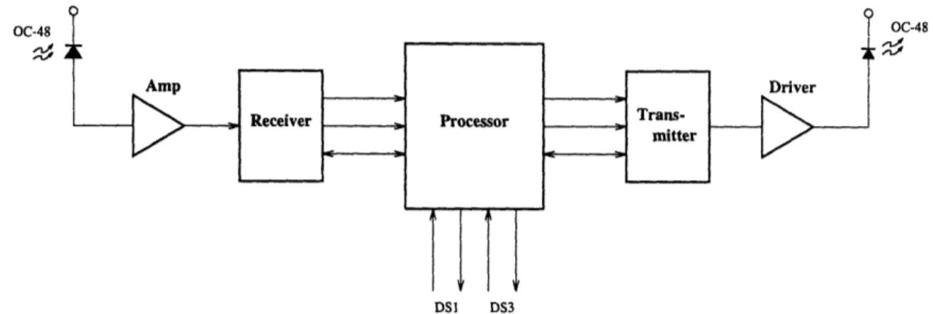
The IC that includes the macro cell covered in this thesis can be used in the re-ceiver front-end of a system such as an add/drop multiplexer (shown in Figure 1-1), regenerator, cross-connect, line terminator, or a variety of test equipment. On the system level, the IC lies directly after the optical-to-electrical conversion and the pre-amplifier, and right before the descrambling, overhead processing, and further de-multiplexing. The IC contains an on-chip frequency- and phase-locked loop (FPLL) to recover the clock and re-time the data from a 2.48832 Gb/s Non-Return-to-Zero
OC-48
DSI DS3
Figure 1-1: Block Diagram of an Add/Drop Multiplexer
(NRZ) serial data stream, and outputs the data in 16 parallel data lines each running
at 155.52 Mb/s. It also provides lock detect, byte alignment, frame detection, and supplies a steady output clock if the data signal has been lost. The SONET/SDH framing bytes are used to provide byte alignment and frame detection.
A block diagram of the receiver is shown in Figure 1-2. As stated previously, the design of the post amp and I/O cells will not be covered in this thesis, but will be integrated onto the final IC design. There are three separate input paths to the chip to give the system designer flexibility in designing and testing the chip. The main
data input to the chip under typical operating conditions is the Serial Data Input
(SDI) line which is intended to be driven by the optical-to-electrical converter pre-amplifier. This line is fed directly into a post-amplifier (post-amp) which regenerates the single-ended, small-signal input to a differential, digital-level signal. If an external
post-amp is used instead of the internal post-amp, the Bypass Serial Data Input
(BPSDI) lines serve to bypass the internal post-amp when the Bypass Post-Amp Enable (BPPAE) line is asserted high. Also, a Loopback Serial Data Input (LBSDI) is provided to facilitate in-system diagnostic loopback testing. This input is enabled when the Loopback Enable (LBE) line is asserted high. Both the BPSDI and LBSDI inputs are differential digital ECL inputs.
If the signal power on SDI should fall below a specified threshold, the post amp asserts the Loss-Of-Power Indicator (LOPI) line, signaling that the data is most likely invalid. This may happen in the case of a break in the fiber optic cable or a
LOPI BPPAE LBE SDI BPSDI LBSDI RCLKI LOSI FP PDO PCLKO SDOI SDO2 SCLKO CFI CF2 SOE
Figure 1-2: Receiver Block Diagram
transmitter failure-no valid data is present on the input lines, but noise inherent in the system may still cause transitions across the digital threshold levels. If the on-chip post-amp is bypassed (BPPAE high), the External Loss-Of-Power (ELOP) line must be attached to the off-chip post amp power sensing output.
The Signal Detect block is similar to the loss-of-power indicator in the post-amp in that it senses a Loss-Of-Signal (LOS) condition. The difference is that the Signal Detect block detects the loss of transitions in the data stream. This block is essentially a digital counter which is reset by any transition on the selected serial data input line. If no transitions occur within a certain number of bit periods, the Loss-Of-Signal Indicator (LOSI) line is asserted. If a loss-of-power condition exists (either LOPI or ELOP line asserted), the LOSI line is automatically asserted. When the Clock Recovery block is bypassed (see below) the Signal Detect block output is disabled.
The Clock Recovery block is a frequency- and phase-locked loop (FPLL) which extracts a synchronous clock signal from the selected serial data input. The FPLL consists of a voltage controlled oscillator (VCO), two phase detectors (PD), a fre-quency detector (FP), and a loop filter/amplifier with an off-chip capacitor. If a LOSI
condition should occur, the FPLL locks onto the reference clock input (RCLKI) to provide a steady output clock.
The Frame Detect/Demux block is a digital block which provides the necessary byte and frame alignment, as well as the 16-bit parallel output. The core of this block is a 24-bit shift register and pipelined decoding logic which searches the re-timed serial data for an A1A1A2 framing pattern (See Chapter 2). The Frame Pulse (FP) line is a synchronous periodic signal which indicates that a valid A1A1A2 framing pattern has been found and that the demultiplexer is in proper byte alignment. The FP line is asserted once per frame, one byte after an A1A1A2 sequence is found, and it is asserted for one two-byte period. The SYN line is a single-ended, active falling edge signal which allows the Frame Detect block to re-align with the incoming data. The demultiplexer uses a resettable clock divider to divide the extracted clock signal down
and latch 16 bits of data from the frame detect shift register with the proper byte
alignment. The 16 parallel data lines (PD00-PDO15) from the Demux block are at a 155.52 Mb/s data rate, and the associated clock (PCLKO) is a half-speed clock (77.76 MHz) which can be used to latch the data on each edge. The TESTEN line allows full functional testing of the Frame Detect/Demux block, even at full-speed if necessary. For this test, TESTEN is asserted high, the data signal should be applied to the RCLKI lines and the associated clock signal should be applied to the TCLKI
lines.
After lock has been acheived and an A1A1A2 sequence has been detected, the receiver will remain in byte alignment until a LOSI condition exists or the SYN line is asserted. In the case of an LOSI condition, the Clock Recovery and Frame Detect blocks are reset and the Demux output is disabled. If SYN is asserted, the Frame Detect block is reset and the Demux output is disabled, but the Clock recovery block will remain locked to the serial data stream.
The re-timed serial data and its associated clock are available as outputs when the Serial Output Enable (SOE) line is asserted. The data is brought out on two separate 1.24416 Gb/s serial streams (SDO1 and SD02). These data lines are clocked on each edge of the Serial Clock Output (SCLKO) line, the associated 1.24416 GHz clock.
These lines are intended to be connected to the transmitter to allow in-system line
loopback testing, but under normal operating conditions the outputs are squelched
to reduce on-chip noise.
Chapter 2 is an overview of the SONET/SDH basics, including a review of the necessary specifications for the receiver. Chapter 3 covers the basics of phase-locked loops (PLL) and some relevant performance issues. Chapter 4 begins the design of the receiver, containing the calculations for the necessary PLL parameters to achieve the specifications. Chapters 5, 6 and 7 cover the design of the clock recovery, signal detect, and frame detect/demux circuits respectively.
Chapter 2
The SONET OC-48/SDH STM-16
Standard
Different countries around the world have their own telephone standards which are not directy compatible with each other. Even within countries such as the United States there are various vendors with incompatible architectures, equipment, codes, etc. that make connection between carriers difficult. These and other problems are major obstacles between connecting systems from around the world together in a unified, global communication network.
The SONET concept was first proposed by Bellcore, recognized by the Amer-ican National Standards Institute (ANSI), and developed by the Exchange Carri-ers Standards Association (ECSA) and the International Telegraph and Telephone Consultative Committee (CCITT) in an effort to unify global telecommunications. SONET/SDH defines a set of standard interfaces, signal rates, synchronous mul-tiplexing formats, etc. The standards are designed to create a flexible, long-term
"future-proof" solution that allows multi-vendor networking, transmission of a wide variety of types and rates of data, and a host of other benefits. [1, 8, 9]
Electrical Signal STS-1 STS-3 STS-9 STS-12 STS-18 STS-24 STS-36 STS-48 Optical Signal OC-1 OC-3 OC-9 OC-12 OC-18 OC-24 OC-36 OC-48 Data Rate (Mb/s) 51.84 155.52 466.56 622.08 933.12 1244.16 1866.24 2488.32 CCITT Designation STM-0 STM-1 STM-4 STM-16
Table 2.1: SONET/SDH Designated Signal Rates
2.1
SONET/SDH Basics
2.1.1
Signal Rates
The basic SONET signal is called the Synchronous Transport Signal level-1, or STS-1, which is a 51.84 Mb/s serial data stream-the optical equivalent signal is known as Optical Channel or Optical Carrier level-i, abbreviated as OC-1. The CCITT standards designate signal rates in multiples of the Synchronous Transport
Module-1, or STM-Module-1, which is equivalent to three times the STS-1 rate. The SONET/SDH signals can be time-division multiplexed in specific byte-interleaved integer multiples of the basic rates. See Table 2.1 for a listing of the rate designations. A multiplexed N-integer multiple of a STS-1, OC-1, or STM-1 rate is generally referred to as STS-N, OC-N, or STM-N rate respectively.
2.1.2
Frames
Information is transmitted over the physical layer in "frames" of 9-byte row by 90-byte column matrices which are made up of the "payload" information and overhead bytes. The SONET STS-1 frame is shown in Figure 2-1. The bytes in each frame are transmitted row-by-row from top to bottom and from left to right. The first 3 columns of an STS-1 frame are Transport Overhead (TOH) bytes which contains
Transport Synchronous
Overhead Payload Envelope
Section Overhead Line Overhead Path Overhead
Figure 2-1: SONET STS-1 Frame
framing bytes and administrative information. The other 87 columns in the frame make up the Synchronous Payload Envelope (SPE). The SPE contains the main digital information such as telecommunication or video data, but the first column of the SPE is reserved for the path overhead. The SPE can take on many different formats depending on the type of data that it carries. Many types of data can be accepted-voice data such as telephone conversations, video data such as NTSC-quality or compressed HDTV, and other types of digital information such as computer data. Standard signals which can be transported include DS1, DS1C, DS2, DS3, CEPT-1, CEPT-4 and other types of Broadband ISDN, all of which can be packed into STS-1 or special STS-3c concatenated frames.
Every byte in the overhead section is labelled and has a certain function, some of which are reserved for future designation. The first three rows of the TOH is called the section overhead. It is used for frame synchronization, payload numbering, parity error monitoring, and message signals between equipment. The remaining six rows of the TOH is called the line overhead which is used for pointers, alarm indications, as well as parity error monitoring and message signals between equipment.
Frames can be multiplexed together to form higher-rate formats using a
byte-Al A2 Cl B1 El F1 D1 D2 D3 H1 H2 H3 B2 K1 K2 D4 D5 D6 D7 D8 D9 D10 D11 D12 Z1 Z2 E2 i i -B 3 -C 2 -G I -F 2 -H 4 -D -Z 4 - -Z 5
-STS- I a
Ala A2a Cla Jla .
STS-3 STS-lb
Ala Alb Alc A2a A2b A2c Ca Cb Clc Ja - Alb A2b Cb Jib -
--STS-lc
Aic A2c Clc Jlc
Figure 2-2: Time-Division Multiplexing of SONET frames
interleaved Time-Division Multiplexed (TDM) scheme. Figure 2-2 shows an example of this interleaving scheme for three input STS-1 streams.
Because of this multiplexing scheme, the first 2N bytes in any STS-N frame are always the Al and A2 framing bytes-NxAl bytes followed by NxA2 bytes. These bytes are used to synchronize the receiver to the incoming byte and frame boundaries. The Al, A2 and C1 (payload number) bytes are the only bytes that are not scrambled for transmission across the physical layer. A common technique is to use a frame detector which is designed to scan the serial data for the boundary between the Al
and A2 bytes.
Each STS-N/STM-N frame is a fixed 125/us in length. This frame time does not vary with the multiple number N. Take for example three STS-1 signals multiplexed up to an STS-3 rate-the frame contains three times more data but the signal rate is increased three fold, which gives the same frame time and effective throughput for each of the three STS-1 signals.
There are two specifications in the SONET/SDH standards which constrain the design and must be kept in mind, jitter tolerance and the pattern dependence test. Another specification, jitter transfer is not required because of the application, but we will see that it is useful in the design analysis. Appendix B has listing of these specifications.
Chapter 3
Phase-Locked Loop Basics
3.1 Definitions
Jitter can be thought of as the random phase variation on a waveform. In the context
of a digital clock or data pattern, it describes the movement of an edge from its ideal location in time. This can be due to various sources of noise. Jitter is sometimes defined separately from wander, which can be thought of as low-frequency jitter. It is usually desirable to track wander due to its large, slow phase variations.
Jitter tolerance, in the context of a phase-locked loop (PLL), describes the
max-imum amount of input jitter that the PLL can track without losing lock. This is usually a specifications which states the minimum amount of phase jitter that a PLL should be able to track at various frequencies.
Jitter transfer is used to describe the transfer characteristic of phase input to
phase output in a PLL. The maximum amount of jitter transferred from input to output is usually specified in order to reduce the total jitter in a system.
Jitter peaking occurs when there is a peak in the jitter transfer function. Excessive
jitter peaking can cause large jitter build-up in cascaded systems. Because of this, jitter peaking is tightly controlled in the SONET/SDH specifications.
Pattern dependance describes the situation in which jitter is effectively generated
in a PLL due to various input data patterns. For example, changes in the transition density of a data stream can affect the phase error of a PLL.
Phase
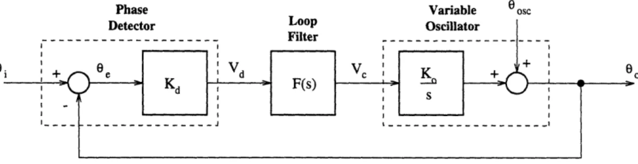
Detector Loop Variable
Filter Oscillator
0
Figure 3-1: Linear phase-locked loop model
A(0o
Vc
V°
Vc
/J1~~ vco
Figure 3-2: Ideal VCO model and characteristic
3.2 Phase-Locked Loops
A phase-locked loop is a system which aligns the phase of an input waveform to the phase of an internally generated reference waveform. The internal waveform generator is usually implemented as a voltage-controlled oscillator (VCO). To begin with, we will analyze the PLL in it's linear region, when it is frequency-locked to the input waveform.
Most PLLs usually consist of a phase detector (PD), a loop filter, and a VCO. See Figure 3-1 for a block diagram of a PLL. The VCO produces an output frequency which is proportional to the input voltage. Figure 3-2 shows a linear VCO character-istic and a functional model of a VCO. It is useful to define the VCO charactercharacter-istic using a "constant" term w, and a deviation Aw,0. The frequency wc is defined as the
average output frequency when the PLL is in lock, when the input frequency equals the output frequency, or wi = w0. The frequency deviation is
AO = K(VC - Vo)
(3.1)
0oo
Ii
Vd
Gi
0e
Go
Figure 3-3: Ideal phase detector model and characteristic
where K, is the VCO "gain" with units of radians per second per volt, V is the control voltage to the VCO and V,, is the control voltage which maintains the output
Wo.
Since we are interested in the phases and phase differences of various signals within the PLL, the transfer function of the VCO must be defined in terms of phase. Frequency is the derivative of phase, or stated differently, phase is the integral of frequency. Using the notation here
00 = o
AWo
dt (3.2)Any deviation in frequency, which is defined as Awo = wo- wi is integrated over time and scaled by K0. Thus, the output phase of the VCO is
= VcK0 (3.3)
From this equation we see that the VCO inherently adds one pole to the system. The phase detector produces an output voltage Vd proportional to the difference in phase between its inputs. Figure 3-3 shows a linear phase detector characteristic and a functional model of a phase detector. The phase detector output voltage is
Vd = Kd(Oi - 0o) (3.4)
where Kd is the phase detector gain with units of volts per radian and Oi is the phase '?
of the input waveform.
The final block in the PLL is the loop filter. The filter output voltage is
V = F(s)Vd (3.5)
where F(s) typically has a low-pass characteristic. The output of the phase detector is filtered and used to tune the VCO.
A simple example illustrates the operation of the PLL. Assume that the PLL is perfectly locked to the incoming waveform so that w = wi. If the frequency of the input waveform rises slightly, a phase error will begin to build up between the input and VCO waveforms. This phase error produces a voltage which in turn tunes the VCO to a higher frequency, eventually matching the input frequency. Similarly, if there is a phase change on the input waveform, the phase detector produces an error voltage which pushes the VCO waveform in the direction of the phase change, cancelling the phase error.
Continuing with the PLL analysis, we combining Equations 3.3, 3.4 and 3.5 and solve for the closed-loop phase transfer function H(s)
H(s) =
-=K
0KdF(s)
(3.6)
9. s + K0KdF(s)
It is also useful to solve for the closed-loop error transfer function He(s) and the open-loop gain of the PLL, G(s)
H, (s) - (3.7)
G(s) = KdKF(s)(3.8)
All three of these functions are used to study the behavior of the PLL. There are three factors that define the PLL system: the VCO gain, the phase detector gain, and the filter transfer function. The VCO and phase detector gains can only be scaled, so the filter transfer function is used to alter the system behavior, which is analyzed next.
3.3 Loop Filter Selection
The loop filter is a very important piece of the PLL system. The type of filter used in a PLL dictates the overall PLL behavior, and the choice of filter time constants affects the performance.
As previouly stated, the VCO contributes a single pole to the system so that in the simplest PLL implementation in which no filter used, the PLL is a first-order system. The system under this condition can be analyzed using an equivalent filter
transfer function F(s) = 1. Plugging this into Equation 3.6 gives the phase transfer
function for the system
H(s) =
(3.9)
s + KoKd
This shows that effectively there is only one variable that the system designer can specify, K = KKd. In this system the loop gain and bandwidth cannot be inde-pendently specified and thus there is a direct trade-off between specifications such as tracking performance and noise tolerance/rejection. To avoid this large constraint, first-order filters are typically used.
When a first-order loop filter is used, the PLL becomes a second-order system and thus there are two independent variables in the system-the designer can indepen-dently specify the bandwidth and loop gain. It is possible to use a second-order or higher-order loop filters, but this usually is undesired. One reason is that the second-order system is well understood and studied, and thus easier to implement. Also, a second-order system usually has enough flexibility with two parameters to satisfy design specifications. Third-order systems are more complex and can can have more complex stability issues that need to be addressed. A first-order loop filter is the most commonly used PLL filter and will be used in this design.
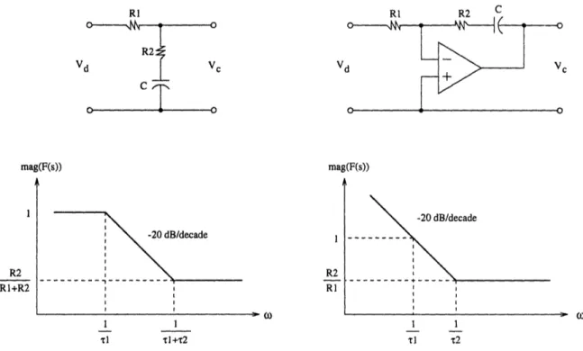
There are two types of second-order filters that can be used, either passive or active, each of which results in a different filter characteristic and PLL performance. Figure 3-4 shows an ideal model for both a passive lag filter and an active Proportional plus Integral (PI) filter, along with their respective transfer functions. The general
RI RI R2 L R2 Vd Vc
(>c
'
-
O
mag(F(s)) mag(F(s)) R2 R1+R2 . -20 dB/decade ~ R1 I R I I I I . 1 1 1 1 Xl l+r2 tl r2Figure 3-4: Passive and active filter models
passive and active filter transfer functions are, respectively
Fp(s) = S r2 + 1 (3.10)
s(ri + r2) + 1
r2+1
F (s) + 1 (3.11) where r1 = R1C and r2 = R2C. There are certain trade-offs between the active and
passive filters. The passive filter is relatively simple to implement, while the active filter has added complexity and must be carefully designed. One advantage of the ideal active filter is that it has infinite DC gain which eliminates the static phase error normally associated with passive filters. The DC gain of the passive filter is unity, or
F(0) = 1. Static phase error is not desirable because it reduces the amount of jitter
that can be tolerated by the PLL while properly re-timing the data.
To analyze static phase error we assume the PLL is in frequency lock with the incoming data stream and that a passive filter with F(0) = 1. In the locked state, the input frequency equals the output frequency, or wi = w. In order to produce this frequency, the VCO must be driven by a certain voltage V,,, which is the control
-20 dB/decade
voltage of the VCO in lock. Since F(O) = 1, this DC control voltage is generated by the phase detector, and assuming an ideal phase detector, this means that there is a static phase error between the VCO and data waveforms. Another source of static phase error is due to the output offset voltage of a non-ideal phase detector. This type of offset voltage is present even if there is no phase error between the VCO and
data waveforms. The static phase error in lock is ,,eo
KdF(O) (3.12)
The static phase error in Equation 3.12 is due to the fixed offset voltage needed to hold the VCO so that wi = w,, which is the locked condition. This design uses an active filter with a very large DC gain-the second term of Equation 3.12 can thus be ignored. We will return to this equation later to make sure that this assumption is valid.
From this point on we assume a first-order active filter, and the active subscript is dropped from the notation. Substituting the active filter transfer function from Equation 3.11 into the phase transfer function Equation 3.6 gives the general second-order PLL phase transfer function
HsKKd
(82+1
H(s)
-
S2 + (KKdTa
(
2) + (KKd)+i)
(3.13)
Using standard servo terminology, the phase transfer function can be written as
2Cw,,s + W2
H (s)
n
- (3.14)s2 + 2w,s + W2 (3.14)
where w, is the natural frequency
=
K
0KX
(3.15)
T 7
mag -40 dB/decade mag K-:ade 1 r2 r2 I- -Ko Kd - Ko Kd x2 T1 1r
Figure 3-5: Second-order PLL open- and closed-loop response
and is the damping ratio of the system
W<: a/~nT~2 ~(3.16)
2
Using the same notation, the closed-loop phase error and open-loop forward gain transfer functions are, respectively
0 e 82
H,(s) = s _ = 2w (3.17)
i s2 2S + w
G
(s)
22(ws +wn (3.18)s2
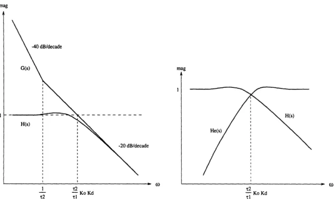
Figure 3-5a compares H(s) and G(s) for a second-order PLL. Figure 3-5b compares
H(s) and He(s) for the same PLL. Notice that as H(s) begins to roll-off at w3dB,
the loop bandwidth, there is a slight peaking in the transfer function. This peaking is a normal phenomenon in second-order systems, and sometimes a bit of peaking is
desired, but in communication systems it can have serious effects and is not tolerated. For example, in long fiber lines that contain hundreds of data regenerators, even
Ii A, \ I I I I I I I I
A1
0
Figure 3-6: Linear phase-locked loop model with VCO phase noise
a small amount of jitter peaking from each regenerator can build up very quickly, eventually resulting in lost data.
3.4 PLL Tracking Performance
The PLL loop bandwidth divides the frequency response up into a high frequency region and low frequency region in which the tracking performance of the PLL must be analyzed. To make the analysis clearer a phase noise source internal to the PLL is included in the linear model. The VCO is a contributor to PLL phase noise as well as other physical noise generators. The resulting phase noise can be lumped together and modeled by VCO noise by adding in o,,, into the system directly after the VCO-see Figure 3-6. The output phase 0, from this model is
2Cws + _ S 2
s2 + 2wns + w2 s2 + 2wns + W2
= H(s) i + H,(s) 0oc (3.19)
Within the loop bandwidth, when s < jW3dB, Equation 3.19 reduces to
82
s = + 2
(3.20)
Equation 3.20 shows that in this region the system tracks changes in i. Also, the VCO phase noise 0,,c below W3dB is attenuated.
Outside of the loop bandwidth, when s > jW3dB, Equation 3.19 reduces to
= S i + o C (3.21)
Equation 3.21 shows that outside the loop bandwidth the system does not track
changes in Gi, and the phase noise from the VCO, 0o,c passes through and appears at
the output.
Referring back to Figure 3-5b, a few things can be summarized. The PLL re-sponse to the input phase Oi determines the jitter transfer and jitter tolerance. These are important specifications in many system designs. To re-time the incoming data properly, the PLL must track slow changes of input phase. This type of phase change may be due to aging, temperature changes, and other wander at the transmitter. Even though the rate of change may be slow, the actual phase changes from these sources may be quite large and span multiple cycles. This is called jitter tolerance because the PLL must track or "tolerate" this jitter without losing lock. This topic will be covered further in later sections. When the rate of phase change is very low the PLL can track these changes perfectly, and H(s) = 1, and thus, the phase error transfer function He(s) is negligible. This also applies to the VCO noise-the PLL can track and eliminate the VCO phase noise below W3dB.
When the rate of phase change from both the input and the VCO approaches and exceeds W3dB, the PLL is not fast enough to track the phase changes. At this point,
H(s) begins to roll-off and the phase error transfer function He(s) approaches
unity-the PLL effectively "ignores" unity-the input phase changes, but as shown previously, unity-the VCO phase noise is seen directly at the output. High-frequency jitter on the input is attenuated (as long as it can be tolerated) which is desirable, but VCO noise may be a problem. If the VCO noise is a problem, steps should be taken to reduce the VCO noise or increase the loop bandwidth. The PLL is usually not required to track changes in the input phase above certain frequencies, and the maximum jitter that
Chapter 4
Phase-Locked Loop Parameter
Calculation
There are two required specifications that constrain the PLL design parameters, jitter tolerance and pattern dependency. We will begin by analyzing the constraints due
to the CCITT pattern dependence test. Next, we will analyze the constraints due to
the SONET jitter tolerance requirements, then combine the constraints. After a brief analysis of jitter transfer, the PLL parameters will be calculated.
4.1 Pattern Dependence Test Constraints
In order to comply with the CCITT STM-N pattern dependence test, the PLL must not lose lock during extended periods of either all O's or all l's bits (See Appendix B, Section B.2). During a "dead" time such as this, unlikely as it may be, there will be no transitions on the serial data line and the phase detector will not be updated-the VCO can drift off frequency, causing a build-up of phase error which may cause the PLL to come unlocked.
It is fairly simple to get an estimate of the maximum phase error due to the required 72-bit long pattern of either all O's or all l's. In the worst case scenario the phase detector is railed at its maximum value during the entire 72-bit period, which corresponds to 28.9 ns. Because the filter transfer function is made up of both integral
and proportional gains, the resulting VCO control voltage has two components, both of which shift the VCO in frequency and thereby cause an accumulation of phase error.
Using the ideal active filter model from Section 3.3, the first contributing source to the filter output voltage is the integral gain of the filter-the filter capacitor integrates the phase error voltage. We define the maximum phase detector offset to be Vdm.z--this is the maximum voltage output from the phase detector when it is railed, which is also Kd for the sample and hold phase detector. The basic capacitor equation is
____p -
I
(4.1)dt C
where I is the current switched through the capacitor, which is
Vdmaz Kd
I =R=R
R1 R11
(4.2)
Integrating both sides of Equation 4.1 and substituting in Equations 4.2 gives
Vcap(t) = R1C (4.3)
The second contributing source to the filter output voltage is the "zero" resistor R2which drops a constant voltage proportional to the input phase error voltage. The
voltage from resistor R2is simply the current I through the resistor or
Ve = VdmaxR2 KdR 2 (4.4) R1 R1
The sum of the capacitor and resistor voltages is applied to the VCO which causes a frequency change, Af. This frequency chage is proportional to the VCO gain K,.
Af(t
=
K.(Vca(t)
(V (t)+Ves)= KKd
(C +R2
(45)
following equation
= 2 A ft) dt (4.6)
Substituting f(t) into this equation and evaluating the integral
AO
= 27r (C +R2) dt = R K 2-C +RT) (4.7)RIdt
R
12C
It is useful to know which PLL parameters influence this phase error. We know from the filter analysis in Section 3.3 that
2 KoKd KoKd (4.8)
W = - (4.8)
71 R1C
R2C = 2 = (4.9)
wn
Plugging these equations into Equation 4.7 gives
A
=
rw.T (nT + 2() (4.10)Given a known maximum allowable Aq, Equation 4.10 becomes
A < rwnT (wT + 2() (4.11)
and we can solve this equation for a solution space. The result gives a curve which defines the allowed values on the (-w plane. Solving Equation 4.11 for wn gives
Wn <
+
T
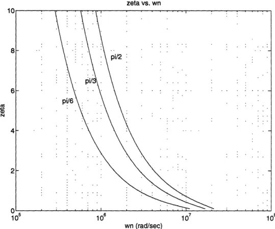
2+ (4.12) Figure 4-1 shows the constant error curves in the -wn plane for phase error limits AO of , , and '. The allowed values for a given phase error limit are below and to the left of the curve. Now we proceed to find the constraints on the PLL parameters due to the jitter tolerance specification.zeta vs. wn
05 lo 10 7 10108
wn (rad/sec)
Figure 4-1: Constant CCITT phase error curves in the (-wn plane
co
4.2 Jitter Tolerance Constraints
As shown in Section 3.4 the jitter tolerance of the system is dependent in part upon the phase error transfer function He(jw). Given a certain level of input jitter at a given modulation frequency Wm, there will be a given amount of phase error on the VCO output. If this phase error is large enough the data will be mis-timed or the PLL might lose lock. The SONET standards specify a minimum jitter tolerance mask-a
minimum amount of jitter that must be tolerated at the input of the PLL without
losing data.
To analyze the constraints on the PLL parameters due to the jitter tolerance spec, we first calculate the magnitude of the phase error transfer function. Plugging s = jwm into Equation 3.17 gives
2 -w
He(Wm)
=
-
+
2wjw +
w
(4.13)
The magnitude of He (jwm) is 2 He(jWm) = )2 + (2 ) (4.14) The phase error qie is simply the magnitude of the phase error transfer function multiplied by the input jitter Omqbe = jHe(jwm) Om =n (4.15)
2 w2 )2 + (2CWnum)2
The SONET jitter tolerance spec is a jitter vs. frequency graph as shown in Figure B-2. In order to construct a solution space and extract a -w, curve similar to the one derived in Section 4.1, Equation 4.15 is evaluated over the SONET spec curve using a math analysis package. The SONET spec is entered into two vectors, a frequency vector w, containing all of the test points, and a phase vector 8, which corresponds to the input jitter at these test points. The function created in the math analysis package has three arguements, , w,, and the phase error limit. When
zeta vs. wn
as
N
105 1o 107
wn (rad/sec)
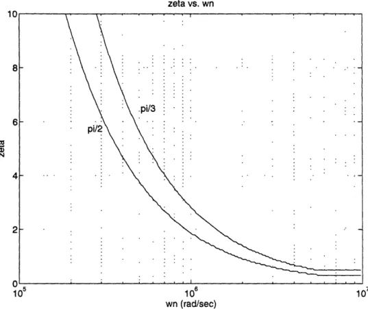
Figure 4-2: Constant SONET phase error curves in the -wn plane
the function is called it simply calculates the phase error vs. frequency curve in response to the SONET spec input jitter at the specified ((,w) point, and checks if the phase error exceeds the phase error limit at any point. If the phase error does not exceed limit, then that (,wn) point is included in the solution space. The entire (-w,
plane can be scanned with this function to construct the solution space, and constant maximum phase error curves can be extracted from this space.
Figure 4-2 shows the and constant phase error curves resulting from the SONET jitter tolerance analysis. The allowed values of ( and w, are above the curve in this graph. The minimum possible value of phase error is 3. This is the high-frequency SONET jitter tolerance level, and corresponds to nearly the same curve as the one given by in Figure 4-2.
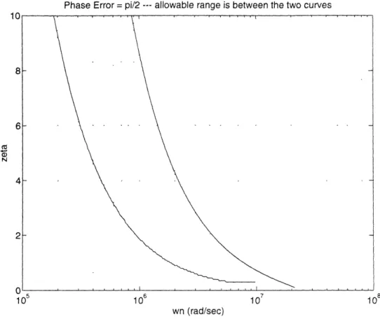
Phase Error = pi/2 --- allowable range is between the two curves
1a
N
103 10° 10' 10
wn (rad/sec)
Figure 4-3: Allowed parameter range to guarantee a phase error of less than '
4.3 Phase-Locked Loop Parameter Curves
The curves from Figure 4-1 and Figure 4-2 are combined and the overall allowed values of ( and w, are between the two curves. Figure 4-3 shows the allowed values of ( and w, for a maximum phase error of 2. The allowed values are between the curves.
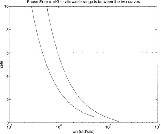
Similarly, Figure 4-4 shows the allowed values of ( and w, for a maximum phase error of . There is no advantage in choosing a point much higher than the 3' 3 SONET curve because it does not decrease the phase error after that point. For this reason we take the SONET curve at the minimum phase error to be the constraint curve. The (C,wn) point selected should be slightly above the SONET curve to ensure a bit of error margin. With this analysis we have essentially found a solution curve, which results in an infinite number of possible (¢,wn) points. In order to further constrain the choices we now consider the SONET jitter transfer specification.
1
a)
N
Phase Error = pi/3 --- allowable range is between the two curves
wn (rad/sec)
Figure 4-4: Allowed parameter range to guarantee a phase error of less than 3 )8
4.4 Jitter Transfer Constraints
The jitter transfer specification is not a requirement for this project because of the
application, but it is useful to further constrain the PLL parameter selection and
increase the performance of the system. The SONET standards call for a jitter transfer function that has a maximum peak of 0.1 dB and a maximum -3 dB point of 2 MHz. Given the jitter peak specification, we can solve for a minimum (.
The jitter transfer characteristic is simply the magnitude of the jitter transfer function, H(jw) 2Cwjw + w
H(jw)
=_o
2+ 2(
njw
+ wc
(4.16)
(2¢w,,)2 (.24 IH(jw)I = (2_co2) 2 + (n)2 (4.17) (W2 - w2)2+ (2Cww) 2To find the peak magnitude we take the derivative of IH(jw) I and set it to zero. Since squaring is a monotonic function, we can simplify the math by taking the derivative of IH(jw)l2 and set it to zero, which will give the same result.
d 2 -4wcco(2(2w 4 - W4o + w2W)
-I
H(jw)lI = (4 2w 2n ± 2. ±+n)-0
(4.18)dw (4W2WC 2 + 4 - 22 + o4)2
The value of w that solves this is the frequency of the peak, w,
cp = 2 N- I (4.19)
where
a= 1
+
8
2
(4.20)
Substituting this result back into Equation 4.17 gives us the magnitude of the peak
Solving this for zeta gives
=
(M
)Mp-/ V a-1
(4.22)
This shows that the magnitude of the phase transfer function peaking is a direct function of (. Using the SONET spec of Mp = 0.1 dB gives = 4.32, but given a 20% margin for error = 5.18 is chosen. Using the curves calculated in Section 4.3, a ( of 5.18 gives a minimum w, of about 6.2 x 10⁵ rad/sec or 95 kHz. Again allowing about 20% margin for error w, = 7.5 x 10⁵ rad/sec or 120 kHz is chosen.
Now we can solve for the 3 dB point of the magnitude of the phase transfer function
IH(jw)i = 2)2 + (2( )2 (4.23)
(W - w2)2 + (2Cwnw)2 =
2
and now solving this for w gives the 3 dB point in terms of wnW3dB = n /l + 2 + 2 +
4
2+
44 (4.24)Substituting wJ = 7.5 x 10⁵ rad/sec gives a loop bandwidth W3dB = 7.8 x 10⁶ rad/sec or 1.2 MHz. From this analysis we can see that the PLL can meet the SONET jitter transfer specification even though the intended application of this system does not require this specification.
Chapter 5
Clock Recovery and Data
Re-timing Circuit Design
The clock recovery subcircuit is the heart of the receiver project. Without it, the correct phase and frequency clock cannot be extracted and the serial data cannot be recovered. The design of this block is very sensitive, and if it is not designed properly, the resulting bit error rate will be too large for practical use.
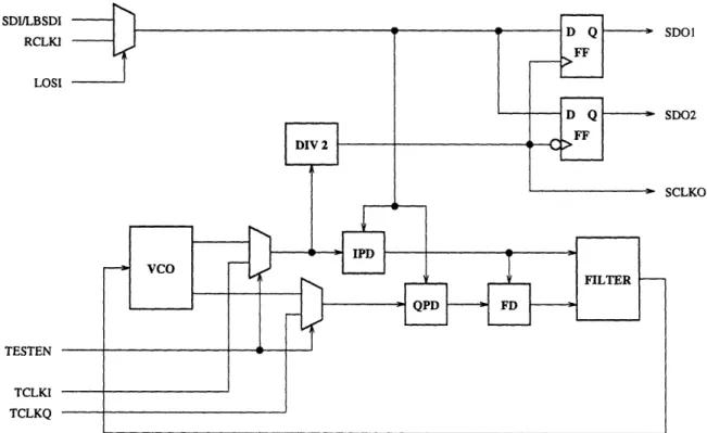
A block-level diagram of the clock recovery and data retiming system is shown in Figure 5-1. The inputs to this system consist of the high-speed serial data (either SDI or LBSDI), a low-speed reference clock (RCLKI), the Test Enable line (TESTEN) and the corresponding Test Clock In-phase and Quadrature lines (TCLKI and TCLKI), and a Loss-Of-Signal Indicator (LOSI) line. During normal operating conditions LOSI will be low and the PLL will lock to the high-speed data input, but when the LOSI line is asserted, the PLL switches over and locks onto the reference clock input to provide a stable clock output.
The high-speed PLL locks onto the 2.48832 Gb/s NRZ data, which can be thought of as a 1.24416 Ghz pseudo-sinusoid. The extracted clock signal is a phase-locked 2.48832 Ghz clock which is divided down to 1.24416 Ghz because the downstream circuitry (frame detect, demux, etc) uses both edges of the clock, instead of just a rising edge. To re-time the data, two flip-flops which operate on opposite clock edges are clocked from the VCOI signal divided down by 2.
SDI/LBSDI RCLK LOSI TESTEN TCLKI TCLKQ SDO1 SD02 SCLKO
Figure 5-1: Block Diagram of the clock recovery and data retiming system
5.1 Phase and Frequency Detection
The FPLL uses an interesting phase and frequency detection scheme, derived from an article by Ansgar Pottbacker, et al[5]. Pottbicker states the benefits of using this scheme-it uses a relatively simple and low-speed phase and frequency detection system, no pre-processing of the NRZ data stream is needed, and a half-bit delay generator is not needed. See Figure 5-2 for a simplified diagram of the Pottbicker
FPLL.
The phase-frequency detector requires a VCO that produces in-phase and quadra-ture outputs. In Pottbicker's paper, the two phase detectors (IPD and QPD) are essentially digital samplers which sample on both edges of the input clock. Instead of using the VCO waveform to sample the data stream, like typical digital phase detectors, the serial input data is used as a clock input to the phase detectors which sample the VCO waveforms-one phase detector samples the in-phase VCO wave-form (VCOI) and the other phase detector samples the quadrature VCO wavewave-form (VCOQ). First we assume that the VCO is not frequency-locked to the data.
Fig-Figure 5-2: Block Diagram of the FPLL Q1 lQ2 Q3 Rising 1 0 Falling 1 0 Rising -1 -1 Falling -1 1
Table 5.1: Frequency detector state table
ure 5-3(a) shows a timing diagram for the phase detectors when the VCO frequency
fvo, is higher than the bit rate fb, and Figure 5-3(b) when the VCO frequency is lower
than the bit rate. In the un-locked condition, the sampled Q1 and Q2 waveforms are the beat notes between the VCO and data frequency, and the Q1 and Q2 signals will always be in a quadrature relationship with one another--one signal will lag the other by 90 degrees-but which signal lags and leads depends on the sign of the frequency difference between the data and the VCO. Figure 5-3(a) shows that when f,,, > fb,
Q1 leads Q2 by 90 degrees, and in Figure 5-3(b) when f,,o < fb, Q2 leads Q1 by 90 degrees. The frequency detector (FD) processes these quadrature beat notes, and depending on their quadrature relationship, the DC average of the Q3 output is the sign of the frequency difference. Table 5.1 shows the state table for the frequency detector which results in the proper beat note processing. The Q3 signal, after pass-ing through the loop filter, drives the VCO towards lock. Notice that the FD output only changes state on a transition of Q1, either rising or falling, and that the FD has a ternary output, either 1, 0, or -1. Referring back to Figure 5-3, the FD output
acp
DATA Qll VCOQ VcOQ r\ i I A L 1 LX Al 1 DATA I r r \ - t Q3 \/
~^~
X ....
... 'i"
...
.~
-VCO ,i , , ;- ,t Q1 I. f I F Q2 __ Q3 I i/\ ,Figure 5-3: Timing diagram of the FPLL out of frequency lock
t
DATA VCOI VCOQ = A. _, I = A. t DATA I I . ! I .... I I' l l l I l I I , I l l ~ ~~~ ~ ~~~ ~ ~~~ ~ ~~~ ~ ~~~ ~ ~~~ ~ ~~ ~ ~~ ~ ~~~~~~~~~~~~~~~~~~~~~~~~~~~~~~~~~~~~~~~~~~~~~~~~~~~~~~~~~~~~~~~~~~~~~~~~~~~~~~~~~~~~~~~~~~~~~~~~~~~~~~~~~~~~~~~~~~~~~~~~~~~~~~~~~~~~~~~~~~~~~~~~~~~~~~~~~~~wt VCO1 a - W h a t ,
~ ~ ~ ~ ~ ~
~
l\ . , IFigure 5-4: Timing diagram of the FPLL in frequency lock when the phase error is zero (a) and slightly off phase (b)
with these properties can be thought of as cancelling a half-cycle of the Q1 waveform when Q1 and Q3 are summed together, resulting in a DC component which drives the VCO towards lock. Figure 5-3 also shows that the proper waveform processing still occurs even if there are missing transitions in the data waveform.
Now we will look at the case when the FPLL is in both frequency and phase lock, or fco = fb and the phase error is exactly zero. See Figure 5-4(a). In this ideal case,
the falling edge of the VCOI waveform is aligned exactly with each transition in the data stream-the in-phase PD (IPD) clocks in Q1 = 0 (or "metastable" state) and the quadrature PD (QPD) clocks in Q2 = 1. Again referring back to Table 5.1, this is the state in which the FD is not active (Q3 = 0) and contributes nothing to the phase error signal. This results in a stable operating point and a perfect lock when Q1 = 0 and Q3 = 0. In reality, jitter on both the data and VCO waveforms shifts the data and VCO edges slightly which toggles Q1 between -1 and 1 randomly. This is also a stable operating point because the DC average of Q1 is zero.
Now we will assume that the FPLL is in frequency lock but not in phase lock. This will be the case if the VCO begins to slide off-phase as shown in Figure 5-4(b). In this case the IPD responds as a phase detector whose output voltage corresponds to the sign of the phase difference. This type of phase detector is known as a "bang-bang" phase detector because of it's digital behavior. There are certain advantages and disadvantages of using a bang-bang type phase detector which will be discussed later. Notice that as long as the phase difference (or jitter) is less than 90 degrees of the VCO waveform, Q2 remains in state 1 and the FD does not become active. Referring to Table 5.1, the frequency detector remains inactive until the VCO drifts
I
I I I I
-WAVEFORM IN CLK ANALOG MUX OUT
Figure 5-5: Sample and hold phase detector
180 degrees off phase which corresponds to a transition of Q1 when Q2 = 0.
Under normal frequency-locked operation, the transitions of the data waveform will be jittering around the VCOI falling edge slightly. This causes the appropriate phase error signal to be generated, but again, as long as the phase jitter is kept within a ±7r range no frequency error signal is generated.
5.2 Phase and Frequency Detector Design
A high-performance analog sample-and-hold circuit is used as the phase detector. The sample-and-hold phase detector design is based on the same concept as the flip-latch. The circuit contains two track-and-hold analog "latches" and a 2:1 multiplexer, as shown in Figure 5-5. Appendix D covers the basic operation of this type of sample-and-hold phase detector. Each track-sample-and-hold block is based on the diode bridge topology. Because the diode bridge is a single-ended topology, each of the track-and-hold blocks consist of two separate diode bridge circuits, one for each of the differential lines. Because of this symmetry, only one of the two diode bridge circuits from each track-and-hold is analyzed.
Figure 5-6 shows the basic diode bridge topology. The main sampling diode bridge consists of diodes D1 through D4. Transistors Q1 and Q2 form a current switch which switches the diode bridge from hold mode to track mode and vice versa, and diodes D5 and D6 are clamping diodes for operation in the hold mode. Inputs trackh and trackl
VCC
VINL VOUTL
VEE
Figure 5-6: One half of a differential track and hold circuit
are the high and low sides of the digital differential track signal, respectively. First, lets analyze the circuit in track mode, when (trackh - trackl) > 0, so that current switch transistor Q2 is cut-off and Q1 conducts a current of 2I. When the input is at
about the same voltage as the output, the current is split equally between the right
and left hand sides of the diode bridge, as shown in the simplified Figure 5-7(a). In this state all of the diodes are conducting and have equal voltage drop, resulting in zero offset from input to output. Also, in this state the input supplies zero current. Because the input and output signals are one half of a differential signal, input to output offset is not a problem within certain limits.
The analysis of the diode bridge dynamics in track mode must be broken into two parts, the first when the input is approximately equal to the output, and second when there is a large difference between the input and output (when the circuit switches from hold to track mode for instance). When the input within a few kT q of the output,
the diodes can be modeled simply as resistors of value rd = D. In this case the time constant associated with the holding capacitor C1 is due to the resistance of the
VCC
VCC
I
2 2
VINL VOUTL VINL
VEE VEE
Figure 5-7: Simplified diode bridge in track mode
"resistor network" seen by C1.
2kTC1
r
=
rdC1
=
kTC
(5.1)
qI
When the input is greater than (or less than) a few kT q from the output, the limiting factor in charging time is the slew rate due to the maximum current I available at the output. Figure 5-7(b) shows the diode bridge when the input is at a much higher voltage than the output. In this case diodes D2 and D3 carry nearly all the current and the capacitor is charged with a constant current I, resulting in a slew rate of
I/C. One disadvantage of this is that the input must also provide a current of I,
therefore a unity-gain buffer with a high current drive capability is needed to drive the track-and-hold circuits.
Referring back to Figure 5-6, when the circuit is in the hold mode, or when
(trackh - trackl) < 0, transistor Q1 is cut-off and Q2 conducts a current of 2I. In
this mode, current I flows through diodes D5 and D6 which reverse biases diodes D1 through D4 by -VBE. The back-to-back reversed biased diodes D1-D2 and D3-D4 effectively disconnects the input and output. Leakage currents from the diodes will tend to charge or discharge C1 and cause errors. Similarly, any input current
needed for the output buffer which follows the track-and-hold will tend to charge or discharge the capacitor. If a standard emitter follower is used, current will be drawn
VOUTL VCC I I I I I
VlP
VOUTL
(P+1) P
VEE VEE VEE
Figure 5-8: Modified track and hold circuit
out of the capacitor, causing the output voltage to decrease linearly with time. As long as matching between devices is good the resulting errors will be seen only as a common-mode error which will be rejected by the following stages.
In order to improve the tracking capability, it is desirable to use a small charging capacitor along with high bias current. When a small capacitor is used however, the capacitor will discharge faster in the hold mode due to the input current required for the following buffer stage. As previously stated, this results in a common-mode offset, which is not a problem, but the capacitor voltage should not drift significantly over a length of time when there are no data transitions. For example, with random data input into the phase detector there is no guarantee that the next data edge will occur within a bit period or two, and thus the hold mode could last for many bit periods before switching back into track mode.
A few modifications to the track and hold circuit are shown in Figure 5-8. In this diagram the output buffer is included, and the bias currents are shown. With the current cancelling circuitry, the input current to the buffer is reduced by about a