HAL Id: hal-02976031
https://hal.archives-ouvertes.fr/hal-02976031
Submitted on 23 Oct 2020
HAL is a multi-disciplinary open access
archive for the deposit and dissemination of
sci-entific research documents, whether they are
pub-lished or not. The documents may come from
teaching and research institutions in France or
abroad, or from public or private research centers.
L’archive ouverte pluridisciplinaire HAL, est
destinée au dépôt et à la diffusion de documents
scientifiques de niveau recherche, publiés ou non,
émanant des établissements d’enseignement et de
recherche français ou étrangers, des laboratoires
publics ou privés.
Preparation and study of CuBi2O4 thin films by RF
magnetron sputtering
Benjamin Duployer, Christophe Tenailleau, Yohann Thimont, Pascal
Lenormand, Antoine Barnabé, Lionel Presmanes
To cite this version:
Benjamin Duployer, Christophe Tenailleau, Yohann Thimont, Pascal Lenormand, Antoine Barnabé,
et al.. Preparation and study of CuBi2O4 thin films by RF magnetron sputtering. Materials Research
Bulletin, Elsevier, 2020, 130, pp.0. �10.1016/j.materresbull.2020.110940�. �hal-02976031�
OATAO is an open access repository that collects the work of Toulouse
researchers and makes it freely available over the web where possible
Any correspondence concerning this service should be sent
to the repository administrator:
[email protected]
This is an author’s version published in:
https://oatao.univ-toulouse.fr/26834
To cite this version:
Duployer, Benjamin and Tenailleau, Christophe and Thimont,
Yohann and Lenormand, Pascal and Barnabé, Antoine and
Presmanes, Lionel Preparation and study of CuBi2O4 thin films by
RF magnetron sputtering. (2020) Materials Research Bulletin, 130.
ISSN 0025-5408
Open Archive Toulouse Archive Ouverte
Official URL :
Preparation and study of CuBi
2
O
4
thin
films by RF magnetron sputtering
Benjamin Duployer, Christophe Tenailleau
*
, Yohann Thimont, Pascal Lenormand,
Antoine Barnabé, Lionel Presmanes
CIRIMAT, Université de Toulouse, CNRS, Université Toulouse 3 - Paul Sabatier, 118 Route de Narbonne, 31062 Toulouse Cedex 9, France
A R T I C L E I N F O Keywords: Thinfilm CuBi2O4 Bi2CuO4 Sputtering Band gap Raman spectroscopy Optical constants n and k
A B S T R A C T
Copper bismuth oxide (CuBi2O4or Bi2CuO4) thinfilms have been elaborated for the first time by radio-frequency magnetron sputtering using a homemade CuBi2O4ceramic target. X-ray diffraction characterizations revealed an amourphous phase for as-depositedfilms. After air annealing at 450 °C for 12 h, a pure polycristalline CuBi2O4 phase can been obtained. Raman spectroscopy confirmed the film phase purity. The influence of the thickness on the structural properties of thefilms has been studied and we observed that all films treated above 450 °C are crystallized. The thinnerfilms show preferred orientation while there are less crystal defects for the thickest films (∼700 nm). Atomic force microscopy shows a homogeneous polycristalline microstructure at the surface of the film. Optical measurements performed by UV–vis-IR spectrophotometry indicate that these films have one of their optical band gaps in the visible region (Eg∼1.5 eV) which makes them suitable as thin films solar ab-sorption materials.
1. Introduction
The ternary compound CuBi2O4possesses an unusual crystal
struc-ture with stacks of square planar CuO4groups linked to distorted
tri-gonal BiO6polyhedra, associated with very interesting electrical and
antiferromagnetic properties [1,2]. In recent years, this p-type semi-conductor has been identified as a promising material for its use in photocatalystis, photoelectrochemistry and the generation of hydrogen from water [3–5]. Indeed, it was reported that CuBi2O4has an optical
absorption onset of 1.4–1.8 eV although it is not yet clear whether the band gap is direct or indirect [6]. Moreover, its conduction band minimum is located on a more negative position than the water re-duction potential, enabling solar H2production [7–9].
Up to now, all CuBi2O4thin films reported were synthesized by
electrodeposition [10,11], hydrothermal synthesis [8], sol gel method [12], or spray pyrolysis [13], essentially. Among all deposition methods, sputtering deposition (Physical Vapor Deposition or PVD) is a simple, industrial and environmentally friendly technique that can provide dense and homogenous oxide thinfilms with a good control of their thicknesses and excellent adhesion. A post-thermal annealing has often to be carried out in order to get a fully crystalline material. In the case of stable oxides, this thermal annealing can be a simple and con-ventional annealing treatment performed in air, which is less expensive than thermal annealing under vacuum, neutral gas, or complex atmo-sphere. By easily controlling the sputtering parameters, playing on the
pressure to vary the porosity for example [14], the properties of the films can be optimized for various applications.
However, to the best of our knowledge there is no publication yet about the use of the radio-frequency (RF) sputtering technique for its deposition.
In this work, we thus report for thefirst time the preparation of CuBi2O4thinfilms by the PVD technique and their structural,
micro-structural and optical characterizations. 2. Experimental
2.1. Film preparation
Thin films were deposited by RF magnetron sputtering using a homemade CuBi2O4ceramic target. Indeed, a stoichiometric mixture of
CuO and Bi2O3commercial powders wasfirst heated at 770 °C (below
the eutectic point) for 48 h in air to get a pure CuBi2O4phase (checked
by X-ray diffraction). The polycrystalline CuBi2O4powder (150 g) was
then pressed in a die of 10 cm in diameter and sintered at 770 °C for 12 h under air atmosphere. The relative density of the target was about 75 %. X-Ray Diffraction (XRD) measurements carried out on a small re-presentative pellet showed no impurity phase.
The sputtering apparatus is an ALCATEL A450 with a radio-fre-quency generator (13.56 MHz) and a pumping system (limit pressure P = 5.10−5Pa inside the deposition chamber before deposition). The RF
⁎Corresponding author.
E-mail address: [email protected](C. Tenailleau).
power was fixed at 20 W. Pre-sputtering by argon plasma was per-formed during 15 min to clean the target surface of any impurity prior to the film deposition. Pre-cleaned 1 mm thick microscopy slides, convenient due to their high transparency, intermediate thermal dila-tation coefficient and low cost, were used as substrates.
The deposition parameters are summarized inTable 1. The analysis of the chemical composition of thefilms made by electron probe micro-analysis (using a Cameca SX 50 apparatus) confirmed the conservation of the target composition into thefilm. The sample showed a Cu/Bi ratio close to 0.5 and a general formula of Cu1.02(4)Bi1.9(2)O4.10(4) was determined for all samples analyzed.
Thickness measurements were performed by surface profilometry, using a DEKTAK 3030ST mechanical profilometer, and by X-Ray Reflectivity (XRR), using a Bruker D8 Advance diffractometer equipped with a Göbel mirror. The experimental XRR data were fitted using a modified Fresnel recursive formula, generally referred as the Parratt formalism [15]. All measurements we made on as-deposited samples. 2.2. Characterizations
Structural characterizations offilms were performed using a Bruker D8 diffractometer in the Bragg-Brentano configuration. Data were re-corded using a CuKαwavelength radiation (40 kV, 40 mA) and
col-lected over the 10° < 2Θ < 100° range at room temperature with a 0.02 step scan and 20 s/step. Nickelfilter was used to eliminate the Kβ-ray
and reducefluorescence.
Raman spectra were collected under ambient conditions using a LabRAM HR 800 Jobin Yvon spectrometer with a laser excitation wa-velength of 532 nm. Spectra acquisitions were carried out for 300 s using x100 objective lens and 600 g/mm grating. Examination of multiple spots showed that the deposited sample were homogeneous.
To study the microstructure of thefilms, Atomic Force Microscopy (AFM) Veeco Dimension 3000 equipped with a super sharp TESP-SS Nanoworld tip was used. AFM surface images were analysed using the Gwyddion Software.
The electrical measurements were made with a QuadPro four-point probe device from Signatone equipped with a Keithley SMU 237. This type of system can measure a maximum resistance of 1010Ω.
The optical characteristics of thin films were investigated in the 300–1100 nm wavelength range using a Bentham PVE300 integrated spectrophotometer. The optical transmittance of the glass substrate was systematically subtracted from thefinal data before calculation. Spectra were then modeled using the SCOUT software [16].
3. Results and discussion 3.1. Thickness determination
To calibrate the thicknesses of the layers, we used two different techniques. First, an uniform deposition rate equal to 6.25 nm.min−1in the 25–700 nm range has been determined by measuring walking
heights with a mechanical profilometer. We then proceeded to XRR measurements for showing that our deposition technique can be used for the preparation of a dense, controlled in thickness and homogenous thin layer of CuBi2O4.
From the Parratt’s formalism and in the case of one simple layer, the specular reflection coefficient R is expressed as:
= + + − − R r r e r r e 1 ik d ik d 1 2 2 1 2 2 2 2 2
Where r1an r2are the Fresnel reflection coefficient for respectively the
air/layer (r1) and the layer/substrate (r2) interfaces, k2the wave
vec-tor’s normal component of the electromagnetic wave propagating in the layer and d the thickness.
The Fresnel reflection coefficient depends upon the incident angle in between the beam and the sample surface as well as the refractive index of the considered material. When the chemical composition is well-known, the refractive index is expressed depending on the density. So thefit of the experimental data has been done by considering both thickness and density as adjustable parameters.
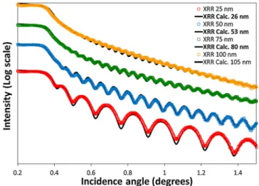
Fig. 1shows the X-Ray Reflectivity curves for samples with theo-retical thicknesses of 25 nm, 50 nm, 75 nm and 100 nm. These curves exhibit well marked oscillations, known as Kiessig fringes [17], which are characteristics of continuous, homogenous and uniform layers with low surface and interface roughness. Full lines correspond to the best fitting curves from which the thickness and the density are deduced. The values obtained (26 nm, 53 nm, 80 nm and 105 nm for thicknesses; 8.4 g.cm−3for density) are very close to the theoretical ones. This confirms that it is possible to produce thin films with a precise and homogeneous thickness and a high density using the sputtering tech-nique, which is an important advantage over other deposition techni-ques.
3.2. Structural and microstructural characterizations
Thicker samples have been studied in order to have a better dif-fraction signal and to better characterize the purity of the thinfilm.
The substrates used in this work were microscopy slices, made out of 1 mm thick soda-lime glass (∼ 5 cm2square substrates). Although
the softness temperature is usually around 750 °C, according to some supplier references, it can be around 550 °C, close to the treatment temperature chosen in this paper. In addition, this choice was also justified by the fact that most of the n-type TCOs on which our material could be superimposed for future electronic and energy applications are stable in this temperature range.
Afirst sample of 700 nm has been first deposited and studied.Fig. 2
Deposition parameters Target Diameter (cm) 10 Target-to-substrate distance (cm) 5 RF power (W) 20 Magnetron yes Sputtering gas Ar
Background pressure (Pa) 5.10−5 Working pressure (Pa) 0.5 Argonflow rate (sccm) 11 Deposition rate (nm. min−1) 6.25 Film thickness (nm) 100−300-700 Substrate holder water cooled
Fig. 1. X-Ray reflectivity curves for a CuBi2O4thinfilm. Full line is the best fit calculated from the recursive Parratt formalism.
Table 1
shows the XRD patterns of CuBi2O4thinfilms studied (as-deposited and
annealed under air at 400 °C and 450 °C for 12 h). The as-deposited sample shows no diffraction peak which indicates an amorphous or nanocrystallized sample.
From 400 °C, thefilm begins to crystallize. Peaks of low intensity correspond to the crystalline structure of CuBi2O4, whereas the broad
hump in the background shows that there is still some amorphous phase that remains, thus evidencing that this temperature is not sufficient to have a good crystallization for this lap of time.
It is from twelve hours of annealing at 450 °C in air (suitable tem-perature for a glass substrate) that the sample has the best crystallized state and the XRD diffraction pattern corresponds to the reference pattern # 00-042-0334 of the ICDD Powder Diffraction File (PDF®)da-tabase. This result shows that thefilm consists of a pure polycrystalline CuBi2O4with a tetragonal crystal structure (P4/nnc space group). Our
cell parameters determined at room temperature by profile matching using the Fullprof Sofware are a = 8.4945(7) Å and c = 5.8199(5) Å [18]. An apparent crystallite size of 70 nm has been estimated from the total Full Width at Half Maximum (FWHM) considering only the main (211) Bragg peak corrected from the instrumental contribution (i.e. assuming that the microstrain are negligible), applying a pseudo-dis-tribution for the peak broadening, and using Scherrer’s formula:
= D λ FWHM θ 0.9 cos sample
whereD is the crystallite size, FWHMsample is the full width at
half-maximum corrected from experimental broadening,λis the X-ray wa-velength (1.54056 Å) and θ is the Bragg angle.
This 700 nm thinfilm annealed at 450 °C has been also investigated by Raman spectroscopy. A comparison with our reference powder used for the target was made and the spectra are depicted in Fig. 3. The sputter-deposited film shows exactly the same spectrum than the CuBi2O4target. This demonstrates that the sputtering technique did not
modify the stoichiometry of the compound. These results are also in agreement with the literature. Indeed our samples show the same fea-tures than for a bulk sample of CuBi2O4synthesized by the traditional
solid-state reaction method in air and reported by Popovic et al. [19]. Eight Raman bands are observed and centered at 80, 130, 189, 263, 283, 406, 466 and 589 cm−1. The band at 80 cm−1corresponds to the B2gmode and is attribued to in-plane bond bending vibration of the
rhombohedra. The strong peak at 130 cm−1represents the A1gmode
which originates from translational vibrations of the CuO4planes along
the z axis. The small peak at 189 cm−1is the Egmode and indicates the
vibration of Cu-Cu links. The A1gmode at 263 cm−1corresponds to the
rotation of two staked CuO4squares in opposite directions. The peaks at
280 cm−1and 466 cm−1, corresponding to B2gmodes, are assigned
mainly from the oxygen motion. The band observed at 406 cm−1is the
A1gmode of the Bi-O stretching vibration while the peak at 589 cm−1is
an in-plane breathing of CuO4squares.
These two complementary structural characterization techniques (XRD and Raman) show that it is possible to produce 700 nmfilms of CuBi2O4using the sputtering technique. With a simple annealing stage
at 450 °C in air, we can obtain well crystallizedfilms with very high purity.
After optimization of the crystallization temperature, the influence of the thickness on the structural properties of thefilms was studied. XRD patterns of the CuBi2O4films with 3 different film thicknesses are
shown inFig. 4.
Allfilms are polycrystalline, and the major peaks corresponding to the tetragonal CuBi2O4(PDF®. # 00-042-0334) are observed. The cell
parameters a and c, determined at room temperature by profile matching, are reported inTable 2. The values are in good agreement with the reference PDF® pattern and no signifiant effect of the thickness on the cell parameters is observed.
In order to have information about the level of crystallinity in these films, one can look at the evolution of the crystallite size (D) and the dislocation density (δ) according to the thickness.
The dislocation density, defined as the length of dislocation lines per unit volume of the crystal, was evaluated from the formula [20] :
=
δ D
1 2
All of these values, calculated for the most intense (211) diffraction peak, are given inTable 2.
Fig. 2. X-Ray diffraction patterns of thin films as deposited and annealed at
different temperatures. Fig. 3. Raman spectra of CuBi2O4powder and thinfilm (700 nm after annealing
at 450 °C).
Fig. 4. X-Ray diffraction patterns of CuBi2O4thinfilms for various thicknesses. Insert shows the variation of the texture coefficient for different (hkl) planes.
The crystallite size of thefilms increased from 35 to 70 nm with increasing thickness. The low dislocation density value for a thickness of 700 nm confirms the good level of crystallization, with less crystal defects in eachfilm.
Fig. 4also shows a significant effect of the film thickness on the diffraction peak intensity ratios. Indeed, all the peak intensities increase proportionally with the thickness except for the (211) and (422) or-ientations. Harris’ relation can be used to understand the quantitative relation between the peak intensity and orientation [21]:
= ∑ − TC(hkl) N I(hkl) I (hkl) 1 I(hkl) I (hkl) 0 0
where TC(hkl), known as the texture coefficient, qualitatively defines the preferential orientation of the thinfilm. I(hkl) is the intensity of a particular plane from the recorded XRD pattern and I0(hkl) is the
in-tensity of the corresponding plane from a standard ICDD pattern. N is the number of diffraction peaks used in the calculation.
Insert inFig. 4 shows the variation of the texture coefficient for different (hkl) planes. We can observe a strong preferred orientation for the (211) plane that decreases when the thickness increases from 100 nm to 700 nm. In other words, if thefilm grains are preferentially or-iented, an anisotropy of the material properties could then be observed. AFM images of CuBi2O4 thin films have been taken in order to
complete the microstructural information and confirm these results (Fig. 5). A 700 nm as-deposited sample and three others of 100 nm, 300 nm and 700 nm annealed at 450 °C are here compared.
From these images, we canfirst see the significant effect of an-nealing on the microstructure of the samples. Indeed, for the 700 nm sample, the surface grain diameter increased after annealing at 450 °C, in comparaison to the as-deposited sample. The in-plane average grain size was estimed by an immersion threshold method thanks to the Gwyddion software [22]. The mean diameter increased from 20 nm for the as-deposited sample to 60 nm for the annealed sample. This grain size is close to the value of the crystallite size determined by XRD.
It is also noted that the thickness influences the homogeneity and the density of thefilm. In fact, the thinnest films seem to be composed of aggregates with a fairly large dispersion. The roughness decreases with thickness. With a Ravalue of 9 nm for the 100 nmfilm to 5 nm for
the thickestfilm (700 nm). The images also seem to show much more grain boundaries and pinholes for the 100 nm and 300 nm samples than for the 700 nm film. These observations are in agreement with the values of dislocation density calculated previously.
3.3. Electrical and optical properties measurements 3.3.1. Electrical resistivity
The plots of the I–V characteristics are shown inFig. 6. Measure-ments have been made at room temperature, 100 °C and 150 °C for films of different thicknesses. However, it can be noted that for the 100 nmfilm the measurements are only possible from 150 °C and for that of 300 nm from 100 °C. The resistance values are otherwise too high for the system. The linear nature of the I–V charateristics confirms an
Thickness (nm) FWHM (degrees) Crystallite size D (nm)
Dislocation densityδ (nm−2) Cell parameters a (Å) c (Å)
100 0.278 35 8 × 10⁻⁴ 8.5129(5) 5.8155(8)
300 0.177 60 3 × 10⁻⁴ 8.4989(6) 5.8127(6)
700 0.166 70 2 × 10⁻⁴ 8.4945(7) 5.8199(5)
Fig. 5. AFM images of CuBi2O4thinfilms: (a) 700 nm as deposited, (b) 700 nm (c) 100 nm (d) 300 nm after annealing at 450 °C. Table 2
ohmic character of all CuBi2O4films. From these measurements, a
re-sistivity value can be calculated for each thickness and each tempera-ture (given inFig. 6). The observed behavior of the electrical resistivity, with respect to the variation in resistivity, is representive of a con-ventional semiconductor material. Indeed, the resistivity decreases with the increasing temperature. Note that the resistivity is lower for the thickest films, which is probably due to the presence of lower grain boundaries concentration. From this data and for the 700 nmfilm, an activation energy (Ea= 0.24 eV) was obtained, which corresponds to
the separation between the Fermi level and the valence band. 3.3.2. Optical properties
Fig. 7a and b show the integrated Total Transmittance (TT) and Total Reflectance (TR) optical spectra variations of a 700 nm thick film annealed at 450 °C and the corresponding simulated TT and TR spectra. TT and TR spectra werefitted simultaneously thanks to dielectric models, which integrate a Kramer Kronig relationship for interband transition [23] and Kim oscillators [24]. A good match between ex-perimental and simulated TT and TR spectra has been found (standard deviation of 1.6 × 10⁻⁴and 5.8 × 10⁻⁵for TT and TR, respectively)
and the model allowed to obtain a good estimation of thefilm thickness of 685 nm, in agreement with the measurements done by profilometry (690 nm).
The variations of the optical index n and k in the 300−1000 nm range, which have been deduced from this model, are presented in Fig. 7c.The values are similar to those obtained by Manley et al. [25] with a spectroscopy ellipsometer on a single crystal of CuBi2O4.
Using the absorption coefficient deduced from the optical simula-tion, we generated the Tauc plots over the same spectral range (shown in Fig. 8) and determined both direct and indirect bandgap by linear extrapolations to the energy axis.
A direct band gap Egdclose to 3.5 eV can be determined. It would
correspond to the transition between the O2p and Cu3d orbitals.
However, two indirect band gap can also be determined at lower en-ergies with an exponent of 1/2 for the (α.h.ν) vs E by drawing the Tauc plots. The highest band at Egi,1= 2.6 eV would also correspond to a O2p
and Cu3dtransition, while the value of the lowest band energy
transi-tion Egi,2= 1.5 eV would be associated to Bi6sand Cu3dtransitions. The
lowest energy values determined here are in agreement with the p-DOS diagram found in the litterature and calculated by Sharma et al. [8].
This lower bandgap value in the visible range makes those CuBi2O4
thin films deposited by RF sputtering also very interesting for solar energy applications.
4. Conclusion
CuBi2O4 thin films were deposited for the first time by RF
magnetron sputtering and characterized by XRD, Raman, AFM, and UV–vis-IR spectrophotometry measurements. These films, after heat treatment at 450 °C in air, show a pure CuBi2O4 phase with good
cristallinity. The microstructure is homogeneous and dense with a na-nometric grain size. Two indirect optical band gaps were measured at 2.6 and 1.5 eV in accordance with the bulk material. Due to the fact that the post-deposition annealing stage can be carried out at moderate temperature, the RF magnetron sputtering technique can provide an easy access route to cristalline thinfilms of CuBi2O4on glass substrate. Fig. 6. Current–voltage (I–V) curves for CuBi2O4films.
Fig. 7. (a) TT (b) TR optical spectra of 700 nm thinfilms annealed at 450 °C. (c) Optical index n and k plotted as a function of wavelength for the CuBi2O4thin film.
Fig. 8. Plots of (αhν)2and (αhν)1/2as a function of photon energy for the CuBi2O4thinfilms.
Authorship contributions Category 1
Conception and design of study: Christophe Tenailleau, Lionel Presmanes, Benjamin Duployer;
acquisition of data: Benjamin Duployer, Antoine Barnabé, Yohann Thimont, Pascal Lenormand;
analysis and/or interpretation of data: Benjamin Duployer, Antoine Barnabé, Yohann Thimont, Pascal Lenormand, Christophe Tenailleau, Lionel Presmanes;
Category 2
Drafting the manuscript: Benjamin Duployer, Christophe
Tenailleau, Lionel Presmanes;
revising the manuscript critically for important intellectual content: Benjamin Duployer, Antoine Barnabé, Yohann Thimont, Pascal Lenormand, Christophe Tenailleau, Lionel Presmanes;
Category 3
Approval of the version of the manuscript to be published: Benjamin Duployer, Antoine Barnabé, Yohann Thimont, Pascal Lenormand, Christophe Tenailleau, Lionel Presmanes.
Declaration of Competing Interest
The authors declare that they have no known competingfinancial interests or personal relationships that could have appeared to in flu-ence the work reported in this paper.
Acknowledgements
The French FERMAT Federation FR3089 is acknowledged for fi-nancial support to the D8 XRD instrument.
Appendix A. Supplementary data
Supplementary material related to this article can be found, in the online version, at doi:https://doi.org/10.1016/j.materresbull.2020. 110940.
References
[1] J.L. Garcia-Munoz, J. Rodriguez-Carjaval, F. Sapina, M.J. Sanchis, R. Ibanez,
D. Beltran-Porter, Crystal and magnetic structures of Bi2CuO4, J. Phys. Condens.
Matter 2 (1990) 2205–2214.
[2] J. Konstantinovic, G. Stanisic, M. Ain, G. Parette, On the magnetic structure of
Bi2CuO4, J. Phys. Condens. Matter 3 (1991) 381–384.
[3] T. Arai, Y. Konishi, Y. Iwasaki, H. Sugihara, K. Sayama, High-throughput screening
using porous photoelectrode for the development of visible-light-responsive
semi-conductors, J. Comb. Chem. 9 (2007) 574–581.
[4] A. Elaziouti, N. Laouedj, A. Bekka, Synthesis, characterization and UV-A light
photocatalytic activity of 20 wt%SrO–CuBi2O4composite, Appl. Sur. Sci 258 (2012)
5010–5024.
[5] H. Gao, F. Wang, S. Wang, X. Wang, Z. Yi, H. Yang, Photocatalytic activity tuning in
a novel Ag2S/CQDs/CuBi2O4 composite: synthesis and photocatalytic mechanism,
Mater. Res. Bull. 115 (2019) 140–149.
[6] D. Roy, G. Samu, M. Hossain, C. Janaky, K. Rajeshwar, On the measured optical
bandgap values of inorganic oxide semiconductors for solar fuels generation, Catal.
Today 300 (2018) 136–144.
[7] R. Patil, S. Kelkar, R. Naphade, S. Ogale, Low Temperature Grown CuBi2O4with
flower Morphology and its composite with CuO nanosheets for
photoelec-trochemical water splitting, J.Mater. Chem A 2 (2014) 3661–3668.
[8] G. Sharma, Z. Zhao, P. Sarker, B.A. Nail, J. Wang, M.N. Huda, F.E. Osterloh,
Electronic structure, photovoltage, and photo-catalytic hydrogen evolution with
p-CuBi2O4nanocrystals, J. Mater. Chem. A Mater. Energy Sustain. 4 (2016)
2936–2942.
[9] H.S. Park, C.Y. Lee, E. Reisner, Photoelectrochemical reduction of aqueous protons
with a CuO / CuBi2O4Heterojunction under visisble light irradation, Phys. Chem.
Chem. Phys. 16 (2014) 22462–22465.
[10] D. Cao, N. Nasori, Z. Wang, Y. Mi, L. Wen, Y. Yang, S. Qu, Z. Wang, Y. Lei, p-Type
CuBi2O4: an easily accessible photocathodic material for high-efficiency water
splitting, J. Mater. Chem A 4 (2016) 8995–9001.
[11] D. Kang, J.C. Hill, Y. Park, K.-S. Choi, Photoelectrochemical properties and
pho-tostabilities of high surface area CuBi2O4and Ag-doped CuBi2O4photocathodes,
Chem. Mater. 28 (2016) 4331–4340.
[12] J. Zhang, Y. Jiang, Preparation, characterization and visible photocatalytic activity
of CuBi2O4phtocatalyst by a novel sol-gel method, J. Mater. Sci 26 (2015)
4308–4312.
[13] F. Wang, A. Chemseddine, F.F. Abdi, R. Van de Krol, S.P. Berglund, Spray pyrolysis
of CuBi2O4photocathodes: improved solution chemistry for highly homogeneous
thinfilms, J. Mater. Chem. 5 (2017) 12838–12847.
[14] F. Oudrhiri-Hassani, L. Presmanes, A. Barnabé, P.T. ailhades, Microstructure,
por-osity and roughness of RF sputtered oxide thinfilms:characterization and
mod-elization, Appl. Sur. Sci. 254 (2008) 5796–5802.
[15] L.G. Parrat, Surface studies of solids by total reflection of X-Rays, Phys. Rev. 95
(1954) 359.
[16] W. Theiss; Hard & Software.http://www.mtheiss.com/.
[17] H. Kiessig, Ann.Phys. 10 (1931) 769.
[18] J. Rodríguez-Carvajal, FullProf: a program for rietveld refinement and profile
matching analysis of complex powder diffraction patterns, Physica B. 192
(1993) 55.
[19] Z.V. Popovic, G. Kliche, M. Cardona, R. Liu, Vibrational properties of Bi2CuO4,
Phys. Rev. B 41 (1990) 3824–3828.
[20] G.B. Williamson, R.C. Smallman, Dislocation densities in some annealed and
cold-worked metals from measurements on the X-ray debye-scherrer spectrum, Philos.
Mag. 1 (1956) 34.
[21] C. Barret, T.B. Massalki, Structure of Metals, Pergamon, Oxford, 1980, p. 204.
[22] D. Necas and P. Klapetek,http://www.gwyddion.net/Gwyddion software.
[23] F. Demichelis, G. Kaniadakis, A. Tagliaferr, E. Tresso, New approach to optical
analysis of absorbing thin solidfilms, Appl. Opt. 26 (1987) 1737.
[24] C.C. Kim, J.W. Garland, H. Abad, P.M. Raccah, Modeling the optical dielectric
function of semiconductors : extension of the critical-point parabolic-band
ap-proximation, Phys. Rev. B : Condens. Matter Mater. Phys. 45 (1992) 11749.
[25] P. Manley, F.F. Abdi, S. Berglund, A.T.M.N. Islam, S. Burger, R. Van de Krol,
M. Schmid, Absorption enhancement for ultra-thin solar fuel devices with