CLOCKING AND SYNCHRONIZATION WITHIN A FAULT-TOLERANT MULTIPROCESSOR
by
Howard R. Krauss
B.E. The Cooper Union
(1971)
SUBMITTED IN PARTIAL FULFILLMENT OF THE REQUIREMENTS FOR THE DEGREE OF MASTER OF SCIENCE
at the
MASSACHUSETTS INSTITUTE OF TECHNOLOGY June 1972
Signature of Author
Department of Aeronautics and Astronautics May 1972 /A Certified by Thesis Supervisor
/
~1' Accepted byChairman, Departmental Committee )Qn Graduate Students
Archives
CLOCKING AND SYNCHRONIZATION WITHIN A FAULT-TOLERANT MULTIPROCESSOR
by
Howard R. Krauss
Submitted to the Department of Aeronautics and Astro-nautics, May, 1972, in partial fulfillment of the requirements
for the Degree of Master of Science.
ABSTRACT
In this thesis the synchronization requirements of a fault-tolerant multiprocessor are defined and methods of main-tenance of synchronism are developed. It is demonstrated that a synchronous tolerant multiprocessor driven by.a
fault-tolerant clock is more efficient and more easily impleinented than is an asynchronous fault-tolerant multiprocessor.
Fault-tolerant clocking has been examined intensively here. From fault-tolerance requirements and the established multiprocessor synchronization requirements, general specifi-cations are developed for a fault-tolerant clock. Two general methods of design have been explored, and it has been concluded that if the clock is to be distributed to many modules,
fault-tolerant clocking through the concepts advanced by William Daly and John McKenna of the C.S. Draper Laboratory, is more practi-cal to implement than is fault-tolerant clocking through failure-detection and subsequent clock substitution. Clocks developed by Daly and McKenna have been examined, refined, and revised. It is demonstrated that it is desirable to have available a fault-tolerant clock which runs at 20 MHz, but that such a
frequency is not achieveable by a McKenna-type clock (with use of current technology). A method of achieving the use of a relatively slow McKenna-type clock in conjunction with a fre-quency multiplier is developed. Also, analog phase-locking
techniques are shown to be unsuitable for the design of a fault-tolerant clock.
Thesis Supervisor: Albert L. Hopkins, Jr.
ACKNOWLEDGEMENTS
The author wishes to express his gratitude, first and foremost, to Dr. Albert L. Hopkins for the guidance and motivation he provided throughout the production of this thesis. Second he is grateful to John McKenna for having reviewed the work on the McKenna Clock and for the suggestions he made. Also, he is indebted to Mary Shamlian for her aid in typing the text of this thesis.
Finally, the author wishes to offer his thanks to
Eileen Hack as well as the many other friends and acquaint-ances for their parts in filling his life.
This report was prepared under DSR Project 55-23890, sponsored by the Manned Spacecraft Center of the National Aeronautics and Space Administration through Contract NAS 9-4065.
The publication of this report does not constitute approval by the Charles Stark Draper Laboratory or the National Aeronautics and Space Administration of the
findings or the conclusions contained herein. It is
published only for the exchange and stimulation of ideas.
TABLE OF CONTENTS Page CHAPTER 1 1.1 1.2 1.2.1 1.3 1.3.1 FAULT-TOLERANT MULTIPROCESSING Introduction . . . . . . . . . General Characteristics . . . Fault-Tolerance - - - -Particular Configuration . . . Achievement of Fault-Tolerance Within the Regional Computer . 1.3.2 Achievement of Fault-Tolerance
Within the Local Processor . . . . . . . . 12
CHAPTER 2 2.1 2.2 2.3 2.4 2.5 SYNCHRONIZATION . . . . . . . Definitions and Requirements . Loss of Synchronization . . . A Synchronized System With Unsynchronized Elements . . . System Synchronization Through Use of a Common Clock . . . . Conclusions . . . . . . . . . 6 6 . . . . . . 6 - - - - 8 8 . . . . . . 10 13 13 13 20 28 29
Page
CHAPTER 3 CLOCKING . . . .. . - - - -. . 31
3.1 Specifications of a Fault-Tolerant Clock . . . . . . . . . . . . - - . . . 31
3.2 General Methods of Design . . e. .... 32
3.3 Fault-Tolerant Clocking Through Failure-Detection and Subsequent Clock Substitution . . . . . . . . . . . 32
3.4 The McKenna Clock . . ... 42
3.4.1 First Concept . . . . . . . . . .. . . 42
3.4.2 Current Concept . . . . . . . . . . . . 70
3.5 Speeding Up the McKenna Clock . . . . . 80
3.5.1 Advantages of Greater Speed . . . . . . 80
3.5.2 Application of Advanced Device Technology . . . . . . . . .. . - -. . 80
3.5.3 Revised Circuit . . . . . . . .. . . . 81
3.5.4 Increased Speed by Frequency Multiplication . . . . 84
3.6 Methods of Synchronization Used In Pulse-Code Modulation . . . . . . . . 89
CHAPTER 4 CONCLUSIONS . . . . . . . . . . . . . . 94
CHAPTER 1
FAULT-TOLERANT MULTIPROCESSING
1.1 Introduction
The concept of a fault-tolerant multiprocessor was developed and explored at the C.S. Draper Laboratory as a method of satisfying future spacecraft guidanc6 requirements. Future space vehicles will require the handling of additional control loops, and as missions become more complex and/or
lengthier greater reliability is required. In a proposal to NASA particular emphasis was placed on the application of a
fault-tolerant multiprocessor as a space shuttle guidance computer.
1.2 General Characteristics
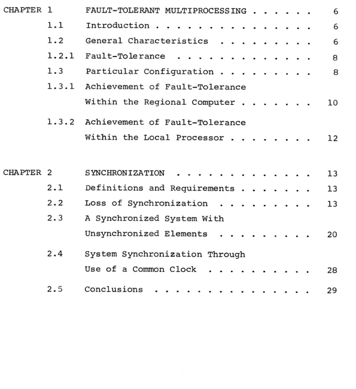
The essential elements of a multiprocessor are two or
more processors capable of simultaneously executing different programs (or the same programs) and a common memory accessible by all processors. This collection of units has a single path for input-output communication. A conceptual diagram is shown in Fig. 1.1.
Because of the parallel operation of the individual processors there is a significant increase in computational capability. This parallelism lends itself very well to the requirement of simultaneous control of many loops. The germ
0 0
M: MEMORY
I/O P: PROCESSOR
I/O: I/O CONTROLLER
of increased reliability is also inherent within the multi-processing concept: processors are alike and hence any proces-sor is capable of performing within any control loop at a
given time; it is this modularity which is the fundamental idea behind fault-tolerant multiprocessing.
1.2.1 Fault-Tolerance
In general, fault-tolerance is achieved through coded redundancy, replicated redundancy, or a combination of the two. Except in special instances, redundancy by replication is more
reliable and more simply implemented (Ref. 1). Within the
multiprocessor under study, fault-tolerance is achieved through comparison and/or voting amongst replicated units. Some basic assumptions in the design of this system are: (1) failures are independent of one another; (2) the same error will not be made at the same time by two elements which are in a
compari-son or voting scheme; and (3) multiple errors will not occur so as to outwit the fault-tolerant scheme (roughly equivalent to saying that errors will be separated by some minimum time). In a system which operates such that failures are independent of one another, the probability of assumptions nos. 2 and 3 being violated is extremely small.
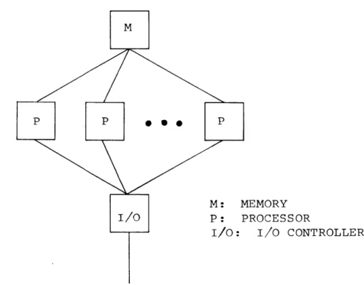
1.3 Particular Configuration
Figure 1.2 is a representation of the data management system recommended for the Space Shuttle. The system is designed to meet a fail operational, fail operational, fail safe (FOFOFS) specification; by this specification it is
meant that the system will maintain its performance capabili-ties after the occurrence of any two failures and, as a result
-- DISPLAY AND COMMAND SYSTEM - - - PRIMARY COV1UNICATION' SUBSYSTEM - - - AIR TRAF
FRDITER
NAVIGATIO\ A CONMROLLERS REFORMAT l ECM PE TR INPUT DEV DEVICES RCES M O
(INTERNALLY * EDI CATEDI11 A SIGNAL PROCFS50R MODULATION UNIT* ATC VOICE AN.D NAVAID M
REDUNDANT) I
-EMORY_
NOENGILE REGIONAL DATA BUS
MIDSHIP AREA
PAYLOADDOCKING SENSORS AND
OTHER PAYLOAD
SYSTEMS REGIONAL DATA BUS
DIAL
RE ENC UNATO iT
INERTIAL NTIZED BENON
POTING MODE
RFRNE ISENSORS SENSORS HYDRAULIC
ACTUATORS WHEELSAER
SURFACESI
AIC C0 TROL
RADAR AIR ATTA ALT. INTERFACE
ODULATION PO".ER RCSPOPELLA\NT
GENERATION CONDITIONI\G
MANAGANNC ENVIRONMIENTAI POlJER .1 CONTROLI - 1 DSRIB ,1 RS-
-CRYOGENIC ENVIRONMENTA POWER #2
MANAGEMEN1 CONTROL #2 DISTRI B
HYDRAULIC CRYOGENIC ENVIRONMENTAL POWER#3
ACTUATORS MANAGEMENT CONT RLL3DISTRIB RCSU#
WHEELS, E
TAILAREA BR PROPL
INTERFACEIOSSTEM ACT IRA RS CRYOG4 ANAGEMEN ENVIRONMENTAL POWER#4CONTROL #4 DISTRIB RCS#
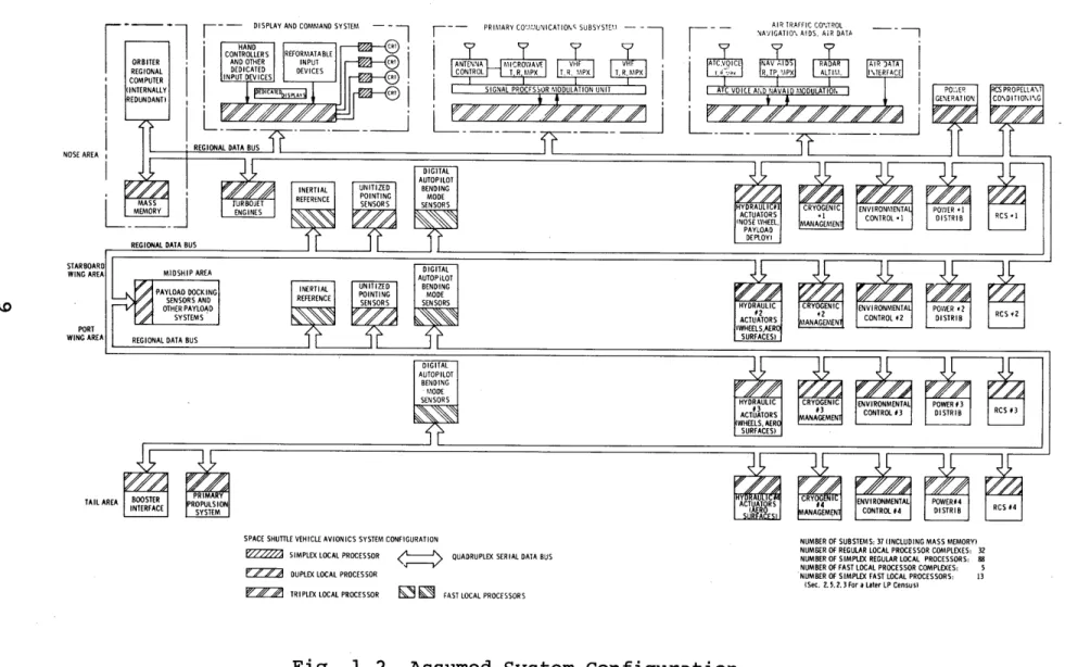
SPACE SHUTTLE VEHICLE AVIONICS SYSTEM CONFIGURATION
SIMPLEX LOCAL PROCESSOR QUADRUPLEX SERIAL DATA BUS DUPLEX LOCAL PROCESSOR
TRIPLEX LOCAL PROCESSOR
NUMBER OF SUBSTEMS: 37 INCLUDING MASS MEMORY)
NUMBER OF REGULAR LOCAL PROCESSOR COMPLEXES 32 NUMBER OF SIMPLEX REGULAR LOCAL PROCESSORS: 8B
NUMBER OF FAST LOCAL PROCESSOR COMPLEXES: S
NUMBER OF SIMPLEX FAST LOCAL PROCESSORS: 13
ISec. 25.2.3 For a Later LP Census)
FAST LOCAL PROCESSORS
Fig. 1.2 Assumed System Configuration
NOSE AREA STAR BOAR WING ARE PORT WINO AREA DIGITAL AUTOPILOT BENDING MODEl SENSOR S c A A
of a third failure, in the worst case, suffer a graceful degra-dation to a configuration which can still assure safe control of the vehicle. The system is hierarchical. The many sensors and effectors compose the lowest level. Next up in the hier-archy, the local processors transform between the serial-multi-plex format of the data bus and the sensor-effector formats;
also they are charged with the function of assuming those
burdens which would unnecessarily overload the top level of the system. At the top, the regional computer provides data proces-sing services to the entire system and manages interactions
between subsystems.
The use of multiprocessing techniques in the regional computer (RC) serves both to achieve fault-tolerance and to yield a larger throughput than would be possible with a simplex machine. Within the local processor (LP) duplication of
processors is used solely as a tool for the achievement of fault-tolerance.
1.3.1 Achievement of Fault-Tolerance Within The Regional Computer
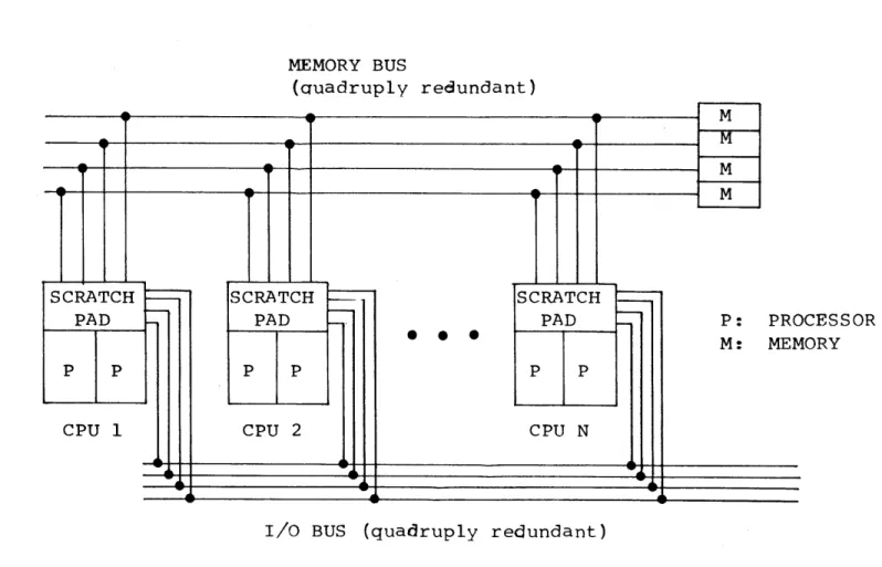
The regional computer multiprocessor configuration recommended by the Draper Lab is shown in Fig. 1.3. Each
Central Processing Unit (CPU) consists of two processors and a triplicated scratchpad memory which stores local temporary data and performs input/output (I/0) buffering. The memory, memory bus, and data bus are each redundant. The memory may be
-accessed by only one CPU at a time, and only one CPU (or LP) may be transmitting on the data bus at any time.
MEMORY BUS
(auadruply redundant)
P: PROCESSOR M: MEMORY
I/O BUS (quadruply redundant)
CPU error detection is achieved by comparing the outputs of the two processors, which run identical programs. The
detection of a CPU error triggers Single Instruction Restart (SIR), which consists of the moving of the scratchpad contents of the "failed" unit into memory and the subsequent loading of this information into the next available "healthy" CPU, where-upon the failed job is resumed. The recovery is transparent to
the software.
Fault-tolerance requirements are met by providing sufficient CPUs such that after an established number have failed the remainder can provide the necessary response speed and throughput to meet the system requirements. Thus, there is the advantage of extra processing capability before any CPU fails.
1.3.2 Achievement of Fault-Tolerance Within
The Local Processor
Depending upon system requirements a local processor may be simplex, duplex, or triplex. In any case error detection is
achieved as in a CPU: each LP unit contains two processors
which perform identical operations and compare outputs. Fault-tolerance is not through a restart mechanism, however. In the case of a duplex or triplex LP, local fault-tolerance is
achieved by keeping two LP units in synchronism. One feeds the data bus and the other has its output blocked; in the event of a failure of an LP unit, its output is blocked and the other's
is enabled. It is because of the differences amongst local processors serving different sensor-effector systems as well as a desire to limit data bus use that this mechanism for
CHAPTER 2
SYNCHRONIZATION
2.1 Definitions and Requirements
If fault-tolerance is to be achieved through comparison and/or voting amongst replicated units then there are two
requirements of operation which establish a need for synchro-nization. Obviously in order for the comparison to be
effect-ive, corresponding output information from each unit must be compared. Second, in order to assure equality of internal operations, accessed input information must be equal at cor-responding program points. It should be noted that although synchronization is required, simultaneous production of cor-responding information or simultaneous performance of cor-responding internal operations are not required. It is best to discard the notion that two events can be made to occur at the same time; in a real system there must always be finite tolerances in the "simultaneous" initiation of events. It is
fortunate that the synchronization requirements do not call for simultaneity, but, as shall be seen in Section 2.2, the
impossibility of assuring simultaneity gives rise to difficult-ies in assuring synchronization.
2.2 Loss of Synchronization
Assuming that several modules have been synchronized, loss of synchronization may be caused by a slivering of pulses.
A sliver can occur when two independent observers strobe a common signal while it is undergoing a transition. Because of gate thresholds and propagation delays, the observers may see different values of the signal. Slivering can cause differences
in the sequences of internal operations (leading to uncorre-lated outputs) or in the outputs of replicated comparators.
If the input or the event being strobed is phase-locked (i.e., dependent on the same clock) with the strobe, then
slivering may be avoided (barring the event of a failure) through good design techniques. If, however, the observed signal is produced asynchronously, or more generally, if the production of the observed signal is uncorrelated with the strobe or the call for data, then anti-sliver circuits must be utilized as necessary.
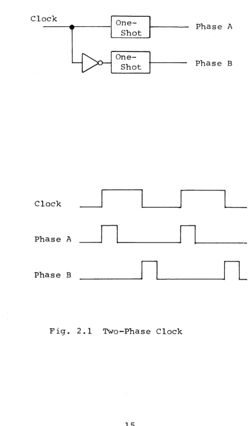
Current designs for anti-sliver circuits require the presence of a two-phase clock. A two-phase clock may be simply produced as illustrated in Fig. 2.1. The pulses of the two phases are mutually exclusive. The application of this clock to an anti-sliver circuit is illustrated in Fig. 2.2. The event pulse is stored in the first buffer; as illustrated,
either the concurrent (as in Case 1) or the next (as in Case 2) phase A pulse will cause the event to be stored in the second buffer, which is strobed, after settling, by a phase B pulse, thereby feeding a healthy signal to both units.
In a fault-tolerant system, when a replicated group of modules is receiving replicated information asynchronously, an anti-sliver unanimity circuit may be used to maintain synchro-nization. Such a circuit is illustrated in Fig. 2.3. The transmitted information from the A.s to the B.s is sliver-free
Clock One-Phase A Shot O Shot Phase B Clock Phase A Phase B
Event Pulse Phase A Phase B Case 1 - To Unit 1 - To Un it 2 Case 2 Event FF A Phase A FF B Phase B Outputs
Fig. 2.2 Anti-Sliver Circuit . .... ... ...
... ... ... IIIIIIr
..
.
...
...
..
.
...
Error Signals EjE.2. E3 A'3 --A'3 1l C1 A'12 A'3 Maj(Ap) = Com(A iM) AjA'2 v A'A' = A'iA'2A'3M L ---.. --- 4
Fig. 2.3 Anti-Sliver Unanimity Circuit
A1 A2 A3 Phase B v A'2A3 I I
and all the B. s receive synchronized information from all the A. s at the same time so that an accurate vote may be taken, and so that the B.s remain in synchronism. Each unanimity circuit waits long enough to accumulate all the A . s but not so long as to impair operation due to a failure of one of the A. s.
The timing chart in Fig. 2.4 illustrates a possible
sequence of events for the case of no failure. The event to be transmitted to the B. s is A. -+ 1. The example shown in Fig.
1 1
2.4 indicates that the events, A. -- 1, occurs first in A 2, 12
second in A1 , and last in A . Each event, A . -+ 1, is held in 31
the corresponding flip-flop, FFA. . Concurrent with the first Phase-A pulse shown, only FFA and FFA2 are at logic-level-l;
the flip-flops A{ and A are set during the first Phase-A pulse. The setting of the flip-flop A occurs during the
second Phase-A pulse. As can be seen in Fig. 2.3, each flip-flop A! is fed to each of the majority and comparator elements; the output of Maj(A.) is logic-1 when a majority of the inputs is at logic-1, and the output of Comp(A .M) is logic-1 only when all the inputs are at logic-l. In this example, Maj(A . ) -> 1 shortly after the first Phase-A pulse, while Comp(A .M) does not go to logic-1 until the occurrence of the second Phase-A pulse. The occurrence of Maj(A . ) -+ 1: causes the counter of Phase-B pulses to be reset to zero, causes the flip-flop FFM. to be set at logic-1, and also feeds the delay element A. The occurrence of Comp(A.M) -+ 1: causes FFM. to be reset (here, before the counter reaches an all-l's state, preventing the propagation of an error signal), and causes an output signal
Al A 2 A 3 FF A1 FF A2 FF A3 Phase A All A'2 A' 3 Ma j (A i) Com (A , M) Phase B Outi Errori
Fig. 2.4 Response of an anti-sliver unanimity circuit in the event of no failure
Fig. 2.5 illustrates a possible sequence for the case of a failure of one of the A s. Here A is described as having
failed to produce a bit of information (pulse). A is shown to precede A2 such that the events are passed on to the majority
and comparator elements separated by one Phase-A period. When flip-flop A goes to logic-1, A has already been set, and the majority elements go to logic-1, the comparator elements, how-ever, remain at logic-0, as flip-flop A was not set. Again, as a result of Maj(A.) -4 1, the counter is reset, FFM. is set, and the delay element is fed. It should be noted that the time-delay element, A, is used in order to prevent the false indication of an error when an all-l's state is indicated by the counter just prior to reset. The delay time required is dependent on clock frequency and propagation delay between a reset command and a response (assuming the counter was in an all-l's state) at the input of the error-indicating AND gate. In the example shown in Fig. 2.5 it is assumed that a 2-bit counter is used; hence, shortly after the occurrence of the third Phase-B pulse, succeeding the transition Maj(A.) -* 1, each line indicates both an output signal and an error.
2.3 A Synchronized System With Unsynchronized Elements
Before considering a multi-layered hierarchial system, it is wise to look at a simple model of this problem. Consider two modules each with one input line and one output line, each receiving and transmitting data serially. At an arbitrary time (t = 0), there is no signal on any line and the internal states of the modules (processors) are equivalent. For all time, t > 0, equivalent input data is received in serial bytes
Al A 2 A 3 FF Al FF A2 FF A3 Phase A' 1 A' 2 A' 3 A Maj (Ai) i Com(A ,M) Phase B Outi Error
Fig. 2.5 Response of an anti-sliver unanimity
circuit in the event of a failure of one of the Ais L ... ...
by both modules (not simultaneously); it is desired that the modules perform identical operations with identical internal and input data, and that corresponding bits of outputted data be recognized in order to facilitate comparison. In this
analysis it is not necessary to consider whether the processors are clock-driven (synchronous) or asynchronous machines; in either case, corresponding produced data bits are separated in time.
Not only may input data be received at different times by the modules, but more significantly it may be received at different points in the program being run by the two modules.
In the worst case such a condition may cause calculations to be made with different numbers, or a branch to occur in one processor but not in the other.
Two theorems, which taken together contend that two independent processors (or, in general, modules) may be synchronized, are stated and proved below.
Theorem 1. Two independent modules can be made to
perform identical operations with identical internal and input data.
Proof. Assume there is an interfacing unit associated with each module's input. The interfacing units may
communi-cate with each other as well as with their associated modules
-see Fig. 2.6. As in the case of the modules, the structure and operation of the interfaces are identical with each other. Assume that incoming bytes of information are buffered in
corresponding registers within each interface. Let each register have two extra bits (n extra bits - in the case of n parallel modules) above the number used to store input data;
Aout
Fig. 2.6
So -F Bout
,IBi Module B
these bits are used as check bits: a 1 in, say, the left bit will be taken to mean that the input byte to "me" has been stored in this register, and a 1 in the other bit will mean that the corresponding input byte to the other module has been stored in the corresponding register. Hence each module may be aware if corresponding information is available to both. The precise nature of the structure, possible microprogram, or requirements for fault-tolerance, of the interface units need not be considered presently. Rather the purpose of this
discussion is to determine, first, if a system meeting the requirements (stated earlier in this section) is possible.
Through use of these check bits by the program the modules may be kept in synchronization. Note that it is important that
updating of memory associated with a module by input data be controlled by the program so as to assure equality of available information at corresponding program points. Anti-slivering circuits will not be needed between interface and module as the structure of the programming will exclude slivering difficulties.
Theorem 2. Corresponding bits of output data produced by two independent modules can be recognized.
Proof. For purposes of buffering of information and comparison allow an interface unit to be associated with each module's output. To allow comparison these interfaces have
communication with each other. See Fig. 2.7. At an arbitrary t = 0, the registers of the output buffers are clear and no output bytes of information are stored in the registers of the
interface. When corresponding registers have been written into, the contents are compared by comparators within both
Aout
Bin -oi Bout
-OIFBi.4 Module B IFB0,
interface units. If there is no error the data is released to output and the registers read are cleared.
In order to determine how much buffering space is required consideration must be given to such things as: peak rate of output production, maximum time separation in product-ion of corresponding informatproduct-ion; and rate of comparsproduct-ion and clearing of registers within the interface units. If we define the following quantities:
p: peak rate of production (in bits/sec), n: length of one register (in bits),
t c: time required for comparison and subsequent outputting and clearing of register (in sec.), t s: maximum time separation in production of
corresponding bits, and
x: the number of registers required for one output interfacing buffer,
then if t n bits c p bits/sec
_1
x n (pt + 2n)
If the nature of the processor is such that it produces infor-mation in serial bytes, then the peak rate of production of bits, averaged over several bytes, will be less than p. If we define:
a: peak time averaged rate of production (in bits/sec.), and
then if n bits < n bits p bits/sec c a bits/sec at at pt x= a --- 1 l a s +F- 22 n t p n c _n bits
In the worst case t , then: c a bits/sec.'
at ata a p
pt
x =n (1 - -) + + 2
np n
A numerical example would be helpful; consider: p = 10 bits/sec, n = 16 bits, -3 t = 10 sec, s6 a = 10 bits/sec, ta = 1 sec, n then, if t
<
c p pts x = + 2 = 627 registers; n but if n< t<
n p c a at pt x - a (1 - -) s + 2 = 56,877. n p nIt can be seen that if the time required to ready a full register for the next load, t , is greater than the time it
c
n
takes the processor to fill a register, - , then the buffering
n
requirements are large. If t is larger than -, then the
c a
assure successful operation of the interfacing system.
The elements of design of this elementary system may be applied to a multi-layered hierarchical system. The primary drawback is in the requirements which must be imposed on the software of each processor in order to maintain synchronism of operations amongst replicated units. Different software
"tricks" will be required for different input information usage; any requirement imposed on software for purposes of maintaining synchronism will serve to decrease processor
speed and hence overall system speed. It is generally poor design procedure to depend on software improvisation for
system operation.
2.4 System Synchronization Through Use Of A Common Clock
Consideration is now given to a system in which all units are synchronous machines and one clock is used for the driving of all units. Replicated units which are driven by the same clock may be defined to be in synchronism in the case of units which, for purposes of fault tolerance, run the same program and receive the same data (the input being controlled by the same clock), the initiation of each corresponding
microprogram step as well as the receipt of corresponding bits of information occur concurrently (plus or minus some small tolerance); such units are said to be in tight synchronism.
First consider the same elementary problem explored in Section 2.3: the synchronization of two processing units. Even though corresponding input information and corresponding program steps are synchronized by the same clock, slivering
may allow one unit to recognize an input a microstep before the other. However, to maintain tight synchronism anti-sliver circuits are not necessary; two-phase clocking is sufficient to avoid slivering: one phase (A) is used for receiving and transmitting of information and the other phase (B) for driving the processor. Output bits produced by phase A are buffered and then compared and transmitted by phase B.
In a multi-level hierarchical system, such as the C.S. Draper Laboratory Space Shuttle Guidance Computer pro-posal, this method of synchronization should be adequate for
the entire system. However, information transmitted from sensor to local processor is not likely to be synchronized with the system clock; for such an interface anti-sliver
circuits (or anti-sliver unanimity circuits where called for by fault tolerance requirements) can provide the necessary
synchronization of receipt of information by local processors.
2.5 Conclusions
At first glance the system described in Section 2.4 is quite simple and desirable, especially in light of the alter-native (Section 2.3). The difficulty in the design of a system synchronized through use of a common clock lies in the design of the clock. Such a clock must meet the fault-tolerant
speci-fications both in its internal structure and in its distri-bution around the system; this is no easy task. Nevertheless
it is felt that it is much more desirable to add to the com-plexity of hardware design by calling for a fault-tolerant clock
than it is to suffer the pains of dependency on software impro-visation required in an unsynchronized system. It should also be noted that although a synchronous process is generally slower
than an asynchronous processor, an asynchronous fault-tolerant multiprocessor, due to increased software requirements and
necessary stop and wait periods, would probably be slower than a fault-tolerant multiprocessor driven by a fault-tolerant clock.
CHAPTER 3 CLOCKING
3.1 Specifications of a Fault-Tolerant Clock
As stated in Section 2.5, if a common clock is to be used to drive the system, it must meet the fault-tolerance specifications of the overall system. Whether the system specification be fail operational or fail safe, the clock
specification must be fail operational; the clock is as funda-mental to the system as the power supply. In the case of a
fault-tolerant clock designed to drive a Space Shuttle guidance computer, the clock would need to be able to perform after the occurrence of any combination of three independent failures.
Of prime importance in the design is that the synchro-nized state of the system is affected neither by any mode of
failure of the clock nor by the method of recovery from the failed state (i.e., the synchronization of the system must be transparent to clock failures).
For purposes of design and discussion, the distribution of the clock to all parts of the system will be considered as
a part of the clock design; this seems logical, as different concepts of fault-tolerant clocking may conceivably warrant different methods of distribution. It should be realized, however, that one of the keys to a good design will be mini-mization of the number of wires required for distribution. In
between modules may be on the order of 100 feet; in such a geographically distributed system wiring may assume a large share of the cost and complexity.
As a fault-tolerant computing system may have on the order of hundreds of modules, it is desired to minimize the logic required within each to convert the distributed clock information into the one train of clock pulses which is used for driving the module. Any failure of this logic will be considered as a failure of the entire module, which will be detected by comparison of outputs amongst replicated units.
3.2 General Methods of Design
Two general design approaches come to mind: (1) use a single clock in conjunction with a single-wire bus for distri-bution until the occurrence of a failure in the oscillator or
in the distribution, at which time another clock and its associated bus are brought into action; this principle is illustrated in Fig. 3.1; the enable circuits permit only one clock to be distributed at a time; (Enable)n passes clock n if and only if failure detectors 1 through n-i indicate failure
(initially clock 1 is distributed); (2) use a group of mutually synchronized oscillators which can tolerate the required number of failures and still have several "good" outputs; see Fig. 3.2.
3.3 Fault-Tolerant Clocking Through Failure-Detection and Subsequent Clock Substitution
In this section, through logical development, an explor-ation is made of the feasibility of a clocking system which
Clock 1 E
-*
I
|
e
Ei: (Enable)i
FDi: (Failure Detector)
Fig. 3.1 Fault-Tolerant Clocking through
Fig. 3.2 Fault-Tolerant Clocking through Synchronization of Oscillators
clock substitution. Consider Fig. 3.3; the clock system and the clock bus are to be designed to be fault-tolerant; neither the connection between module and bus, nor the module trans-ducer need be fault-tolerant, as a failure there may be
con-sidered to be a failure of the associated module. The design of the module transducer and its connections to the bus, how-ever, is an integral part of the design of the clocking system;
the module transducer converts the information on the bus into a single continuous clock waveform and needs to be designed such that the outputs of all module transducers are in synchro-nism. It will be seen that some elements of the clocking
system need to be external to the module, while others need to be associated with the module.
In order to simplify the feasibility study, system design for single-fault-tolerance will be explored first. Figure 3.4 is a general description of a single-fault-tolerant clock. In order to assure that each module utilizes the same clock,
failure detection should be external to the module.
The most obvious difficulty in designing the failure-detection and reconfiguration scheme is maintenance of synchro-nization through the failure and reconfiguration process. In order to prevent the failed clock from feeding the data manage-ment system, the clock waveform must be tested for failure
before it is used; but in order to detect failures in distri-bution, the clock waveform must be tested after distribution.
it would appear that each module transducer must be designed to "hold" (delay) use of the clock waveform until it is sure that a failure has not occurred. When a failure is detected each transducer holds its output at, say, logic-level-O, until after the clock system has been reconfigured and a "good" clock
Lock
*
-clock
ystem
bus 0bus r.------Module
Transducer
Module
F
E: Enable
FD: Failure Detector
waveform is available, at which time each transducer passes the good clock waveform. The difficulty now is in assuring that
synchronization is maintained through the local transducer process of: output-hold-output.
If one of the enable circuits fails such as to produce a random output, the module transducer is required to choose the "good" waveform, if single-fault-tolerance is to exist. The amount of circuitry required for the transducer to choose the "good" waveform can be reduced if the state of the failure detector is made available to the transducers (via a failure detector bus); if this is done, the enable circuits shown in Fig. 3.4 become superfluous. Figure 3.4 may be revised as illustrated in Fig. 3.5. The failure detector may be simply implemented as illustrated in Fig. 3.6. The circuit is
designed to allow a tolerance on clock pulse width and separ-ation between pulses; if the tolerance is violated the output of the failure-detector goes to, and is held at, logic-1; the
reset capability is provided for initializing the clocking
system. The pulse widths of the one-shot outputs determine the tolerance; it is a straightforward procedure to determine the necessary one-shot timing, given: clock frequency, duty-cycle, and allowed variations in both, as well as data concerning
tolerances, of the propagation delays andone-shot pulse widths,
associated with the failure-detector components. The retrig-gerable one-shot should have an output pulse width of approxi-mately twice the period of the clock; it assures the detection of a failure to logic-level-O or logic-level-1.
Figure 3.7 is the design of a module transducer which may be used in conjunction with the clock system of Figures 3.5
reset
(bus) 1
failure detector bus
Clock 2 (bus) 2
Fig. 3.5 Revised Single-Fault-Tolerant Concept
---clock
reset
Fig. 3.6 Failure Detector
T
bus---
alO.S
-1
F O.S-2 F1 10.S -3 FA3
Out
Module TransducerFig. 3.7 Module Transducer for Single-Fault-Tolerant
it allows the prevention of the propagation of a failed clock. In a system state prior to clock failure, the waveform of clock 1 is passed through delay, A1, and one-shot, o.s.1 , and then to
the output. If a failure is indicated, FF1 - 1, causing the termination of the distribution of clock 1 and the subsequent distribution of clock 2 to each module. Additional circuitry is provided in each transducer for maintenance of synchronization during and after the switching period. Slivering within the transducer in effecting the cut-off of clock 1 and the cut-in of clock 2 may, in some cases, yield an extra pulse associated with clock 1 or an extra pulse associated with clock 2; thus after the switching has taken place the total number of clock pulses supplied to each module may differ by one or two. If an
"extra" pulse of clock 1 is propagated, FF2 is set, and if an "extra" pulse of clock 2 is propagated, FF3 is set. In those transducers in which FF2 or FF3 was not set during the switch-ing process, one extra pulse for each unset flip-flop is insert-ed between the end of the clock 1 waveform and the beginning of the clock 2 waveform, thereby maintaining synchronism. Require-ments are established for values of A1, A2, 3, A4, and the
pulse widths of the one-shots, as well as their tolerances; the requirements are imposed by the system parameters (e.g., clock frequency), as well as by the required method of operation.
It is believed that the module transducer shown in Fig. 3.7 is an example of a minimally complex (or nearly so) trans-ducer required for fault-tolerant clocking through failure detection and subsequent clock substitution. The necessity of requiring such complex operations to be performed on the module
level, rather than the external clock system level, has been justified in the development of this section. Because of the
module-level complexity here, it is felt that designs such as described in later sections of this thesis, are much more
desirable; hence a detailed analysis of the module transducer illustrated in Fig. 3.7 is not presented.
For n-fault-tolerance, the system becomes more compli-cated on all levels, and, of course, it is the increased com-plication on the module level which is particularly undesirable.
It is concluded that fault-tolerant clocking through failure detection and subsequent clock substitution is possible, but is extremely costly in hardware implementation.
3.4 The McKenna Clock 3.4.1 First Concept
In August, 1971, William Daly and John F. McKenna, in a C.S. Draper Laboratory memo (Ref. 2), described their design of a fault-tolerant clock. Figure 3.8 illustrates the concept proposed for single-fault-tolerance. It is seen that this
design conforms to the method of clocking shown in Fig. 3.2 and indeed may be described as a synchronization of oscillators. It should be noted, however, that here a single clock element, apart from the others, is not an oscillator. Rather, as shall be seen in the analysis to follow, each clock element depends
on the occurrence of the transition in state of several of the clocks in order to be driven to change its own state.
n
The quorum function Q is defined to be 1 if at least a a
of the n independent variables C1, C2, ''' n are 1, and 0
otherwise. For example: 4
6 C1 Cl C2 C3 C4 (A Cl r- -C2 C3 C4 ---- - - - ---C2 --- C C2 C3 C4 L---Cl ---C2 C3 C4 F
---Fig. 3.8 Daly-McKenna Clock
, *
C3
C4
tf Ia * S t ,
Q2
=
CC
2+
CC
3+ C
1C
+
C
2C
3+24
+ C3C
4 Q3 CC2C3 1 + CC42C4+ CC43C = C2C3C4
Q = C C2C3C4
1
23
4
4
4
Q and Q may each be realized through two levels of Boolean
2
3
gating or through one level of threshold logic. The use of threshold logic, however, offers
no advantage unless LSI threshold logic technology is to be used. All clock lines are distributed to each synchronous
module within the system. It will be demonstrated in a later part of this section that majority voting and subsequent filter-ing within each module is necessary to maintain system synchro-nization, and an adequate module transducer will be described.
The logic required to induce free-running oscillation after power-on is not shown in Fig. 3.8. For the purposes of this analysis it will be assumed that the clock elements are already oscillating in synchronism at the time of observation. Timing analyses will be made, to demonstrate system performance.
For purposes of analysis the following assumptions are made: each gate has a propagation delay equal to A; the propa-gation delay in forming a quorum function is 2A; At is a pure delay, greater than or equal to 8A (in order to avoid slivering within the clock element which could yield spikes in the output, At must be greater than the propagation delay through the
series of gates: H21, A31 M2 1, N 4 1, which is 4A; however,
since by most manufacturers' specifications propagation delay within a simple Boolean gate may reach to nearly twice the
typical delay time, in the worst case the delay through four gates in series may approach 8A.
Assume that the clock elements are oscillating in synchro-nism. Assume that at time: t=t1 , C1 goes to logic-i; t=t2'
C2 -> 1; t=t 3 C 3- 1; and at t=t , C4 -> 1 (see Fig. 3.9), where
t > t3 > t2 > t . Assume that at an initial time of observation,
(t1 - eE), all propagation, within each clock element, caused by
the previous transition, C.-+ 0, has ceased (this will be veri-fied within the analysis to follow); therefore the outputs of the gates (Ref. Fig. 3.8) are as follows:
Initially: C. = 0 4 4 D 0; Q 2.=0 21 31 Dii 0; D .= 0 H 1; H 1 i li A 2 0; M =0 A .= 1; A .i 0; M 2i 0 A .1 0; A .= 0; M .= 1 A .= 0; A .i 0; M .i 1 N . 1; N .4 = 1 N =C =0 2i ~
i
N .= 1 3iGiven the initial state and the assumed progression of events, the timing analysis is as follows: for reference
purposes all transitions are numbered.
C
i
C 2 C3 C4i
-3. t 2 t 3t 4 t4 4
Q . and Q . remain at 0
2i
3i
.*. gate X ., i = 2,3,4, remain unchanged from the initial state
N 3l +0 at t 1+ A (the validity of this statement is dependent on the nature of transition (3.1)) (3.2)
C2-+1 at t2 (N 22- 1) (3.3) 4 Q .- 1 at t + 2A (3.4) 21 2 4 Q . remains at 0 3i N 32 0 at t2 + A (as in (3.2)) (3.5) A . 1 at t + 3A (3.6)
21
2
D .- +1 at t + 2A + At (3.7)li
2
H .-+ 0 at t + 3A + At (3.8)li
2
A .- 0 at t + 4A + At (3.9)li
2
It has already been assumed that At > 8A, but it is still interesting to note that for At = 0, a short duration pulse
might or might not be generated by M 1., yielding possible
slivering within the clock's logic and hence unpredictable operation. C 3 1 at t3 (N23 -+ 1) (3.10) N 33- 0 at t3 + A (as in (3.2)) (3.11) 4 Q . remains at 1 2i D . remains at 1 li 4 Q 4. 1 at t + 2A (3.12) 31 3 H .- 0 at t + 3A (3.13) 2i 3
A . 0 31i M .- l 2i1 N 4 0 D .i 1 2i A .i 1 M .- 0
4i
31' N 3i= (N2i N 4i 1 A 4i 1 4' M . 0 2i A8i 0 4' As a result of Q 4.-4 0 21 Q 4.-+ 0 31 A .4Q0 2i M ii 1 N .i 0 li D .i 0 li li A i-+ 1 at t 3+ 3 at t 3 + 3 at t 3 + at t 3+3 at t 3 + at t 3 + at t 3 + C i) > 0 at t 3 + at t + 3 at t + 3 at t3 + at t + 3 (3. 21) : at t + 3 at t + 3 at t 3+ 3 at t + 3 at t + 3 at t + 3 at t + 3 at t3 + 4A 5A 6A2A
+ At3A
+ At4A
+ At5A
+ At at t3 + 6A A At5A
+ At 6A + At 7A + At 8A + At 9A + At 8A + At 8A + At9A
+ At 10A + At 11A + At 8A + 2At9A
+ 2At 10A + 2At (3.14) (3.15) (3.16) (3.17) (3.18) (3.19) (3.20) (3.21) (3.22) (3.23) (3.24) (3.25) (3.26) (3.27) (3.28) (3.29) (3.30) (3.31) (3.32) (3.33) (3.34)M -> 0 at t +
31
3
11A + 2At(N . = C.) - 1 att + 12A + 2At
2i 1 3 N .i 0 at t + 31 3 N .-l at t 3+ li 3 A .5il at t + li 3 M -> at t3 + A . 0 at t + 5i 3 M .
1
at t 3+ 31 3 H .->1at t +21
3
A . l at t +3i
3
D .-> 0 at t +± 21 3 A .- 0at t +± 81 3 A .- 0at t +± 4i 3 13A + 2At 12A + 2At 13A + 2At 14A + 2At 15A + 2At 16A + 2At 9A + At 10A + At 8A + 2At 9A + 2At 9A + 2AtIt is seen that the last transition of each gate
(3.35) (3.36) (3.37) (3.38) (3.39) (3.40) (3.41) (3.42) (3.43) (3.44) (3.45) (3.46) (3.47) (up to
transition (3.47)) restores the gate to its initial setting. Because of transition (3.36), C.-> 0 at a time later: 6A + At; and because of C -> 0, C- 4 1 in another increment of time: 6A + At. The duty-cycle of C. is 50%. The period is:
T .
ci - 12A + 2At Hence the maximum frequency is:
f
1
max 28A
For medium speed TTL, A - 12 ns; therefore f ~ 3 MHz. max
At must be greater than 4A, for successful operation, may be demonstrated. Assume that A < At < 4A; then transition (3.17) occurs before (3.16) and a possible timing sequence is as follows:
D - 1 at t + 2A + At (3.48) 2i 3 N4 - 0 at t3 + 6A (3.49) A .-- 1 at t 3+ 3A + At (3.50) 41 3 A -4 1 at t3 + 3A + At (3.51) A 4i 4 0 at t 3 3 7A ++ (3.52) M 2i -+ 0 at t 3 + 4A + At (3.53) M .-4 41 0 at t 3 + 4A + At (3.54) M 2i 40 at t 3+ 3 8A (3.55) N 2i .i l at t 3 + 5A + At (3.56) N -+ 1 at t3 + 5A + At (3.57) A .-+ 0 at t + 5A + At (3.58) 8i 3 A Bi- 1 at t 3 + 9A (3.59) A -+ 1 at t + 6A + At (3.60) 4i 3 (N21 A C )-+ at t3 + 6 + At (3.61) M 4 .- 1 at t + 6A + At (3.62)
41
3
M -4 0 at t3 + 10A (3.63)Transitions (3.61) and (3.62) both occur at t3 + 6A + At, but if (3.62) occurs just before (3.61) the following transition
may occur in some clock elements:
N .-4 0 at t 3+ 7A + At (3.64)
31 3
So, it is seen that for A
<
At < 4A, proper operation can-not be assured.Now assume that At < A; then as a result of transition (3.12): D .i 1 at t + 2A + At (3.66)
2i
3
H . 0 at t + 3A (3.67)21
3
A - 1 at t + 3A + At (3.68)4i
3
A .i 0 at t + 4A (3.69)3i
3
Since (3.68) occurs before (3.69), M will not go to 1 and therefore C. will not go to 0, yielding a non-oscillatory con-dition.
It has been shown, in support of the original assertion, that At must be greater than 4A. Also, as mentioned, in order to assure operation in the event that gate propagation delays are nearly double nominal value, At should be no less than
8A
nom.
The principle of operation is seen to be as follows: when
4
4
Q -+ 1, C.-+ 0 6A + At later; when Q -> 0, C.-+ 1 6A + At later.
3 2 1
Differences amongst clock elements in the propagation of the
4
signal triggered by the leading edge of the Q pulse or in the propagation of the signal triggered by the trailing edge of the
4
Q pulse will cause minor time separations in occurrences of
2
leading and trailing edges amongst clock element pulses. It
4
should be noted that if for clock element 1, Q .- + 1 before
214
H -+ 1, then C. is driven to logic-1 5A after Q -> 1.
1i i 2
Similarly, if Q .-+ 0 before D .-4 1, then C. is driven to logic-0
431 2i 1
6A
after Q -4+ 0.For purposes of determining the effect of differences in propagation delays on clock performance consider the following definitions and analysis: first, assume that the delays of each clock element are within tolerances such that the
"set-to-4
4
agree" (Q4 - 1 drives C.-+ 1 or Q ->0 drives C.-+ 0) function is not
2 1 31
utilized in normal operation; now, define the time between the 4
event Q3 - 1 (here, Q refers to the conceptual quorum function, not the physical implementation) and the resulting event C.-+ 0
4
as (3t i define the time between the event Q -+ 0 and the
d i 4 2
resulting C.-+ 1 as (5t U) . Once the event Q -> 1 has occurred,
4
13
Q 2- 0 will occur (Et ) later, where x is the clock possessing
2 d x
4 4
the next to the largest (6td) ; after Q2 - 0 occurs, Q 3-+ 1 will occur (btU)y later, where y is the clock possessing the next to
the largest (Stu)*
Two specifications which considered together offer a signi-ficant measurement of clock performance, may be defined as
follows:
AT U duty-cycle of the function C C2 C3 C4 ATd duty-cycle of the function C C C3 C4'
These two specifications indicate, respectively, the size of the overlap region of the clock pulses and the size of the overlap region of the clock 0-states. If there were no differences amongst propagation delays of like elements then ATu and ATd
would both be I . Following is a derivation of the relationships
2
between AT , ATd and the (5tu)'s, (5td 's:
Assign numbers to the clocks such that:
Assign letters to the clocks such that:
(5t)
a
<
t)b<
(t
)
<(t )
(3.71)
There are 4' distinct sets of the four clock outputs, yet in each case:
the period of the clock is given by:
T = (td )3 + (6t )c (3.72) and
1
AT = - [ (8t ) -(5t ) + (5t .) ](3.73) u T d 1 u i d u c AT = -[ (t ) - (t ) + (Et ) ] (3.74) d T u a d 4 d 3Two cases are illustrated (Figs. 3.10, 3.11) for the purpose of shedding some light on why AT and AT are independent of the
u
d
manner of the pairings of the (5td) 's with the (5t u) 's in the four clocks.
The percentage variation of the (6td) 's and the (5t ) 's around some nominal value is dependent on both component speci-fications and component selection; testing and subsequent
selection of components will yield a minimum variation. A worst-case analysis will yield a direct correlation between clock
performance, as measured by ATu and ATd, and the tolerances of
the (8td) 's and (St ) 's. If (Ste) and (8td) fall within a range (6t) (1-x)
<
6t<
(6t) (1 +x), then from eqns (3.72), (3.73),nom nom and (3.74): 1-3x < 1 [A T ] = [A T
d]
(3.75) a ue m d m0, x i i(5tu)d - (btu)cl SQ 0
-
(Btd)3 4 Q+
(Stu) c T = (6~td)3 + (Stu)c ATu = I[(8td)1 - (&tu)d + (tu)lTU
ATd = [(Stula - (8td)4 + (Ftd)31
Fig. 3.10 Determination of ATu
C4
Clb
C2c
C3d
H(td)4- (8t3)31 t u d - ( tu c I Q4 0 Q4
Q
2-' 0
Q1
(8tdg-.I
8t
T = (8td) 3 + (8tu c .1 ATU = (8td)1 - (8tu)d + ATd =[(8tu)a - (8td) 4 + (8tul)c (8td)3JFig. 3.11 Determination of ATu
and ATd - Case 2 Cla
C3b
C 2c
to assume that [(6td)
3-
(td)
2]
or [(Ftd 4
-
(td) 2
1is larger
than 6A, or that
[
(t
.) c - (3t )b]
or [ (6t ) - (St)b]
is largerthan 5A, but that the above analysis is valid because, in the
worst case (6t ) and
(Ft )
may be equal to (bt)
(1-x) and,
u
a
d 1
nom.
the other (t d)
's and (t u)
's equal to (st)
(l+x); in this
d
u
nom.
worst case the set-to-agree function is not utilized.
By nature of the design of the clock, any single failure
can directly affect the output of only one clock element. In
order to examine the post-failure operation of the circuit it is
not necessary to examine the failure-modes of every logic gate;
rather it is sufficient to examine the effect on clock operation
of one failed clock element. The operation of the clock is
examined below for three modes of failure of any one clock
element: failed to logic-level-1, failed to logic-level-0, and
random oscillation. Flaws in the design of the clock will be
exposed, and a revised design will be recommended.
The following definitions will be useful in the analysis:
3
Q
=
1 if and only if n out of the three "good"
n
clock elements are at logic-level-l.
Using previously defined nomenclature, assign
numbers and letters to the three "good" clock
elements such that:
(Std
1
(1td
2(Std
3
(3t ) <
u a
tb
u
(t
uc
u c
)Denote
(8td)
and (Stu) of the failed clock element, prior
to failure,as (5td)f and (btu)fI respectively.
not fail as a result of the occurrence of the failure, then the
4
3
4
event
Q
4- 1 is equivalent to Q3 -1,
the event Q4 -0
is equivalent33
2
2
to Q
1- 0, and the principle of operation of the three good clocks
remains the same: once the event Q
-41, has occurred,
Q -
0 will
2
3
3
occur (5td 3 later; as a result of the event Q3-> 0, Q
21 will
occur (5t
b
later. Therefore the period of oscillation of each
good clock is:
T 1(3.76)
fl
(Std)3 + (St
)b
where the subscript fl denotes failure to logic-level-1. Unless
(3td)f > (5td)3 and (3tU)f
<
(t
)
b, the period prior to failure
differs from T
.
If the failure is to logic-level-0 and if the system does
not fail as a result of the occurrence of the failure, then the
4
3
4
event
Q
34- 1 is equivalent to
Q34
1, the event Q2- 0 is equivalent
3
3
3
to Q2 - 0, and: once Q