HAL Id: hal-00558472
https://hal.archives-ouvertes.fr/hal-00558472v3
Submitted on 2 Feb 2011
HAL is a multi-disciplinary open access
archive for the deposit and dissemination of
sci-entific research documents, whether they are
pub-lished or not. The documents may come from
teaching and research institutions in France or
abroad, or from public or private research centers.
L’archive ouverte pluridisciplinaire HAL, est
destinée au dépôt et à la diffusion de documents
scientifiques de niveau recherche, publiés ou non,
émanant des établissements d’enseignement et de
recherche français ou étrangers, des laboratoires
publics ou privés.
Novel E-beam lithography technique for in-situ junction
fabrication: the controlled undercut
Florent Lecocq, Cécile Naud, Ioan M. Pop, Zhihui Peng, Iulian Matei, Thierry
Crozes, Thierry Fournier, Wiebke Guichard, Olivier Buisson
To cite this version:
Florent Lecocq, Cécile Naud, Ioan M. Pop, Zhihui Peng, Iulian Matei, et al.. Novel E-beam
lithogra-phy technique for in-situ junction fabrication: the controlled undercut. Nanotechnology, Institute of
Physics, 2011, 22, pp.315302. �10.1088/0957-4484/22/31/315302�. �hal-00558472v3�
undercut
F. Lecocq, C. Naud, I. M. Pop, Z. H. Peng, I. Matei, T. Crozes, T. Fournier, W. Guichard and O. Buisson
Institut N´eel, CNRS and Universit´e Joseph Fourier, 38042 Grenoble, France
We present a novel shadow evaporation technique for the realization of junctions and capacitors. The design by E-beam lithography of strongly asymmetric undercuts on a bilayer resist enables in-situ fabrication of junctions and capacitors without the use of the well-known suspended bridge[1]. The absence of bridges increases the mechanical robustness of the resist mask as well as the accessible range of the junction size, from 10−2µm2 to more than 104µm2. We have fabricated Al/AlOx/Al
Josephson junctions, phase qubit and capacitors using a 100kV E-beam writer. Although this high voltage enables a precise control of the undercut, implementation using a conventional 20kV E-beam is also discussed. The phase qubit coherence times, extracted from spectroscopy resonance width, Rabi and Ramsey oscillations decay and energy relaxation measurements, are longer than the ones obtained in our previous samples realized by standard techniques. These results demonstrate the high quality of the junction obtained by the controlled undercut technique.
PACS numbers: 85.25.Cp, 81.16.Nd, 03.67.Lx
INTRODUCTION
On-chip metallic junctions are the building blocks for a wide variety of nanoelectronic devices such as sin-gle electron transistors [2], spin-based electronic devices [3, 4] and superconducting circuits such as SQUIDs [5], voltage standard circuits[6], RSFQ logic circuits[7], nano-fridges[8] and superconducting qubits [9]. The Shadow Evaporation Technique (ShET)[1] with a sus-pended bridge of resist appears as a very useful technique to realize these circuits. For ShET the two metal evap-orations, as well as the oxidation to obtain the tunnel barrier, are made without breaking the vacuum there-fore enabling high quality junctions. ShET is simple (one lithography step) and flexible (independent on the metal choice) and enables submicron size tunnel junctions. These performances make this technique often preferable compared to the Multi-Layers Technique (MLT)[10, 11]. However ShET presents important limitations due to the suspended bridge. Overcoming these limitations would open the way for designing new types of circuits. One of the ShET disadvantage is the fragility of the bridge which makes any etching by plasma difficult in order to clean the substrate surface before evaporation. In addition, the bridge prevents from an efficient cleaning of the junction surface before evaporation since it is located just above the junction. As a consequence the resist residues can contaminate the tunnel barrier and alter its oxide qual-ity. Moreover the mechanical strains on the suspended bridge make impossible the fabrication of large tunnel junctions (typically larger than 10µm2) and large
capac-itors.
In this paper we report on a Josephson junction phase qubit made by a novel technique using angle evapora-tions but without using suspended bridges. This tech-nique, called hereafter Controlled Undercut Technique (CUT), is based on the control of strongly asymmetric
undercuts in a bilayer resist. By adjusting the under-cut position and its depth, we select for each angle of evaporation whether the metal will be deposited onto the substrate or on the resist wall which will be removed af-ter lift-off. By this way we can control which wire will be connected to the junction. Using the CUT, we have fabricated a Camelback phase qubit based on a zero-current bias SQUID. Josephson junction zero-current-voltage (IV) and qubit coherence properties have been charac-terized and compared to our previous Camelback phase qubits made by Multi-Layers Technique (MLT)[12] and ShET techniques[13].
CONTROLLED UNDERCUT TECHNIQUE
The CUT was developed using a 200nm thick PMMA imaging layer on top of a 700nm thick copolymer PMMA/MAA support layer spun on a Si/SiO2 wafer.
An E-beam writer operating at 100kV draws two suc-cessive types of patterns. A first one using a high dose exposure defines the opened wires in the imaging layer. The second pattern using a low dose defines the under-cut in the support layer (Fig.1(a)). These two different patterns are possible because the PMMA sensitivity is around three times lower than the PMMA/MAA one. After development (MIBK(1):IPA(3) during 30s and rins-ing with pure IPA) we obtain a strongly asymmetric un-dercut (Fig.1(b)). Typically we achieve on one side a de-signed undercut with a depth up to more than 1µm while on the other side we observe an undesired residual under-cut smaller than 50nm. A light oxygen plasma RIE cleans the resist residues on the wafer. The next step consists of two evaporations with angle θ = −45◦and θ = +45◦,
separated by an in-situ oxidation (Fig.1(b)). The first evaporation produces a wire on the substrate whereas the second one is deposited on the resist wall. After
re-2
sist lift-off only one wire remains on the substrate. In the case of an undercut designed on the other side, the situa-tion is symmetrically reversed: the second evaporasitua-tion is deposited on the substrate and the first one on the resist and removed after lift-off. Therefore the CUT enables to design undercut patterns such that we select for each evaporation which connecting wire remains or not on the substrate. SiO2 (100nm) Si PMMA/MAA (700nm) High Dose Low Dose 2nd evaporation 1st evaporation Si (a) (b) et W d min q (c)
FIG. 1: Schematic cross sectional diagram of the CUT. (a) During the E-beam exposure. (b) During the evaporation af-ter the resist development. (c) A cross section SEM image before lift-off obtained by cleaving the Si wafer. The first evaporation wire is below the undercut. The second evapora-tion wire is on the resist wall.
Fig. 2(a) illustrates the typical resist mask design to realize a junction using the CUT. The central opened area defines the junction. The two opened lines, on both side of the central area, define the two wires connecting the junction to the external circuit. A 1µm deep under-cut is present on the right of the upper connecting wire and on the left of the lower connecting wire. A cross sec-tion of the upper wire corresponds to Fig.1(b) and (c). To realize a junction we perform two evaporations with opposite angles as mentioned previously. The first evap-oration, coming from the left in Fig. 2(a), only deposits on the substrate the bottom electrode of the junction and the upper wire. The evaporation of the lower wire is deposited on the resist wall. Similarly, the second evapo-ration, coming from the right, deposits on the substrate the top electrode of the junction, the lower wire on the substrate and the upper wire on the resist wall. Fig.2(b) shows the junction after lift-off. The two evaporations are shifted by about 1.6 µm because of the different an-gles.
The connecting wires must have a width W which sat-isfy the condition W < tg(θ) ∗ et− δmin where etis the
(a) (b)
1mm
JJ
upper wire
lower wire
FIG. 2: (color online) (a) SEM pictures of a junction (central part) and its two connecting wires before lift-off. The bright areas indicate the undercuts, the dark area the developped resist. The white dashed line and two arrows indicate the Fig1(c) cut. (b) SEM pictures after lift-off. The upper and lower wires which correspond respectively to the first and the second evaporation, connect the bottom and top electrode of the Al junction to the circuit. The alignement of the two Al connecting wires from the unaligned resist mask is realized because of the two opposite evaporation angles.
0 200 400 600 800 1000 0 200 400 600 800 1000
Designed undercut depth (nm)
Obtained undercut depth (nm)
20keV 100keV 1µm 1µm δ min,20kV δmin,100kV (a) (b)
FIG. 3: Obtained undercut depth after development versus designed undercut depth for electron beam energy of 20keV and 100keV . Insets a) and b) present SEM images of an asymmetry undercut, with the minimum achievable undercut depth δminon one side and a 1µm deep undercut on the other
side, for electron energy of 20keV and 100keV , respectively.
support layer thickness and δmin the residual undercut
depth (see Fig.1). Indeed if the width is too large, both angle evaporations will be deposited onto the substrate and will short-circuit the junction. This width is the key parameter to quantify the feasibility of the CUT. It in-creases with the resist thickness and linearly dein-creases with δmin.
In order to quantify the undercut control in our pro-cess, we have measured the obtained undercut depth af-ter development as a function of the designed one (see Fig.3). The data were obtained by measuring the under-cut depth before lift-off on each side of a 250nm large wire. For deep designed undercuts (above 300nm), the measured undercut corresponds to the designed one and a good undercut control is reached independently of the
E-beam voltage. For zero designed undercut, a residual undercut is observed which corresponds to δmin. It is
mainly produced by proximity effect and is strongly de-pendent on the E-beam voltage [14]. As shown in the insets in Fig.3, δmin drops from 250nm to 40nm when
the voltage increases from 20kV to 100kV. This effect shows the advantage of high voltage for the control of strongly assymmetric undercuts.
Therefore we have developed the CUT using a 100kV E-beam to minimize δmin and maximize W . Although
preliminary lithography at 20kV was unsuccessful, in-creasing the bottom resist thickness should make this new technique feasible even at this low voltage. We would also like to mention that a better undercut control can be achieved by using either another resist [15] or another de-velopper instead of MIBK [16, 17]. This would minimize the residual development of unexposed resist.
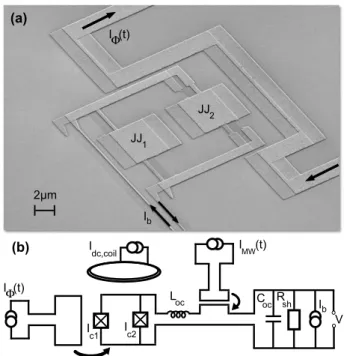
I (t) F I (t)MW I dc,coil I c1 I c2 L oc C ocR sh I b V (b) (a) I b I (t) F 2µm JJ 1 JJ 2
FIG. 4: (a) SEM image of a Camelback phase qubit based on a dc SQUID after lift-off.(b) The dc SQUID phase qubit is controlled by a dc bias current Iband flux Φb, manipulated by
a MW current and measured by a nanosecond flux pulse. The qubit is decoupled from the environment by a large kinetic inductance Le = 10nF and capacitance Ce = 200pF and is
shunted by a resistance Rsh= 20kΩ.
CAMELBACK PHASE QUBIT REALIZATION
A Camelback phase qubit has been fabricated using the CUT. Fig.4.a shows a SEM image of the device after lift-off. The SQUID loop with the two 10µm2-JJ (central
part) is connected by two 100 nm-thin and 200 µm-long current bias lines (visible on the left bottom side). The larger wire on the right side is the antenna for the high
frequency bias flux. Fig.4.b shows the electrical circuit for the measurement of the Camelback phase qubit.
The Al/AlOx/Al qubit tunnel junctions and the device
were formed by evaporating from a −45◦angle 15 nm of
Al in a high vaccum chamber, oxidizing for 10 min in 30 mbar of oxygen, depositing at a 45◦ angle 30 nm of Al,
and then lifting off the pattern. The IV characteristics at low temperature of the dc SQUID gives the normal re-sistance of the two parallel tunnel junctions, Rn=246 Ω.
The total critical current, Ic,1+Ic,2= 1.426µA, measured
at zero magnetic flux, is consistent with the Ambegaokar-Baratoff formula, π∆
2eRn=1.405µA where ∆ = 220µeV is
the Al superconducting gap extracted from IV charac-teristics. The subgap resistance is larger than the 20 kΩ of the shunt resistance and the retrapping current is less than 7 nA. Moreover the measurement of the Ic versus
flux shows a very small critical current asymmetry be-tween the two JJ of the SQUID, Ic,1− Ic,2 = 3nA. The
small values of the retrapping current and critical cur-rent asymmetry as well as the large subgap resistance is a first proof of the high quality of the JJ made by the CUT. 0.3 0.35 0.4 0.45 0.5 0.55 0.6 5.5 6 6.5 7 7.5 8 8.5 9 9.5 Φb/Φ0 Frequency [GHz] 9.48 9.5 9.52 9.54 0 0.05 0.1 Frequency [GHz] Pesc ∆ν 01=4.5 MHz 0 100 200 300 400 0 0.2 0.4 0.6 0.8 Pulse duration [ns] Pesc T 2,Rabi = 170 ns (a) (b)
FIG. 5: Camelback phase qubit dynamics. (a) Spectroscopy: Pesc versus reduced flux and microwave frequency for a
cur-rent bias Ib = 2nA. Pesc is enhanced when the frequency
matches ν01. Dark and bright gray scale correspond to high
and small Pesc. Dashed line is ν01 versus reduced flux
de-rived from the theory presented in Ref.[12]. Insets (a): Qubit spectroscopy at Φ/Φ0 = 0.308 and Ib= 2nA. In this
partic-ular frequency window TLS are not visible. The fit is made by lorentzian curve. Inset (b): Rabi oscillation at the same working point.
We present results on the quantum dynamics at zero current bias when the potential is quartic and the qubit is insensitive to current noise[12]. Spectroscopy mea-surements were performed by applying a current-bias mi-crowave pulse of duration 800ns. An adjusted nanosec-ond flux pulse is applied just after the microwave pulse and produces an escape whose probability Pesc is
pro-4
portional to the occupancy of the excited qubit state[19]. Spectroscopy with a resonant peak corresponding to the transition between level |0i and level |1i of the qubit is shown in Fig.5 inset (a). The phase qubit presents res-onance peaks at ν01 with a width of ∆ν0,1 = 4M Hz.
In Fig.5, escape probability is plotted versus bias flux Φb and microwave frequency. The experimental energy
spectrum ν01(Φb) is precisely described by the Camelback
potential theory[12]. Relaxation time of about 200ns has been measured on the qubit. Rabi oscillations were ob-served with a 170ns exponential decay time (Fig.5 inset (b)). From Ramsey oscillations we deduce a coherence time of about 100 ns which is consistent with the time extracted from the resonance peak width. This coherence time is about five times longer than the one measured in our previous samples made by SMT[12] or ShET [13]. These qubit coherence properties measurements validate our novel technique for the fabrication of tunnel junc-tions. We have also successfully fabricated in-situ large capacitances up to 104
µm2
.
DISCUSSION
The spectroscopy also probes the microscopic Two-Level Systems (TLS) which are coupled to the qubit[12, 20–22]. A density of about 25 visible TLS per GHz is measured with a typical coupling strenght ranging be-tween 10M Hz and 40M Hz. These values are similar to the ones obtained on phase qubits with comparable JJ size realized by MLT and ShET techniques[20–22]. The CUT does not reduce the TLS density. However as it has been demonstrated[23], this limitation can be avoided by reducing the JJ size.
The CUT has specific advantages compared to the standard techniques. It preserves the advantages of the ShET compared to the MLT with a single lithography step and submicron junction area. It enables realiza-tion of very large juncrealiza-tions as it eliminates the mechan-ical constraints imposed by the suspended bridges. It also exhibits higher robustness and reproducibility. The stronger mechanical strenght as well as the absence of a bridge located just above the junction area enables di-rect and efficient cleaning of the junction area by reactive ion etching or ion milling. All these improvements lead to a better junction quality. In comparison with the re-cent technique based on deep resist trenches[24, 25], CUT also presents significant advantages. Indeed since the deep trenches technique needs two perpendicular evap-orations, it requires a more complex circuit pattern com-pared to circuits made by ShET and CUT. More sophis-ticated circuits can be reached with CUT by using for example three different evaporation angles and two dif-ferent oxidations. However the CUT, like all other lift-off techniques needs particular attention and developments when refractory materials are deposited[18]. We would
also like to point out that tunnel junctions using the CUT and suspended bridge technique can be realized at the same time.
CONCLUSION
In conclusion, we present an original lithography pro-cess for in-situ junctions fabrication. This technique is based on the complete control of the bilayer resist under-cut. The CUT reduces the usual mechanical limitations inherent to other suspended shadow-mask techniques and enables an improvement of the junction quality. This novel method is able to realize junctions and on-chip ca-pacitors with an extended size range, from 10−2µm2 to
more than 104
µm2
. The IV characteristics as well as co-herence properties of the Camelback phase qubit demon-strate the high quality of the junction. These results definitely validate the CUT as a promissing method to realize junctions and capacitors for a wide range of de-vices.
Acknowledgments
We thank S. Decossas, H. Haas, T. Meunier, J.L. Thomassin and L. Vila for their support on the E-beam writer. We are grateful to B. Fernandez and C. Lemonias of the Nanofab facility in Grenoble for fruitful discussions and technical support. We also acknowledge the technical support of the PTA facility in CEA Grenoble. This work was supported by the european EuroSQIP and SOLID projects and by the french ANR ”QUANTJO”.
[1] G. J. Dolan, Appl. Phys. Lett. 31, 337-339 (1977). [2] Single Charge Tunneling, Coulomb Blockade Phenomena
in Nanosctructures, edited by H. Grabert and M. Devoret (Plenum, New York, 1992).
[3] T. Yang, et al, Nature Phys. , 4, 851-854 (2008). [4] S. O. Valenzuela and M. Tinkham, Nature , 442, 176-179
(2006).
[5] The SQUID Handbook, edited by J. Clarke and A. I. Braginski (Wiley-VCH, Weinhein, 2004).
[6] Taylor, B. N., W. H. Parker, and D. N. Langenberg, Rev. Mod. Phys. 41, 375 (1969).
[7] Dynamics of Josephson Junctions and Circuits, K. K. Likharev (Gordon and Breach, New York, 1986). [8] F. Giazotto, et al, Rev. Mod. Phys. 78, 217 (2006). [9] Quantum Computing with Superconducting Qubits,
edited by A. N. Korotkov, Quantum Inf. Process. 8 (2009).
[10] M. Gurvitch, et al, Appl. Phys. Lett. 42, 472-474 (1983). [11] R. Dolata, et al, J. Appl. Phys. 97, 054501 (2005). [12] E. Hoskinson et al, Phys. Rev. Lett. 102, 097004 (2009). [13] A. Fay, et al, Phys. Rev. Lett. 100, 187003 (2008). [14] SPIE Handbook of Microlithography, Micromachining
and Microfabrication Volume 1: Microlithography P. Rai-Choudhury Editor (1997).
[15] B. Cord, et al, and J. Aumentado , J. Vac. Sci. Technol. B 24(6), 3139 (2006).
[16] S. Yasin, Microelectronic Engineering 61-62, 745-753 (2002).
[17] L. E Ocola and A. Stein, J. Vac. Sci. Technol. B 24(6), 3061 (2006).
[18] P. Dubos, et al, J. Vac. Sci. Technol.B 18(1), 122 (2000). [19] J. Claudon, A. Fay, E. Hoskinson, and O. Buisson, Phys.
Rev. B 76, 024508 (2007).
[20] K. B. Cooper, et al, Phys. Rev. Lett. 93, 180401 (2004). [21] J. Lisenfeld, et al, Phys. Rev. B 81, 100511(R) (2010). [22] T. A. Palomaki, et al, Phys. Rev. B 81, 144503 (2010). [23] M. Steffen, et al, Phys. Rev. Lett., 050502 (2006). [24] A. Potts, et al, IEE Proc-Sci. Meas. Technol 148, 225-228
(2001).