Deep sub-micron stud-via technology
for superconductor VLSI circuits
The MIT Faculty has made this article openly available.
Please share
how this access benefits you. Your story matters.
Citation
Tolpygo, Sergey K. et al. “Deep sub-micron stud-via technology
for superconductor VLSI circuits.” Paper in the Journal of Physics:
Conference Series, 507, 4, 11th European Conference on Applied
Superconductivity (EUCAS2013), Genoa, Italy, 15-19 September
2013, IOP Publishing: 042043 © 2014 The Author(s)
As Published
10.1088/1742-6596/507/4/042043
Publisher
IOP Publishing
Version
Final published version
Citable link
https://hdl.handle.net/1721.1/130513
Terms of Use
Creative Commons Attribution 3.0 unported license
Detailed Terms
https://creativecommons.org/licenses/by/3.0/
Journal of Physics: Conference Series
OPEN ACCESS
Deep sub-micron stud-via technology for
superconductor VLSI circuits
To cite this article: Sergey K Tolpygo et al 2014 J. Phys.: Conf. Ser. 507 042043
View the article online for updates and enhancements.
Related content
Deep sub-micron stud-via technology of superconductor VLSI circuits
Sergey K Tolpygo, V Bolkhovsky, T Weir et al.
-Planarized multi-layer fabrication technology for LTS large-scale SFQ circuits
Shuichi Nagasawa, Kenji Hinode, Masao Sugita et al.
-Plasma process-induced damage to Josephson tunnel junctions in superconductingintegrated circuits
Sergey K Tolpygo, Denis Amparo, Alex Kirichenko et al.
Deep sub-micron stud-via technology for superconductor
VLSI circuits
Sergey K. Tolpygo, V. Bolkhovsky, T. Weir, L.M. Johnson, W.D. Oliver, and M.A. Gouker
Lincoln Laboratory, Massachusetts Institute of Technology, Lexington, MA 02420, USA
Abstract. A fabrication process has been developed for fully planarized Nb-based superconducting inter-layer connections (vias) with minimum size down to 250 nm for superconductor very large scale integrated (VLSI) circuits with 8 and 10 superconducting layers on 200-mm wafers. Instead of single Nb wiring layers, it utilizes Nb/Al/Nb trilayers for each wiring layer to form Nb pillars (studs) providing vertical connections between the wires etched in the bottom layer of the trilayer and the next wiring layer that is also deposited as a Nb/Al/Nb trilayer. This technology makes possible a dramatic increase in the density of superconducting digital circuits by reducing the area of interconnects with respect to presently utilized etched contact holes between superconducting layers and by enabling the use of stacked vias. Results on the fabrication and size dependence of electric properties of Nb studs with dimensions near the resolution limit of 248-nm photolithography are presented. Superconducting critical current density in the fabricated stud-vias is about 0.3 A/µm2 and approaches the depairing current density of Nb films.
1. Introduction
In order to realize the tremendous advantages of superconducting digital integrated circuits over semiconductor circuits in speed and reduction of energy dissipation [1], their integration scale must be increased from its current medium level to very large scale integration (VLSI) levels and beyond by increasing the density of Josephson junctions (JJs) from the present density of ~ 104 - 105 JJs per cm2 to 106 - 107 JJs/cm2, with a corresponding increase in the density of interconnects. This can be achieved by scaling down the dimensions of all circuit elements and increasing the number of superconducting metal layers available for circuit integration. In all reported fabrication processes [2]-[6], superconducting interconnects between wiring layers (vias) are made by etching contact holes in the inter-metal dielectric and depositing the next Nb layer by physical vapor deposition (PVD). This limits the minimum size of contact holes to ~ 0.5 µm, as it becomes difficult to achieve reliable superconducting contacts with sufficient critical currents in smaller holes. In practice, the contact hole also needs to be surrounded by metal overlay to allow for photolithography misalignment and etch bias, making the typical via size around 1 µm and yet larger when many vias need to be stacked on top of each other to make low-inductance connections between the bottom and top layers in a 10-metal layer circuit. As a result, vias became one of the largest components in superconducting digital circuits, occupying up to 30% of the circuit area because the number of vias is much larger than the number of Josephson junctions.
11th European Conference on Applied Superconductivity (EUCAS2013) IOP Publishing
Journal of Physics: Conference Series 507 (2014) 042043 doi:10.1088/1742-6596/507/4/042043
Content from this work may be used under the terms of theCreative Commons Attribution 3.0 licence. Any further distribution of this work must maintain attribution to the author(s) and the title of the work, journal citation and DOI.
In this paper we propose new processes for deep-submicron vias, which uses etched Nb pillars (studs) between wiring layers instead of etched contact holes with metal filling. The studs are formed by Nb etching with subsequent dielectric deposition followed by dielectric chemical mechanical planarization (CMP). We present results of the practical realization of one of the processes, including electrical characterization of the resultant vias. We have found that this process allowed us to form Nb stud-vias with design sizes down to our photolithography resolution limit (~250 nm) and with superconducting critical current density approaching the depairing critical current density of Nb.
2. Stud-via process description
Instead of etched contact holes with metal filling we propose to use etched Nb pillars (studs) from a deposited Nb film in contact with bottom wiring layer Mi. An interlayer dielectric could be deposited
over them and planarized using CMP to make access to the top of the stud. Then, the top wiring layer would be deposited. A detailed description of the dielectric CMP processes can be found in [7].
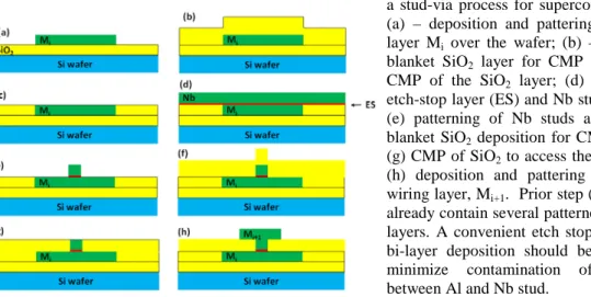
There are two possible realizations. The first is shown in figure 1 and referred to as a single etch and planarization (SEAP) process. Here, the bottom Nb wiring layer Mi is deposited and patterned,
figure 1(a). This layer is then planarized by depositing a thick layer of SiO2 [figure 1(b)] with
subsequent CMP to get the planar structure shown in figure 1(c). After this, Nb deposition for subsequent studs follows, figure 1(d). Since Nb studs need to be etched while stopping on the bottom Nb wiring, it is useful to have a good etch stop (ES) layer – a material with a lower etch rate than Nb. This ES layer must not degrade the superconducting properties of the interface in order to maintain high critical current in the superconducting state. There are very few materials suitable for this, and a thin layer of aluminium (a few nanometers thick) is one of them. After etching the studs, figure 1(e), the process flow repeats planarization steps (b) and (c) to planarize studs and open access to their top surface, figure 1(g). Finally, the top Nb wiring layer is deposited and patterned to complete the via-stud interconnects between a pair of Nb layers Mi and Mi+1. The process can further be repeated for the
next pair of wiring layers Mi+1 and Mi+2 and so on in a straightforward manner. It also allows for
stacking studs on top of each other.
Figure 1. Cross sections of the SEAP version of a stud-via process for superconducting circuits: (a) – deposition and pattering of (Nb) wiring layer Mi over the wafer; (b) – deposition of a
blanket SiO2 layer for CMP planarization; (c)
CMP of the SiO2 layer; (d) deposition of an
etch-stop layer (ES) and Nb stud metal bi-layer; (e) patterning of Nb studs and ES layer; (f) blanket SiO2 deposition for CMP planarization;
(g) CMP of SiO2 to access the top of Nb studs;
(h) deposition and pattering of the next Nb wiring layer, Mi+1. Prior step (a) the wafer may
already contain several patterned and planarized layers. A convenient etch stop layer is Al. The bi-layer deposition should be done in-situ to minimize contamination of the interface between Al and Nb stud.
The described process can be simplified by noticing that the structure formed after stud etching, figure 1(e), resembles the standard trilayer-type SNS Josephson junction where the base electrode is bottom wiring layer Mi, the counter (top) electrode is the stud, and the Al etch stop layer is N-layer or
Al-AlOx barrier layer in tunnel junction trilayers [6] without oxidation. Therefore, the stud-via
formation can be done in the same manner as the formation of Josephson tunnel junctions in a whole-wafer trilayer process [6] with the addition of planarization [8]. This second version of the stud-via process, shown in figure 2, is referred to as a dual-etch and planarization (DEAP) process.
11th European Conference on Applied Superconductivity (EUCAS2013) IOP Publishing
Journal of Physics: Conference Series 507 (2014) 042043 doi:10.1088/1742-6596/507/4/042043
Instead of depositing a single wiring layer as in the previous (SEAP) version, in this process each wiring layer is deposited in-situ as a Nb/Al/Nb trilayer, figure 2(a). The top layer of the trilayer is then patterned by photolithography and dry etching to form Nb studs as shown in figure 2(b). Aluminium serves as an excellent etch-stop layer for etching Nb in F-based chemistries. Then, the bottom electrode of the trilayer is patterned in Cl-based chemistry to etch through the Al layer and form the wiring pattern Mi. Etching is followed by blanket SiO2 deposition and CMP to access the tops of Nb
studs, figure 2(e). Then, the next layer Mi+1 is deposited as a Nb/Al/Nb trilayer and patterned in the
same manner to form the next layer of interconnects, and so on. If no more stud-vias are required above, a single metal wiring layer can be deposited. The described processing unit needs to be repeated as many times as there are wiring layers in the full process.
Figure 2. Cross-sections of Nb/Al/Nb trilayer-based (DEAP) stud-via process: (a) Nb/Al/Nb in-situ trilayer deposition; (b) patterning of the top electrode to etch Nb studs; (c) pattering of the bottom electrode to form wiring layer Mi; (d)
blanket SiO2 deposition for planarization by CMP;
(e) CMP down to the tops of Nb studs; (f) Nb/Al/Nb wiring layer deposition to form wiring layer Mi+1 and Nb stud to contact next layer Mi+2.
If no additional stud-vias are required above, a single Nb wiring layer Mi+1 can be deposited
instead. This process is to be repeated as many times as there are wiring layers in the entire process.
3. Stud-via fabrication
Nb/Al/Nb trilayers were deposited over 200-mm Si wafers with 500 nm of thermal oxide. The target thickness of the top Nb layer (Nb studs) was 250 nm, and of the bottom layer and the wiring layer was 200 nm. The thickness of the Al etch-stop layer was 8 nm. The photolithography was done using a positive deep-UV photoresist, bottom antireflection coating, Canon FPA-3000 EX4 248-nm stepper with 5x reduction and 250-nm nominal resolution. The circular shape for stud definition was implemented with diameters from 200 nm to 15 µm. The typical SEM images are shown in figure 3.
Figure 3. SEM images of the photoresist mask and etched Nb features: (a) tilted view of 400-nm photoresist posts masking Nb/Al/Nb trilayer used for stud-via definition; (b) top view of a photoresist post with design diameter of 250 nm, showing the automated CD measurement of the mean diameter using 48 points around the feature perimeter and giving 113.9 nm (right upper corner).
Nb etching was done using the high density plasma etching chamber of an Applied Materials Centura system with end-point detection. The results are shown in figure 4. Etching of the bottom wire was done in a Cl-based chemistry to break through the Al etch-stop layer first. A SiO2 film was deposited
using plasma-enhanced chemical vapor deposition (PECVD) from SiH4/N2O/Ar mixture for the
subsequent CMP using Applied Materials Mirra polisher.
11th European Conference on Applied Superconductivity (EUCAS2013) IOP Publishing
Journal of Physics: Conference Series 507 (2014) 042043 doi:10.1088/1742-6596/507/4/042043
Figure 4. Etched Nb studs with various diameters on top of bottom Nb wire: (a) 270-nm design diameter, 600-nm surround; (b) 280-600-nm design diameter, 100-600-nm surround. The bottom wire has an L-shape that with the corresponding L-shape in the top wire will form a cross-bridge Kelvin resistor (CBKR) configuration for electric measurements of studs. (c) The bottom diameter of the etched Nb studs as a function of the design diameter.
We have found that the size of the photoresist features and etched Nb studs can be well described by the relationship dw = k(d
2−d c
2
)1/2− b for d > dc, and d = 0 for d ≤ dc, as shown in figure 4(c). Here
d is the design diameter, dc is a photolighography cut-off size that depends on the photolithography
parameters, and b is the process bias. The scaling factor k characterizes the accuracy of the projection optics and SEM magnification. We have found that for the stable and optimized process dc≈ 250 nm,
k = 1±0.7%, and b is within the range of ± 50 nm.
The top wiring layer of Nb was deposited and patterned similarly to the bottom wiring and with the same overlap. The SEM picture of the completed stud-via structure is shown in figure 5.
0 100 200 300 400 500 0 1 2 3 4 5 6 7 8 I 1 /2 (mAc 1 /2)
Design diameter of Nb studs (nm)
c1r4 c4r4 c2r4 c3r4 c5r4 Ic = Jcπd 2 av/4, dc= 250 nm, b = - 85 nm dc= 285 nm, b = - 50 nm dav = (d 2 -d2 c) 1/2 - b Jc = 298 mA/µm2 (b)
Figure 5. (a) SEM image of the completed stud-via structure with 350-nm stud between two L-shaped wires. Clearly visible is the top Nb wire, lighter blurry image is the bottom wire as seen through the planarized SiO2
dielectric. The outline of the stud can be also seen due to a difference in niobium grain structure. (b) Critical current, Ic, of the fabricated Nb stud-vias along with the fits to Ic = Jcπdav2/4, where Jc = 0.3 A/µm2 is the critical
current density and dav is the mean of the top and bottom diameters of the fabricated studs, shown for two values
of the lithography cut-off parameter and process bias: d0 = 250 nm b = − 85 nm, and d0 =290 nm b = −50 nm.
4. Electrical test results and discussion
The critical currents, Ic, of the fabricated stud-vias are shown in figure 5(b). Ic scales with the actual
area of the studs. The current density Jcwas found to be 3∙10 7
A/cm2 (0.3 A/µm2), only about a factor of 2.5 lower than the Ginzburg-Landau depairing critical current density Jc
GL
= (2/3)3/2Bc/(µ0λ) in our
films, where µ0 = 4π∙10−7 H/m, Bc - the thermodynamic critical magnetic field, λ – the magnetic field
penetration depth [9]. Indeed, for Nb at 4.2 K, Bc≈ 0.145 T [10] and λ is in the range from 80 nm to
90 nm for our films. This gives Jc GL
in the range from 7x10⁷ A/cm2 to 8x10⁷ A/cm2. In the actual structure, the Jc should be somewhat lower than Jc
GL
of the film due to the presence of an 8-nm Al
11th European Conference on Applied Superconductivity (EUCAS2013) IOP Publishing
Journal of Physics: Conference Series 507 (2014) 042043 doi:10.1088/1742-6596/507/4/042043
etch-stop layer at the interface between the Nb stud and the bottom Nb wire. On the other hand, in the studied range, the diameter of the studs is larger than 4ξ, where ξ is the coherence length that in our films is about 20 nm. Hence, instead of the depairing, the stud critical current can be caused by the entry and motion of Abrikosov vortices when the current-induced magnetic field at the stud surface reaches Hc1. This gives an estimate for the critical current density jc = Hc1/(µ0λ), where
Hc1 = Hcln(κ+0.08)/(√2κ) [11]. Using κ = λ/ξ = 4 for our films, we get jc ≈ 0.36 A/µm 2
in a perfect agreement with the Jc observed in the fabricated Nb stud-vias.
Independently of the actual critical current mechanism, the observed critical currents are more than sufficient for the use of stud-vias in superconducting integrated circuits for interlayer connections. At
d = 0.5 µm the critical currents of stud-vias exceed those observed in etched contact holes of the same
diameter filled with deposited Nb metal.
5. Conclusions
We have developed and demonstrated a novel process for making deep sub-µm superconducting multilayer interconnects for use in VLSI and ULSI superconductive digital circuits. These interconnects are formed using Nb/Al/Nb trilayer wiring layers by etching Nb studs in the top layer and Nb wires in the bottom layer of the trilayers with subsequent planarization of the formed interconnects by dielectric CMP. The purpose of this process development is to replace the currently used etched-contact holes filled with sputtered Nb that are too big for VLSI SFQ circuits. Nb stud-vias with diameters as small as 150 nm have been fabricated by the developed process. For the design diameters ≥280 nm, the yield of the fabricated Nb stud-vias was 100% on the test structures available. The critical currents of the obtained Nb stud-vias approach the maximum possible superconducting currents for Nb and are certainly sufficient for interconnects in superconducting VLSI circuits.
Acknowledgement
The authors would like to thank Dr. Marc Manheimer and Dr. Scott Holmes for their interest and support of this work. This work was sponsored by the IARPA under Air Force Contract FA8721-05-C-0002. Opinions, interpretations, conclusions, and recommendations are those of the authors, and not necessarily endorsed by the United States Government.
References
[1] Likharev K and Semenov V 1991 IEEE Trans. Appl. Supercond. 1 3
[2] Nagasawa S, Satoh T, Hinode K, et al. 2009 Physica C 469 1578; Hidaka M, Nagasawa S, Hinode K, and Satoh T 2008 IEICE Trans. Electron. E91-C 318; Nagasawa S, Hinode K, Satoh T, Akaike H, Kitagawa Y, and Hidaka M 2004 Physica C 412-414 1429
[3] Tolpygo SK, Amparo D, Hunt RT, et al. 2011 IEEE Trans. Appl. Supercond. 21 119; Tolpygo SK, Yohannes D, Hunt RT, et al. 2007 IEEE Trans. Appl. Supercond. 17 946
[4] Kerber GL, Abelson LA, Edwards K, et al. 2003 IEEE Trans. Appl. Supercond. 13 82; Abelson LA and Kerber GL 2004 Proc. IEEE 92 1517
[5] Numata H and Tahara S 2001 IEICE Trans. Electron. E84-C 2
[6] Gurvitch M, Washington MA, and Huggins HA 1983 Appl. Phys. Lett. 42 472
[7] Steigervald JM, Murarka SP, and Gutmann RJ 1997 Chemical Mechanical Planarization of
Microelectronic Materials (John Wiley & Sons, Inc., New York) 129
[8] Ketchen M, Pearson D, Kleinsasser AW et al. 1991 Appl. Phys. Lett. 59 2609; Bao Z, Bhushan M, Han S, and Lukens JE 1995 IEEE Trans. Appl. Supercond. 5 2731
[9] Ginzburg VL and Landau LD 1950 Zh. Experim. i Teor. Fiz. 20 1064; Ginzburg VL 1958
Doklady Akademii Nauk SSSR, 118 467; Tinkham M 1996 Introduction to Superconductivity
(New York: McGraw-Hill) pp 124-125, 2nd ed; Bardeen J 1962 Rev. Mod. Phys. 34 667 [10] French RA 1968 Cryogenics 8 301
[11] Abrikosov AA 1957 Sov. Phys. JETP 5 1174
11th European Conference on Applied Superconductivity (EUCAS2013) IOP Publishing
Journal of Physics: Conference Series 507 (2014) 042043 doi:10.1088/1742-6596/507/4/042043