Defects, Thermal Phenomena and Design in
Photonic Crystal Systems
by
David Lik Chin Chan
M.Phys. (Hons.) University of Oxford, United Kingdom (2001)
Submitted to the Department of Physics
in partial fulfillment of the requirements for the degree of
Doctor of Philosophy
at the
MASSACHUSETTS INSTITUTE OF TECHNOLOGY
September 2006
@
Massachusetts Institute of Technology 2006. All rights reserved.
Author ...
...
Department of Physics
July 28, 2006
Certified by ... ....
.
Jo•
D.:Joannopoulos
Francis Wright Davis Professor of Physics
Thesis Supervisor
-I.-Accepted by...v-.-.-.-.
....
:
..
Thomas J. 9ytak
Associate Department Head for E cation
MASSACHUSETTS INSTITUTE OF TECHNOLOGY
JUL
0 2 2007
RCHLIBRARIES
Defects, Thermal Phenomena and Design in Photonic
Crystal Systems
by
David Lik Chin Chan
M.Phys. (Hons.) University of Oxford, United Kingdom (2001)
Submitted to the Department of Physics on July 28, 2006, in partial fulfillment of the
requirements for the degree of Doctor of Philosophy
Abstract
The physics of blackbodies has been an ongoing source of fascination and scientific research for over a hundred years. Kirchhoff's law states that emissivity and absorp-tivity are equal for an object in thermal equilibrium. Coupled with the Second Law of Thermodynamics, one can show that no object can emit more than a blackbody at any given frequency, direction or polarization. While this provides a theoretical maximum to the intensity of thermal emission from an object, few come even close to the level of emission exhibited by a blackbody. Thus, there is much room for research into enhancing thermal radiation from many different types of materials.
The ability to modify or tailor the thermal emission profile of an object is of great importance and interest in many areas of applied physics and engineering. It turns out that thermal emission spectra can be changed by altering the geometry of the system or the materials used. For instance, nanoscale patterning can enhance emission at certain frequencies, while point defects can localize light at microcavities. General periodic electromagnetic structures, also known as photonic crystals, are therefore a natural medium in which to carry out such investigations, since they are metallodielectric systems that lend themselves relatively easily to sub-wavelength scale patterning and design.
This research program aims to study, through both theoretical and computational means, physical phenomena that drive thermal emission in photonic crystals and the design of point defects in the presence of fabrication constraints.
First, we explore point defect geometries in inverted opal photonic crystals that can be fabricated by colloidal self-assembly. We identify and study substitutional point defects that introduce a usable defect band into the photonic band gap. It is found that a silica sphere of radius between 0.33a and 0.35a (where a is the lattice constant) introduces a triply degenerate state into the band gap. Reflectance and local density of states calculations are performed to verify the existence and frequency of this defect. Such a defect can be used as a microcavity for localizing light at a point,
with a quality factor
Q
that is limited primarily by the proximity of the defect to the surface of the photonic crystal and other such defects.Second, we present a useful framework within which we can understand some of the physical phenomena that drive thermal emission in one- and two-dimensionally periodic metallic photonic crystals, emphasizing phenomenology and physical intu-ition. We find that polarization and periodicity play key roles in determining the types of physical phenomena that can be excited in these systems. Promising struc-tures in both 1D and 2D systems are identified as good candidates for thermal design. We discuss how the emissive properties of these systems can be tailored to our needs. Third, we establish that the significant enhancement of thermal emission via
Q-matching, which has been possible in 1D systems only, can be extended to 2D systems by means of Fano resonances in the 2D system. We demonstrate through detailed nu-merical and analytical studies that the Fano resonances characteristic of 2D-periodic photonic crystal slabs can be understood in terms of a 1D-model, thereby showing the existence of essentially 1D behavior in a 2D system. Moreover, we show how properties of these spectra can be controlled by changing the geometrical parameters of the photonic crystals. This work provides a path to the creation of graybodies that have tailored thermal emission spectra, with highly anomalous behavior.
Fourth, we perform direct thermal emission calculations for 2D- and 3D-periodic photonic crystal slabs using stochastic electrodynamics following the Langevin ap-proach, implemented via an FDTD algorithm. We demonstrate that emissivity and absorptivity are equal, and thereby numerically verify Kirchhoff's law, by showing that such photonic crystal systems emit as much radiation as they absorb, for every frequency, up to statistical fluctuations. This has been an issue of great controversy because of experimental work indicating the violation of Kirchhoff's law. We also study the effect of surface termination on absorption and emission spectra from these systems.
Thesis Supervisor: John D. Joannopoulos Title: Francis Wright Davis Professor of Physics
Acknowledgments
I remember an exchange I had with my parents at the age of six, when I was just about to begin primary school in Hong Kong. As I embarked on this new phase of my life, I wanted to know what lay ahead, so that I could have something to look forward to. They told me there was secondary school. A little deflated, I asked them what happened after that. They said, university. That sounded more interesting. I asked again, and got a response along the lines of 'a Masters degree' - whatever that was. Determined to get to the end of this seemingly interminable road, I persisted. 'After a Masters degree, you can do a doctorate, and then people will call you Dr. Chan.' By this time, I was quite excited, because being called Dr. Chan sounded really cool.
'What is a doctorate?' I asked, with burning curiosity.
My parents looked at me, smiled, and said, 'It's the highest academic degree the world has to offer.'
It was like the first glimpse of Everest. My life changed that very moment. I knew I would not rest until I had achieved that goal. The subject did not matter, neither did my career choice. All that mattered was to pursue that dream; everything else I could worry about later. There are people who see the Ph.D. as a means to an end, whether that end be a career in research, teaching or industry; for me, the Ph.D. was the end.
Thus began the long road that would eventually lead to my doctoral studies, and this thesis, some twenty years later. What I did not anticipate, and is the raison d 'tre of these acknowledgments, is that a Ph.D. is not an individual endeavour. None of this work would have been possible without the kind, generous and selfless help and support I received from many people.
First and foremost, I would like to thank my research advisor, Prof. John Joanno-poulos, who has taught me far more than any individual I have encountered, save my parents. John is one of the most intelligent and charismatic people I know, and possesses the wonderful qualities of integrity, diligence and charm. He has been, and will continue to be, my professional and personal example. John does nothing
half-heartedly; every challenge and responsibility he takes upon himself he will execute with the utmost dedication, flair and attention to detail. As a result, he is the best scientist, teacher and mentor I have come across.
Yet his talents do not end here. He is a gifted manager of both time and people; the first to foster efficiency and productivity, and the second to promote harmony and collaboration within the research group. In the words of Dr. Oscar Alerhand, a former member of the group, 'John could run Goldman Sachs and Morgan Stanley in the morning, and still have time to do research in the afternoon!'
I am grateful to John for his help with practical matters also. He gave me inter-esting and challenging projects to work on, helped me get unstuck countless times, taught me the difference between apples and oranges, and gave me great leeway in pursuing other interests and commitments outside academics. (In the last five years, I took up sailing, swimming, skiing, figure skating, tennis, golf, singing, ballroom dancing, and to top it all off, I ran a marathon.) I am particularly grateful to John for his understanding of my career choice, his indispensable help in my job search, and his glowing recommendations that have enabled me to be fellowship-funded these five years.
I would like to acknowledge my research collaborators, without whose help none of this work would have been possible. It has been a great pleasure to work closely with Prof. Marin Solja6id, whose laid-back demeanour and good humour were particularly welcome during periods of frustration and lack of progress; thankfully, these periods were never long, because Marin, with his razor-sharp insight, would invariably put me on a new trajectory towards a solution. I also thank Prof. Steven Johnson, Dr. Elefterios Lidorikis and Ivan Celanovic for their help with many aspects of my research. I am grateful to Prof. Xiao-Gang Wen and Prof. Erich Ippen for serving on my thesis committee, and to the Kennedy Memorial Trust, MIT and the Croucher Foundation for providing me with fellowship funding.
It goes without saying that the graduate school experience is not one shaped by professors alone; my time at MIT has been enriched by the graduate students and post-docs I have interacted with. It has been a privilege to be part of John's research
group and to work with such brilliant colleagues; I can't think of any one in the group to whom I have not turned for help or just for a quick chat. In the midst of the somewhat monastic life of a graduate student, one source of simple and daily social sustenance was to have lunch with my CMT peers who are now my good buddies: Peter Bermel, Michael Levin, Cody Nave and Bas Overbosch. The daily ritual of deciding on a lunch venue, going there together, and talking about anything and everything under the sun created a strong sense of camaraderie and we really became a support network for each other. In particular, I'd like to give special thanks to Peter for being such a patient and helpful officemate. He was always willing to drop whatever he was doing to help me with the myriad computational and research problems I ran into, and it was delightfully reassuring that a computer guru was never more than three feet away!
My acknowledgments would not be complete without mentioning my good friends Tyler VanderWeele, Chris Lee and Olumuyiwa Temitope Ogunnika, who have been with me through thick and thin during my time in Cambridge. They were always glad to lend a listening ear and would go out of their way to cheer me up when I was down. My gratitude goes also to the many friends I have made through the MIT Graduate Christian Fellowship and Park Street Church in Boston.
I will close by dedicating this thesis to my loving parents, Ming Lee Chan and Stella Chan, who have given up so much for me. In addition to showering me with love, attention and encouragement, and teaching me never to be complacent and to always strive for excellence in everything I do, they gave me the two most important things in life: a world class education and a living faith in the Lord Jesus Christ. I praise God for saving my physical and spiritual life, for giving me strength and endurance to get through five years of graduate school, for surrounding me with wonderful friends during my time in Boston, and for giving me a reason to live and Someone to live for. Soli Deo Gloria!
Contents
1 Introduction 29
1.1 Overview of this work ... 31
1.2 A Whirlwind Tour of Photonic Crystals . ... 35
2 Point defect geometries in inverted opal photonic crystals 39 2.1 Introduction ... ... ... . 39
2.2 Point defect geometries ... 40
2.3 Characteristics of the defect state . ... . 43
2.4 Conclusion . . . .. . 52
3 Thermal emission and design in 1D-periodic metallic photonic crys-tal slabs 55 3.1 Introduction ... .. . ... .. 55
3.2 Physical phenomena that influence emission spectra . ... 57
3.3 Description of Numerical Methods . ... . 60
3.4 Role of Polarization ... ... 62
3.5 Periodicity and surface plasmons ... . . . . . . 68
3.6 Dependence on metallic material parameters . ... . . . . 70
3.7 Role of diffraction ... 73
3.8 Therm al design ... 75
3.9 Conclusion . . . .. . 77
crys-tal slabs 79
4.1 Introduction ... ... ... 79
4.2 Description of Numerical Methods ... . 80
4.3 Holes and dips ... ... 82
4.4 Hybrid structures ... 87
4.5 Thermal design ... ... ... 90
4.6 Conclusion ... ... 93
5 Emulating 1D resonant scattering behavior in a 2D system via Fano resonances 95 5.1 Introduction ... 95
5.2 Fano resonances in photonic crystals . ... 97
5.3 Analytical modeling ... ... . 99
5.4 Numerics ... ... 105
5.5 Thermal design ... ... .. ... 108
5.6 Conclusion ... 111
6 Direct calculation of thermal emission for 2D- and 3D-periodic
pho-tonic crystal slabs 113 6.1 Introduction ... 1136.2 Theory ... ... .. ... 115
6.2.1 Stochastic electrodynamics and the Langevin approach . . . . 115
6.2.2 Statistical properties of thermal fluctuations . ... 117
6.2.3 Calculation of emissivity ... . ... 118
6.2.4 Limitations of the method ... . 120
6.3 Description of numerical methods ... . 121
6.4 2D-periodic array of rods ... . ... 124
6.5 3D-periodic woodpile structure ... .. 127
6.6 3D-periodic metallodielectric structure . ... 132
6.7 Effect of surface termination ... .... 135
List of Figures
2-1 (Color) Two different styles of point defects (adapted from [10]). . . . 42
2-2 (Color) Bandstructure of photonic crystal with point defect mode. De-fect calculation performed with 3x3x3 supercell, with a (48,48,48) basis set, for shrunk silica sphere radius of 0.35a. The 3x3x3 supercell calcu-lation for the defect produced bandstructure with multiple folding of bands, and as such the band diagram for that calculation is not edify-ing to show. The most important result from that calculation, namely, the defect state frequency, was extracted, and this piece of information was incorporated into the above non-supercell bandstructure. ... 45
2-3 (Color) Reflectance spectrum of photonic crystal, with and without point defect. The dipole source is polarized in the [110] direction. The computational cell used had dimensions of 56x97x411 grid points, corresponding to 40 grid points per lattice constant. The photonic crystal slab was seated on a silicon substrate. A 2x2 supercell was used, and the simulation was run for 79,195 time steps. [Inset shows magnified version of reflectance dip due to defect.] . ... 47
2-4 Local density of states of photonic crystal, with point defect. We followed the Gilat-Raubenheimer method, using 8 evenly spaced k-points in the irreducible Brillouin zone. . ... 50
3-1 (Color) Here we show emittance (solid lines) and transmittance (dotted lines) spectra for y-polarized light emitted from a 1D-periodic metal slab with gaps, viewed at normal incidence. The Drude parameters used are co, = 1, wo = 0, 7 = 0.15(27rc/a) and
wp
= Vx/(27rc/a). In Panel (a), we fix the thickness of the slab at 1.0a (where a is the lattice constant of the slab) and vary the width of the gaps. In Panel (b), we hold the gap width constant at 0.2a and vary the thickness of the slab. 633-2 (Color) We show emittance (solid lines) and transmittance (dotted lines) spectra for a 1D-periodic metal slab for normal incidence and light polarized in the x-direction. The Drude parameters used are
(, = 1,
w
0 = 0,-
= 0.15(27rc/a) and wp =V/-T(27rc/a).
In Panel(a), we fix the thickness of the slab at 1.0a and vary the width of the gaps. In Panel (b), we hold the gap width constant at 0.2a and vary the thickness of the slab. In Panel (c), we study a corrugated metal slab of thickness 1.0a with a gutter of depth 0.5a, for different gutter widths. To better understand some of the modes exhibited in these panels, we show field profiles for peaks labeled I-V on the right half of the figure. Each pair of field plots shows E. on the left and Ez on the right. The edges of the computational cell are marked by thin black lines, while the metallic structure is shown in a translucent green color with dark green borders. The incident beam comes down from the top of the cell . ... .. .... ... 66
3-3 (Color) We present emittance (solid lines) and transmittance (dotted lines) spectra for a uniform metal slab with thin dielectric strips period-ically distributed on its surface. We consider light emitted/transmitted at normal incidence and polarized in the x-direction. The dielectric structure has a rectangular cross section of width 0.5a and height 0.2a, and sits on top of a metal slab of thickness 1.0a. The metal has Drude parameters c, = 1,
y
= 0.15(27rc/a) and w, =x/'V(27rc/a).
Panel (a) shows how emittance and transmittance vary for a few different dielec-tric constants of the strips. In Panel (b), we plot the frequencies of some of the peaks in Panel (a) as circles (red circles corresponding to red peaks, for example). In addition, we plot SP dispersion curves for uniform, semi-infinite metal-air and metal-dielectric structures (dotted lines). Top-left inset shows structure described by solid lines; bottom-right inset shows structure described by dotted lines. . ... 693-4 (Color) Emittance spectra for a corrugated metal slab, for normal in-cidence and y-polarization. The metal slab has thickness 1.0a, with gutters of depth 0.5a and width 0.5a. The metal has the usual Drude parameters of c, = 1, y = 0.15(27rc/a) and wp =
v/-0(27rc/a).
In Panel (a), we show how emittance changes with the plasmon frequency (wp). Panel (b) shows the variation of emittance with y, the parameter that controls material losses in the Drude model (in this case wp = v/). Note that in both panels, clear diffraction peaks are seen at w = 1, and the positions of these peaks do not change with either wp or y. . . . 713-5 (Color) We show emittance and transmittance spectra for a corru-gated metal slab produced by normally incident light, polarized in the y-direction, for two different gutter widths. The metal has Drude pa-rameters cE = 1,
y
= 0.15(27rc/a) andw,
= Vx/-(27rc/a). The metal slab has thickness 1.2a, with gutters of depth 0.2a and width 0.5a (red curve) and 0.8a (green curve). We observe that there are small emittance peaks at integer frequencies (w = 1, 2, 3, indicated by black arrows), caused by diffraction. Notice that no diffraction peaks are seen in the case of a uniform metal slab (black curve), because such a slab has continuous translational symmetry in the x-direction. Note also the sudden rise in transmittance and emittance above the plasmon frequency (wp 3.16), above which the metal is transparent. . ... 743-6 (Color) Panel (a) shows how emissive power for a corrugated metal slab changes with temperature of operation. The emission spectra is observed at normal incidence, polarized in the y-direction. The metal has Drude parameters e, = 1,
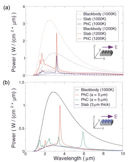
y/(27rc)
= 500cm- 1 and wp/(27rc) = 10540cm- 1. The metal slab has thickness 3pm, with gutters of depth 1.5/im and width 1.2pim. We show the spectra for the blackbody, the PhC, and the uniform metal slab (thickness 3pm) for two tempera-tures, 1000K and 1200K. Panel (b) shows how emissive power for a metal slab with dielectric strips changes with the lattice constant. The metal slab is of thickness 3pm, while the dielectric strips are of width 1.5pm, height 0.6t1m, and f = 2. Clearly, increasing the lattice con-stant increases the wavelength at which peak emission occurs. Note that the peaks arise from the excitation of surface plasmon modes. 764-1 (Color) Here we show emittance (solid lines) and transmittance (dotted lines) spectra for a 2D-periodic metal slab with circular holes, viewed at normal incidence and for y-polarized light. The Drude parameters used for the metal are Ec, = 1,
wo
= 0, y = 0.3(27rc/a) and w, = VT-(27rc/a). In Panel (a), we fix the thickness of the slab at 1.0a (where a is the lattice constant of the slab) and vary the radius of the holes. The black arrows indicate the peaks produced by the waveguide cut-off in the x-direction. In Panel (b), we keep the hole radius constant at 0.4a and vary the thickness of the slab. Here, we use arrows to indicate the peaks produced by diffraction. . ... . 834-2 (Color) We show emittance (solid lines) and transmittance (dotted lines) spectra for a 2D-periodic metal slab of thickness 1.0a with cir-cular dips, observed at normal incidence and y-polarization. The dips have a depth of 0.5a. The Drude parameters used are c, = 1, wo = 0, 7 = 0.3(27rc/a) and wp = v/'(21rc/a). We show spectra for two differ-ent radii of dips, keeping the slab thickness constant. . ... 86
4-3 (Color) Panel (a) shows emittance (solid lines) and transmittance (dot-ted lines) spectra for a 2D-periodic metal slab of thickness 1.0a with circular dielectric pucks for normal incidence and light polarized in the y-direction. The pucks have a radius of 0.4a and a thickness of 0.2a. The Drude parameters used for the metal are e, = 1, wo = 0,
7 = 0.3(27rc/a) and wp = V'-(27c/a). We show spectra for three
different dielectric constants for the circular puck. In Panel (b), we took the peaks labeled by arrows in Panel (a), and plotted them on a dispersion curve. (Note that the third red peak in Panel (a) coincides with a diffraction peak at frequency vi e 1.41.) We see that the dispersion of the peaks (lines with circles) lies between the metal-air dispersion and the metal-dielectric dispersion, for the corresponding dielectric constant. Therefore, it is quite plausible that these peaks are produced by surface plasmon modes. In Panel (c), we show the ther-mal emission spectrum for the same metal slab with pucks of dielectric constant e = 5 at temperature 1000K (we call it "PhC (model)"). We also show the blackbody spectrum at that temperature for comparison. The lattice constant was chosen to be a = 2.94pm. Panel (d) shows the thermal emission spectrum for the same system except that the "model" metal has been replaced by tungsten. We modeled tungsten with Drude parameters[55] E, = 1, wo = 0,
y/(2rc)
= 487cm- 1 and wp/(27rc) = 51700cm- 1, and we chose a = 2.941pm. We show the emis-sion spectra for a uniform tungsten slab of thickness a (without pucks) and a blackbody for comparison. . ... . 884-4 (Color) Here we show the thermal emission spectrum for a hybrid 2D-periodic structure consisting of a tungsten slab and a dielectric slab with holes. The metal slab is 1.0a thick while the dielectric slab (E = 5) is 0.2a thick with holes of radius 0.4a. We show emission of light polarized in the y-direction. In Panel (a), we display emission at two different temperatures. We chose a lattice constant of a = 2.00pm. In Panel (b), we show how the emissive power changes with lattice constant. In both panels, we show emission spectra for a uniform tungsten slab of thickness a without dielectric, and a blackbody, for com parison. . . . .. .. 91
5-1 (Color) Panel (a) shows some generic features associated with thermal radiation of common black/graybodies into air (the case of a perfect blackbody is denoted by solid lines, while an example of a graybody, a
uniform Si slab of thickness 0.75pm, is denoted by dashed lines); plot-ted is the thermal radiation intensity/dk.dk.dA for an exemplary case: k= = 0.838pm- 1 and ky = 0. First, black/graybodies have perfectly in-coherent and ultra-broad bandwidth thermal emission spectra. Next, as the temperature of such a body increases, the emission spectrum shifts to shorter wavelengths. Finally, bodies with lower absorption have weaker thermal emission; for example, a thin silicon slab is nearly transparent for infra-red light even at fairly high temperatures, so its thermal emission is very weak. Panel (b) shows FDTD calculations of the thermal emission spectra of the same Si slab as in Panel (a), but this time patterned as a square-lattice 2D-periodic photonic crystal slab of holes with radius r = 0.3pm, and lattice constant a = 1.5pum
(structure schematic shown in inset). Thermal radiation of such a body can display drastically different behavior than the one shown in Panel (a). First, a photonic crystal can produce very coherent thermal radia-tion, as implied by the narrowness of the emission peaks. Next, as one increases the temperature, the peak emission can shift to longer (in-stead of shorter) wavelengths. Finally, despite the near-transparency of Si, emissivity can be comparable to that of a perfect blackbody for certain frequencies ... .... ... 98
5-2 (Color) FDTD simulations of a photonic crystal slab (PhC) of thickness 0.5a with Re(E) = 12 for incident electric field polarized in the y-direction. (a) Transmission and absorption spectra for PhC slab, for
k, = 0.2(2r/a), with Im(c) . 0.005 (chosen to maximize absorption for the first peak), displaying 4 Fano resonance peaks. (b) Band diagram of the photonic crystal slab modes in the case of an infinitesimally small amount of absorption. Note that Fano resonances in Panel (a) occur exactly at those frequencies for which there is a guided mode of the PhC that has k. = 0.2(27r/a). ... 100
5-3 (Color) Comparison between theory and simulation, for the first two Fano peaks shown in Fig. 5-2a. The parameters of the theory (wo and
-) were calibrated by fitting the red line (theory without absorption) to
the red circles (simulation without absorption). The black line gives the prediction of theory for the absorptive case; the black circles represent the results from simulation with absorption. (The fraction of energy in dielectric (() was 90% for the first peak and 95% for the second, done in a separate FDTD calculation.) ... ... 107
5-4 (Color) Variation of Fano absorption peak frequency as function of angle of incidence (in degrees); rotation angle is around y-axis, and electric field is polarized along y-direction. (a) First peak. (b) Second peak. The change in frequency for the second peak is much smaller than that for the first. The angles are different for the top and bottom panels even though the ks's used are the same because 0 is a function of both k, and w.u ... ... 110
6-1 (Color) Bandstructure for a 2D-periodic array of perfect metal rods of radius 0.2a. We show bands along F-X and F-M. The resolution is 40 grid points per a. We consider only TM modes, for which the electric field is polarized along the axes of the rods. We notice large band gaps in the system where light is forbidden from propagating, specifically from 0 to 0.52c/a and from 0.72c/a to 0.86c/a. . ... 125
6-2 (Color) Comparison between absorption and thermal emission (aver-aged over 40 runs) from a 2D-periodic PhC slab of metal rods and a uniform slab, for TM modes at normal incidence. For the slab of rods, we use a long computational cell of 1x8 rods. For the metal, we use the Drude model with parameters c, = 1, 7 = 0.3(2irc/a), 47ra = 10(4 2c2/a2). We see good agreement between the emissivity (green and blue solid lines) and the absorptivity (black and red dashed lines). We notice also that the emissivity of a 2D slab of rods exceeds that of a uniform slab at all frequencies. The greatest enhancement comes from the non-gapped regions, where the enhancement can be as high as a factor of 4. Translucent yellow shading indicates regions of pseudogap for such a slab of imperfect metal rods, inferred from the absorption/emission spectrum. . ... .. 126
6-3 (Color) Bandstructure for a 3D-periodic woodpile structure made of perfect metal rods with square cross section of width 0.25a. We show bands along F-X and F-Z. The resolution is 30 grid points per a. We consider modes with all polarizations. We notice a large band gap in the system where light is forbidden from propagating, specifically from 0 to 0.42c/a. ... .. .. ... 129
6-4 (Color) Comparison between absorption and thermal emission (aver-aged over 40 runs) from a slab of 3D-periodic woodpile made of metal rods, at normal incidence. We use a long computational cell with two unit cells of the woodpile structure in the z-direction. For the metal, we use the Drude model with parameters E, = 1, y = 0.3(2irc/a),
4roa
= 10(47r2C2/a2). The frequency resolution is 0.001c/a. We see good agreement between the emissivity (green and blue solid lines) and the absorptivity (black and red dashed lines). We notice also that the emission of the woodpile structure exceeds that of a uniform slab at all frequencies. The greatest enhancement comes from the non-gapped region above 0.4c/a, where the enhancement can be as high as a factor of 4. Translucent yellow shading indicates regions of pseudogap for such a woodpile slab structure made of imperfect metal rods, inferred from the absorption/emission spectrum. . ... 1306-5 (Color) Bandstructure for a 3D-periodic metallodielectric structure made of perfect metal spheres of radius 0.177a in a background of Teflon (c = 2.1). We show bands along F-X and F-L. The resolution is 32 grid points per a. We consider modes with all polarizations. We notice a complete band gap in the system where light is forbidden from propagating, specifically from 0.54c/a to 0.63c/a. . ... 133
6-6 (Color) Comparison between absorption and thermal emission (aver-aged over 40 runs) from a slab of 3D-periodic metallodielectric struc-ture made of metal spheres in a Teflon background, at normal in-cidence. We use a long computational cell with two unit cells of the metallodielectric structure in the z-direction. For the metal, we used the Drude model with parameters ec, = 1, y = 0.3(27rc/a), 4ira = 10(47r2c2/a2). Here, we use a lower frequency resolution of 0.Olc/a in order to decrease the duration of each run. We see good agreement between the emissivity (green and blue solid lines) and the absorptivity (black and red dashed lines). We notice also that the emis-sion of the metallodielectric structure exceeds that of a uniform slab at all frequencies above 0.1c/a. The greatest enhancement comes from the non-gapped region around 0.8c/a, where the enhancement can be as high as a factor of 6. Note that the emissivity in that region is close to unity. Note also that the decreased run time leads to lower frequency resolution, as evidenced by the smoother spectrum. However, the size of the fluctuations remains unchanged (compare with Fig. 6-4), since is determined by the number of runs used in ensemble-averaging. . . 134
6-7 (Color) Absorbance/emittance spectrum for a woodpile PhC slab made
of imperfect metal rods for 5 different surface terminations. Light po-larized along x is incident from the top of the cell. We use a long computational cell with two unit cells of the woodpile structure in the z-direction. For the metal, we used the Drude model with parameters c0 = 1, , = 0.3(27rc/a), 47ro = 10(4r2C2/a2). The inset is a schematic (lengths not to scale) indicating the surface terminations chosen. For all calculations, we keep the thickness of the slab to about two unit cells, so changing the surface termination amounts to shifting the struc-ture within a two-unit-cell-thick slab 'mask' which remains stationary as the structure is shifted, such that the total amount of material is kept constant. For instance, for 'STO', the structure used is that be-tween the two black lines, while for 'ST6', it is what lies bebe-tween the two blue lines. 'ST7' appears to have the highest absorption/emission at all frequencies. ... 136
List of Tables
3.1 The waveguide cut-off frequencies associated with different gap widths in Fig. 3-la, and their corresponding half-wavelengths. . ... 62 3.2 The waveguide resonant frequencies associated with the red curve in
Fig. 3-1b, and their corresponding half-wavelengths, calculated and predicted. ... ... 64
Chapter 1
Introduction
Ever since the discovery of an electromagnetic band gap in certain periodic dielectric structures[82] some twenty years ago, research into photonic band gap materials has taken off, creating a whole new subfield of physics. Lying at the intersection of solid state physics, materials science and electrical engineering, these fascinating materials are characterized by their possession of a photonic band gap, a range of frequencies in which light is forbidden from propagating. As such, these materials, also known as photonic crystals, can be thought of as the electromagnetic analogue of semicon-ductors, which possess electronic band gap regions where electrons are forbidden to propagate. If the semiconductor revolution, which forever changed the landscape of electronics research, is anything to go by, many believe that photonic crystals will usher in a similar revolution in the fields of optics, telecommunications and optical computing. Some believe it already has.
Prior to the advent of photonic crystals, a researcher in the field of optics had at her disposal a few important ideas from geometrical and wave optics, which were sufficient for most problems related to refraction, reflection, diffraction and interference[29]. In telecommunications, optical fibers were all the rage; they could trap light in a cylindrical tube and even bend it around a corner (though not too sharp a corner). Consequently, a fiber optic infrastructure has been built in many places around the world, carrying far more information with much lower losses than conventional electric coaxial cables.
Versatile as these fibers are, their operation is based on a very simple physical idea: total internal reflection. As such, they are limited in two ways. Total internal reflection occurs when the angle of incidence exceeds a critical angle; below this threshold, refraction occurs. A fiber, therefore, cannot be bent into too small a radius of curvature before the light in the inner core starts leaking out. The second problem arises from the design of optical fibers. Total internal reflection occurs when light from a high dielectric medium meets a low dielectric medium. It cannot occur the other way around. Thus, the light necessarily travels in a region of high dielectric, surrounded by a low dielectric cladding. It so happens that most materials have at least some absorptive losses, so that the high index core ends up absorbing a sizable fraction of the power over long distances, leaving a weakened signal at the other end. Furthermore, nonlinearities, which are present in most materials, put a limit on the maximum power that can be transmitted.
Both these problems can be avoided by using photonic crystals. A multilayer film can be wrapped into an omnidirectional waveguide with superior confinement (no critical angle). A one-dimensional line defect in a material with a complete photonic band gap can serve as a waveguide, also with no critical angle; if two such line defects meet to form a corner, a resonant cavity can be placed at that corner and tuned so as to promote 100% transmission and 0% reflection around the bend. All these configurations can be designed so that the light travels in a region of air surrounded by bulk material. Thus, photonic crystals can overcome the limitations associated with optical fibers by offering omnidirectional confinement and light transmission in an air core. Moreover, as an illustration of the power and versatility of photonic crystals, one can design a channel drop filter consisting of a resonant cavity connecting two parallel waveguides, such that an input signal in one waveguide can be passed to the output channel of the other waveguide with minimal losses.
We have extolled the virtues of photonic crystals in the realm of optical design, but their merits do not end here. Far more than being a better technology, photonic crystals embody a new paradigm, a fundamentally new way of thinking about electro-magnetism in solid state systems. Because Maxwell's equations can be recast into the
form of a Hermitian eigenvalue problem involving vector differential operators (see section 1.2), we can plot dispersion curves, or bandstructure, for these systems, which give us great insight into the eigenmodes allowed by the system. What was previously understood as total internal reflection above a critical angle of incidence can, in the new paradigm, be understood as a region in w - k space that permits guided modes
to propagate. This new way of thinking has much in common with semiconductor physics; in fact, an extensive analogy may be drawn between the three-dimensional scalar eigenvalue problem in semiconductor physics and the three-dimensional vector eigenvalue problem in solid state electromagnetism.
Computational calculations for such systems are of great importance because they can serve as a pre-laboratory where novel geometries and structures can be tested and refined. One can have faith in relatively accurate correspondence between calcula-tion and experiment because Maxwell's equacalcula-tions are essentially exact in the linear regime of low photon-photon coupling, the regime in which photonic crystals are used. Reverting to the analogy with semiconductor physics, we expect computational cal-culations for photonic crystals to be more accurate than those for semiconductors, because electron-electron coupling is stronger in semiconductors than photon-photon coupling is in photonic crystals. As a result, bandstructure calculations and time-domain simulations have become indispensable tools in driving the field forward. In fact, these tools have become so standardized that they are freely and widely available to researchers in the field (e.g. MIT Photonic Bands).
1.1
Overview of this work
The goal of the present research is to shed light on a few important questions in the field of photonic crystal research today, namely,
1. How do fabrication constraints affect the design of defects in photonic crystals? 2. How can photonic crystals be used to modify and enhance thermal radiation? 3. Does Kirchhoff's law hold for a general photonic crystal, given recent
contro-versial experiments that suggest the contrary?
With regard to the first question, recently, there has been much interest in fab-ricating photonic crystals by means of colloidal self-assembly. Such a method is attractive because it offers a simpler and cheaper way of making three-dimensionally periodic photonic crystals, compared with conventional semiconductor nanofabrica-tion techniques, which, while being more precise, are significantly more expensive. However, the lower cost of manufacture comes with trade-offs. There is the problem of disorder and structural defects in the photonic crystal, which plague many such methods of self-assembly. This is especially important since disorder can destroy the photonic band gap in such materials. But even if we were to set aside this problem as an essentially experimental one, we would run into another, more theoretical, con-straint: that put on the design of the photonic crystal by the method of fabrication itself. For instance, Vlasov et al.[76] use a method of colloidal self-assembly that requires etching out self-assembled silica spheres in order to produce air gaps inside a background of silicon. However, the method of wet-etching necessitates a connected structure of silica spheres through which the wet-etching agent can permeate. Given the utility of point defects as microcavities for localizing light (we will discuss this further later in this chapter), there is, therefore, a need to identify a class of point defects that can be made using this method. This was the motivation for the work described in chapter 2.
The second question concerning the modification and enhancement of thermal ra-diation has been around for well over a century now. Ever since Planck[59], the physics of blackbodies has been a source of fascination and scientific research; properties of their thermal emission provided one of the most important clues for the discovery of quantum mechanics. Kirchhoff's law states that emissivity and absorptivity are equal in thermal equilibrium. Coupled with the Second Law of Thermodynamics, it is possible to show that no object can emit more than a blackbody at any given frequency, direction or polarization. While this provides a theoretical maximum to the intensity of thermal emission from an object, few come even close to the level of emission exhibited by a blackbody. In fact, uniform slabs of material are found to
be relatively poor emitters. Thus, there is much room for research into enhancing thermal radiation from many different types of materials.
The ability to modify or tailor the thermal emission profile of an object is of great importance and interest in many areas of applied physics and engineering. It turns out that thermal emission spectra can be changed by altering the geometry of the system or the materials used. Photonic crystals are therefore a natural medium in which to carry out such investigations, since they are metallodielectric systems that lend themselves relatively easily to sub-wavelength scale patterning and design. In light of this, a clear and physically intuitive understanding of the mechanisms that drive thermal emission in such systems is of great value in guiding thermal design.
Because of important inherent differences between one-dimensional (1D), two-dimensional (2D) and three-two-dimensional (3D) periodicity in photonic crystals, it is best to analyze crystals of different dimensionality separately. We focus on some of the most important physical phenomena that drive thermal emission. We do this with the intention of developing physical intuition and understanding of features of emission spectra. Once we have this intuitive understanding, we show how one can tailor the thermal emission properties of these structures to achieve one's design needs. We do this for both 1D- and 2D-periodic metallic photonic crystal slabs, covering a multitude of physical phenomena, including waveguide cut-offs, waveguide resonances, surface plasmons, slab resonances and diffraction peaks.
From the literature, it is clear that the idea of matching the radiative Q-factor of a system with its absorptive Q-factor in order to enhance emission is fundamentally a one-dimensional one. It is reducible to the problem of having one input channel, a resonant cavity, and one output channel. In such a setup, light emitted by the resonant cavity and the incident light interfere in such a way as to extremize the net outgoing wave. This complete cancellation of waves from the cavity and the incident/outgoing beam is unique to the one-dimensional world. However, it turns out that enhancement of thermal emission via Q-matching, which is usually observed in 1D systems only, can be extended to 2D systems by coupling into Fano resonances[19] in the 2D system. In other words, we demonstrate the existence of essentially 1D behavior in a 2D
system - a case of reduced dimensionality. We show through detailed numerical and analytical studies that the Fano resonances characteristic of 2D-periodic photonic crystal slabs can be understood in terms of a 1D-model based on Q-matching.
The third and final question we asked concerns the validity of Kirchhoff's law when applied to a general photonic crystal structure. This was originally proven analytically for a 1D uniform slab. One may well wonder whether such a law, which makes sense intuitively given the principle of detailed balance, holds for the more general case of a photonic crystal. But the question took on a new relevance in 2003, when intriguing experiments by Lin et al.[45, 42] seemed to indicate that the thermal radiation from metallic photonic crystals might even exceed that of a blackbody in free space. The possibility of thermal nonequilibrium during the measurement process has been acknowledged[46]. The controversy was partly addressed by Luo et al. [48], who performed a direct emission calculation for a 2D-periodic array of circular rods, and showed that thermal emissivity was equal to absorptivity, apart from statistical fluctuations. However, Lin's work was done on 3D-periodic photonic crystal structures. In the final part of this thesis, we extend the work of Luo et al. by applying the same methodology of stochastic electrodynamics to two fully 3D-periodic photonic crystal structures: a woodpile[74] (similar to that studied by Lin et al.) and a diamond metallodielectric structure[20]. We also consider the role of surface termination in determining the emission spectrum of a woodpile structure. As a bonus, we find that certain 3D-periodic structures have much higher thermal emission compared with a uniform slab; these high-emission structures should be very useful in thermophotovoltaic and incandescent lighting applications, where luminous efficiency is paramount.
The outline of the thesis is as follows: the rest of this chapter describes the basic physics of photonic crystals and introduces important ideas that will come up later in this work. Chapter 2 investigates point defect geometries in inverted opal photonic crystals fabricated by colloidal self-assembly. In Chapters 3 and 4, we study thermal emission and design in 1D- and 2D-periodic metallic photonic crystal slabs, respectively. Chapter 5 applies a 1D-model of thermal emission enhancement based
on Q-matching to Fano resonances in a 2D-periodic system, with intriguing results. In Chapter 6, we present a direct calculation of thermal emission in 3D-periodic photonic crystals, using the methodology of stochastic electrodynamics previously developed by Luo et al.[48], and demonstrate the validity of Kirchhoff's law in 3D-periodic photonic crystals. Finally, in Chapter 7, we summarize the important ideas of this thesis, and conclude our exposition.
1.2
A Whirlwind Tour of Photonic Crystals
The laws of classical electromagnetism were first presented to the Royal Society in London by James Clerk Maxwell in 1864. These four equations governed the behavior of electric and magnetic fields and their interactions with materials. As long as mate-rials could be modeled by their dielectric permittivity (E) and magnetic permeability (p), one could, in theory, work out the electric and magnetic fields generated by the system for a given set of boundary conditions. These coupled three-dimensional vector differential equations were not trivial to solve in general. Nonetheless, the description of electromagnetism in the form of a classical field theory was complete.
In the early twentieth century, quantum mechanics was being developed, and one of the most important mathematical frameworks being used in that field was that of the eigenvalue problem. The time-independent Schrodinger equation, which governs the behavior of a particle of mass m moving in a potential well V(r), can be written
H'iJ(r) = EiT(r)
where H = - -V2 + V(r) is the Hamiltonian (a scalar differential operator), Ti(r) is the wavefunction (a complex scalar field), and Ei is the energy eigenvalue (a real scalar). The wavefunction Ti(r), when operated on by the Hamiltonian H, is simply the wavefunction itself multiplied by a constant Ei. There are generally many solu-tions (labeled by i) to this eigenvalue equation, each of which has an eigenfunction Ti(r) and an eigenvalue Ei. Because H is Hermitian (f ¢*HodV = f(HO)*?PdV),
the eigenvalues Ei are all real, and the eigenfunctions Ti(r) are mutually orthogonal. It turns out that Maxwell's equations can be combined in such a way as to take the form of a Hermitian eigenvalue equation. The magnetic field H at position r is given by
eHi(r)
=( Hi(r)where
E
= V x ×-Vx is a real vector differential operator, wi is the frequency eigenvalue, and c is the speed of light. The similarity is obvious between the elec-tromagnetic eigenvalue problem and the quantum mechanical eigenvalue problem. It turns out theE,
as defined above, is a Hermitian operator, so we can expect the eigenvalues wi to be real and the eigenfunctions Hi(r) to be orthogonal. Because of the similarities between quantum mechanics and electromagnetism, many of the ideas and theorems from the former field, such as Bloch's theorem for periodic potentials and bandstructure calculations, may be applied to the latter.In their most general form, photonic crystals are periodic structures made of metal or dielectric. This periodicity may be in one, two or three dimensions. It is fair to say that photonic crystals create the electromagnetic equivalent of the periodic electronic potentials one sees so often in solid state physics. Out of these periodic po-tentials arise electronic (photonic) band gaps, which are ranges of energy (frequency) in which electrons (photons) are forbidden from propagating. One interesting feature of electromagnetism in dielectric media is that there is no fundamental length scale, unlike Schrodinger's equation, for which the natural length scale is the Bohr radius. Therefore, it is possible to take an existing solution for a particular photonic crystal system, and scale it up or down in physical size and frequency. It is also possible to take advantage of mirror plane symmetry in photonic crystal systems and separate the eigenmodes into transverse magnetic (TM) and transverse electric (TE) modes.
What makes photonic crystals truly versatile as building blocks for optical systems is the possibility of introducing deliberately designed defects. A point defect can localize light at a point; a line defect can be used as a waveguide. The basic principle is the same: light of a particular frequency is forbidden from propagating in the
surrounding bulk material because of the photonic band gap that exists in the bulk; as a result, the light is confined to the region of the defect, where a defect mode exists. Furthermore, just as one can suppress absorption of light by using a band gap, so one can suppress emission of light by the same method. The ideas and tools that are available for designing absorption are equally applicable to thermal emission, because of Kirchhoff's law. There is, therefore, much room for creativity and research in using photonic crystals to tailor thermal emission to one's needs, and indeed, it is with this topic that the greater part of this thesis will be concerned.
Chapter 2
Point defect geometries in inverted
opal photonic crystals
In this chapter, we study point defect geometries in inverted opal photonic crystals that can be easily fabricated by means of colloidal self-assembly. Two broad classes of defects are considered: substitutional and interstitial. Substitutional point defects are found to introduce a usable defect band into the photonic band gap. This can be done by using a silica sphere of radius between 0.33a and 0.35a (where a is the lattice constant). The state is triply degenerate. Reflectance and local density of states calculations are performed to verify the existence and frequency of this defect. The point defect can be made by pre-coating shrunk silica spheres with a thin layer of silicon. Such a defect can be used as a microcavity for localizing light at a point, with a quality factor
Q
that is limited primarily by the proximity of the defect to the surface of the photonic crystal and other such defects.2.1
Introduction
Recently, there has been much interest in fabricating photonic crystals by means of colloidal self-assembly[32, 76, 30, 77, 57, 65, 8, 47]. Such a method is attractive because it offers a simpler and cheaper way of making three-dimensionally periodic photonic crystals, compared with conventional semiconductor nanofabrication
tech-niques. Work has been done to show that self-organizing systems that self-assemble into large-scale photonic crystals can have photonic band gaps (PBGs) or pseudo-gaps in the near-visible frequency regime[9, 6, 67, 4, 78, 85, 49, 60, 33, 37, 34, 71, 40]. Natural assembly of colloidal microspheres yields irregular, polycrystalline photonic crystals with many structural defects that can destroy the PBG. However, it turns out that strong capillary forces at a meniscus between a substrate and a colloidal sol can induce crystallization of spheres into a 3D array of controllable thickness. Sweeping this meniscus slowly across a vertically placed substrate by solvent evaporation leads to the deposition of thin planar opals. This technique has been used by Vlasov et al.[76] to produce inverted opal photonic crystals with bandgaps at around 1.3 Mm.
Deliberately designed defects are desirable features in photonic crystals[62, 27]. A point defect, for example, with a mode localized within a complete PBG would give rise to a microcavity, while a line defect can be used as a waveguide[32, 35]. Microcavities and waveguides can be used as building blocks for optical devices and all-optical integrated circuits. There is, therefore, a need to design defects that can exist in the gap and be easily introduced into the bulk structure. Since colloidal self-assembly appears to be a promising and economical way of fabricating photonic crystals, we would like to identify a class of point defects that can be made using this method. This was the motivation for the work described in this chapter. Computa-tional calculations for such systems are of great importance because they can serve as a pre-laboratory where novel ideas of possible defect geometries are tested and refined. One can have faith in relatively accurate correspondence between calculation and experiment, since Maxwell's equations are essentially exact in the linear regime of low photon-photon coupling, the regime in which such crystals are used.
2.2
Point defect geometries
We consider an inverted opal structure, which is a face-centered cubic lattice of air spheres in a silicon background. Such a structure can be thought of as the inverse of the more familiar f.c.c. crystal of silicon spheres in air. Experimentally, synthetic
opals can be made by colloidal crystallization of an f.c.c. lattice of silica spheres, backfilling interstitial spaces with silicon, and then wet-etching out the silica spheres, leaving air spheres behind. However, the infiltration of the background with silicon is usually imperfect, leaving some air gaps in between the silica spheres. We take this imperfection into account in our simulations by building up the structure using air spheres with a 0.06a (where a is the lattice constant of the f.c.c. lattice; in all that follows, length scales will be given in units of a) coating of silicon, which leaves air gaps in the diagonal spaces between spheres. In the structure under study, the air spheres have a radius of 0.354a, so the silicon coating is about 17% of the radius of the air spheres. The air spheres are overlapping because the critical radius for the overlap of spheres in f.c.c. crystals is a/(2xf2) = 0.354a. We terminate the surface using a plane that cuts the spheres in half, because this appears to be more similar to what is produced in experiments by Vlasov et al.
In general, one can create a defect by adding or removing dielectric. The former method produces a dielectric defect while the latter gives an air defect[31]. Both are effective ways of introducing defects to a photonic crystal system, though there are connectivity issues that make the two methods different, depending on whether the crystal itself is dielectric- or air-connected (or both). It should also be noted that the orientation of the crystal can affect the reflectance measurements. It turns out that, for inverted opals, samples of higher quality can be obtained with surfaces normal to the [111] direction than the [100] direction. For this reason, most of our work involves studying crystals with [111] surface orientation. Furthermore, in experimental mea-surements, the wafer was placed on top of a silicon substrate. It was thought that the presence of the substrate could have a non-trivial effect on reflectance measurements. However, having performed calculations with and without the substrate, we find no significant differences.
Fig. 2-1 shows the two different defect geometries that we considered. An in-terstitial defect is designed to fit into the spaces between the larger spheres. A substitutional defect replaces an existing sphere.
substitutional
interstitial
defect
iterstitial
efect
Figure 2-1: (Color) Two different styles of point defects (adapted from [10]).
a
detect
small; otherwise, their presence in the colloidal self-assembly process would disrupt the structure of the rest of the crystal. The upper bound on the radius of the small sphere is $(I - $)a
=
0.146~. Single interstitial air and dielectric defects can be im- plemented by having small silica or silicon spheres, and were tried in our calculations. We also considered clumps of 7 or 8 such air and dielectric defects. The presence of interstitial air defects changes the connectivity of the system, since new air chan- nels have been created joining non-adjacent large air spheres. Interstitial dielectric spheres, however, only affect the system insofar as they fill in the 'holes' that were not completely backfilled with silicon. In any case, our results for these interstitial defect geometries revealed no particularly useful change in the bandstructure of these systems that could lead to the existence of a defect band in the gap. The change tended to either pull down some states from the upper bands into the gap, but only for certain wave vectors, or it destroyed the photonic band gap altogether. In the remainder of this chapter, we will restrict our attention t o substitutional defects.In the substitutional case, the outer radius must lie between 0 . 1 4 6 ~ and 0.354~: if less than the former, then the sphere will slide into an interstitial space; if greater than the latter, it will disrupt the packing of the structure.
A
relatively easy modification would be to reduce the size of the silica spheres used to create the structure. Note, however, that if the radius of the silica spheres is decreased below 0.354a, the defect sphere will no longer be touching adjacent, normal spheres. This means that after backfilling, the defect sphere will be completely enclosed by silicon, and the silica material inside will not be etched away by the wet-etching process. We have effectively created a defect sphere with silica (c = 2.1025) inside instead of air, amounting to a dielectric substitutional defect. We study this class of defects for different radii of silica spheres, and identify some useful properties.2.3
Characteristics of the defect state
To determine the properties of a photonic crystal structure, it is important t o be able to calculate its bandstructure and reflectance spectrum, since the first tells us about
the modes the structure supports, and the second allows us to make direct compar-ison with experimental results. We calculate bandstructure using the MIT Photonic Bands (MPB) program, which uses a variational method to solve the Maxwell eigen-value equation[35]. For reflectance, we perform a time domain simulation of the fields using a finite difference technique. Note that in both our frequency and time domain calculations, we did not allow frequency to go above 1.0 (in units of c/a) because we did not wish to concern ourselves with diffraction. By working with frequencies below 1.0, a normally incident light wave would produce a transmitted wave that is
also normal. For frequencies above 1.0, several diffracted beams are possible, cor-responding to different wave vectors, which are conserved by the scattering of the photonic crystal only up to a reciprocal lattice vector. Thus, we have reduced the problem to a one-dimensional one. Such a simplification is acceptable, given that the experimental measurements of Vlasov et al. were mostly at 1.0 or below.
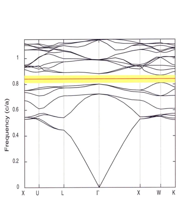
Fig. 2-2 shows the bandstructure of a system with a shrunk silica sphere of radius 0.35a. The bands for the bulk structure were calculated using a basis set ranging from (8,8,8) to (256,256,256), and (16,16,16) was found to be effectively converged. The defect band was calculated by introducing the defect into the system and performing the calculation with a 3x3x3 supercell and a basis set of (48,48,48). A supercell calculation was required in this case because the presence of the defect reduced the periodicity of the structure, and resulted in an increase of the size of the repeating cell. Ideally, we would use an isolated defect in an otherwise periodic crystal, but it turns out that having a periodic system simplifies the calculations enormously, as it allows us to impose periodic boundary conditions and apply Bloch's theorem. The choice of the size of the supercell involves striking a balance between preventing excessive coupling between defects in adjacent supercells (this is equivalent to requiring a high
Q cavity), and computation time. The first consideration leads us to increase the size of the supercell while the second leads us to decrease it. It was found that 3x3x3 gave good results for bandstructure calculations without incurring unacceptably long computation times. We see from the figure that the presence of the defect pulled down some of the upper bands to the middle of the gap while maintaining the overall
0.8
O
0.6
n
0.4
L.0.2
0X U
F
X
W
K
Figure 2-2: (Color) Bandstructure of photonic crystal with point defect mode. Defect calculation performed with 3x3x3 supercell, with a (48,48,48) basis set, for shrunk silica sphere radius of 0.35a. The 3x3x3 supercell calculation for the defect produced bandstructure with multiple folding of bands, and as such the band diagram for that calculation is not edifying to show. The most important result from that calculation, namely, the defect state frequency, was extracted, and this piece of information was incorporated into the above non-supercell bandstructure.