Publisher’s version / Version de l'éditeur:
Vous avez des questions? Nous pouvons vous aider. Pour communiquer directement avec un auteur, consultez la
première page de la revue dans laquelle son article a été publié afin de trouver ses coordonnées. Si vous n’arrivez pas à les repérer, communiquez avec nous à [email protected].
Questions? Contact the NRC Publications Archive team at
[email protected]. If you wish to email the authors directly, please see the first page of the publication for their contact information.
https://publications-cnrc.canada.ca/fra/droits
L’accès à ce site Web et l’utilisation de son contenu sont assujettis aux conditions présentées dans le site LISEZ CES CONDITIONS ATTENTIVEMENT AVANT D’UTILISER CE SITE WEB.
Physical Review. B, Condensed Matter and Materials Physics, 59, 23, 1999
READ THESE TERMS AND CONDITIONS CAREFULLY BEFORE USING THIS WEBSITE.
https://nrc-publications.canada.ca/eng/copyright
NRC Publications Archive Record / Notice des Archives des publications du CNRC :
https://nrc-publications.canada.ca/eng/view/object/?id=f080bb60-3adf-4958-9356-1b6c3edf897f
https://publications-cnrc.canada.ca/fra/voir/objet/?id=f080bb60-3adf-4958-9356-1b6c3edf897f
NRC Publications Archive
Archives des publications du CNRC
This publication could be one of several versions: author’s original, accepted manuscript or the publisher’s version. / La version de cette publication peut être l’une des suivantes : la version prépublication de l’auteur, la version acceptée du manuscrit ou la version de l’éditeur.
For the publisher’s version, please access the DOI link below./ Pour consulter la version de l’éditeur, utilisez le lien DOI ci-dessous.
https://doi.org/10.1103/PhysRevB.59.15368
Access and use of this website and the material on it are subject to the Terms and Conditions set forth at
Manipulating the energy levels of semiconductor quantum dots
Fafard, S.; Wasilewski, Z. R.; Ni. Allen, C.; Picard, D.; Spanner, M.;
McCaffrey, J.; Piva, P. G.
Manipulating the energy levels of semiconductor quantum dots
S. Fafard,*Z. R. Wasilewski, C. Ni. Allen, D. Picard, M. Spanner, J. P. McCaffrey,and P. G. Piva
Institute for Microstructural Sciences, National Research Council, Ottawa, Ontario, Canada, K1A 0R6 ~Received 19 November 1998!
Artificial atoms with up to five well-defined electronic shells are fabricated using self-assembled quantum dots ~QD’s! grown by molecular-beam epitaxy. State-filling spectroscopy of the zero-dimensional transitions between confined electrons and holes demonstrates that the energy levels are readily tunable. One to five confined levels, with an interlevel energy spacing between 25 and 90 meV, are obtained by adjusting the growth temperature or with post growth annealings. The uniformity and reproducibility of InAs/GaAs QD’s are optimized by adjusting growth parameters affecting the evolution and the equilibrium shape of the QD’s: the amount of strained material deposited, and the annealing time following the InAs deposition. Well-defined excited states are also obtained with stacked layers of vertically self-assembled QD’s.
@S0163-1829~99!00124-1#
The prospect of fabricating artificial atoms with tailored properties has fascinated researchers for a long time,1 and stimulated contemporary nanostructure studies. A significant breakthrough occurred five years ago with the development of semiconductor self-assembled quantum dots ~QD’s!.2The small size of these QD’s permitted the demonstration of sev-eral of the expected zero-dimensional properties in a strong quantum confinement regime. These included the discrete density of states with large intersublevel energy spacings, as observed with selective photoluminescence and photolumi-nescence excitation3or with magnetocapacitance,4as well as the evidence of the single QD sharp lines5–8 with their temperature-independent behaviors.9 Also, the structural quality attained permitted a demonstration of high-performance devices such as semiconductor QD lasers.10–17 However, the systematic fabrication of QD structures which would have well-defined excited-state transitions, like an ar-tificial atom, and energy levels which could be manipulated at will, has remained illusive so far. Indeed, the literature reports some observations of excited states in self-assembled QD’s,18–20,11but the reproducibility of such samples and the controlling and tailoring of the shell structure remain to be demonstrated. Such a control will be necessary to understand better the energy relaxation mechanisms of carriers from ex-cited states, and also to fabricate detectors and emitters based on intersublevel transitions in zero-dimensional systems.
In this paper, we show that a combination of detailed studies of the growth kinetics with specific growth sequences leads to an additional degree of size and shape engineering, giving a much improved uniformity of the macroscopic en-sembles of QD’s, with well-resolved electronic shells. The study clearly identifies the key parameters to be controlled: a precise amount of strain material deposited with a low in-plane coverage of QD’s, an anneal time which together with the deposition rate allows the QD’s to evolve to the desired size and uniformity, a growth temperature which yields QD’s with the desired intersublevel energy spacing, and an indium-flush technique which cycles the temperature during the overgrowth of the QD’s to engineer the size and shape of the QD’s and to tailor their intersublevel energy spacings.
The results presented here concentrate on the binary InAs/ GaAs semiconductor system grown on ~100! GaAs sub-strates which emits at l;1mm, but the conclusions can be extended to other material systems such as AlxIn12xAs/AlyGa12yAs ~visible-red emission!,21
InxGa12xAs/AlyGa12yAs ~near-infrared emission!, and
InAs/InxAl12xGaAs/InP ~emission around 1.5 mm!.22 The
layers are grown in a modified V80H molecular-beam-epitaxy system using a nominal As2 molecular flux of 4 31014cm2.23The surface temperature was monitored with a calibrated optical pyrometer. The QD energy levels are probed with state-filling spectroscopy obtained with the pho-toluminescence excited at an energy above the band gap of the barrier material. Various excitation intensities between a fraction of W/cm2to a few kW/cm2are used progressively to reveal the saturation of the lowest energy levels and the emergence of the excited-state emission spectra of many car-riers for higher excitations.18,24
Figure 1 shows state-filling spectroscopy for four differ-ent InAs/GaAs QD samples, and illustrates how the elec-tronic shell structure can be tuned by adjusting the substrate temperature during the formation of the QD’s. Larger QD’s with smaller intersublevel energy spacings are obtained at higher growth temperatures:25 the photoluminescence spec-tra, excited at various intensities, are shown in Fig. 1 for Tgrowth5535 °C ~a!, Tgrowth5515 °C ~b!, Tgrowth5500 °C ~c!,
and Tgrowth;480 °C ~d!. The measured intersublevel energy
spacings are 57, 65, 75, and 90 meV, respectively. This dem-onstrates that the size of the QD’s can be used to control the intersublevel energy spacing between 57 and 90 meV in a simple step during growth. It should be noted, however, that the size is not the only parameter which is modified when changing the substrate temperature. For example, in Fig. 1 the larger intersublevel energy spacings ~tight lateral con-finement! are associated with the QD’s emitting at lower energies, and are obtained by growing at lower substrate temperatures, and therefore are less affected by the possibil-ity of intermixing during growth as will be shown below.
Our control of the growth allows one to grow such uni-form QD’s reproducibly from sample to sample, and also
PRB 59
maintain uniformity, in structures possessing multiple QD layers. The uniformity is readily ascertained. For example, in Fig. 1~b!, the photoluminescence spectra for a single layer of InAs/GaAs QD’s reveal an inhomogeneous broadening of the ground state (n51) as small as 34 meV, displaying four well-resolved excited-state peaks (n52 – 5). These transi-tions originate from shell structures similar to the atomic orbitals S, P, D, F, and G, with the main difference being that here the binding energy of these artificial atoms is ;0.5 eV, with an adjustable intersublevel energy spacing of tens of meV. Comparatively, the hydrogen binding energy is 13.6 eV, and the S- P interlevel energy spacing is ;10 eV. The shells of the QD’s are progressively populated by increasing the number of photocarriers with the photoluminescence ex-citation intensity, as seen here with the state-filling spectros-copy. For such photoexcitation, both electrons and holes are simultaneously present. Alternatively, free carriers can be provided by growing modulation-doped QD heterostructures, where the electrons are provided by dopant atoms places in the barrier material. The amount of deposited InAs required to achieve well-defined electronic shells varies for the differ-ent substrate temperatures. For these InAs/GaAs QD’s, 2.12
ML is required for Tgrowth5535 °C, 1.91 ML for
Tgrowth5515 °C, and 1.84 ML for Tgrowth5500 °C. The
amount of QD material required is dictated by the higher indium desorption rates at more elevated growth tempera-tures, and the kinetic suppression of the island formation at lower growth temperatures.
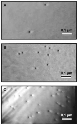
The amount of QD material deposited is critical, and therefore has to be precisely determined. From previous studies, it is known that the onset of the spontaneous island-ing in the Stranski-Krastanow growth mode for InAs/GaAs occurs at about 1.6 ML.26 For self-assembled QD’s by molecular-beam epitaxy, it is common practice to monitor the reflection high-energy electron diffraction pattern during growth to help determine the critical thickness. However, for accurate growth and to obtain uniform QD’s with well-defined electronic shells reproducibly we found it is best to perform a detailed study of the QD evolution27 for a speci-fied calibrated growth rate. With molecular-beam epitaxy, this is most effectively achieved by growing on a stationary 3-in. wafer. Because of the spatial anisotropy in the indium flux due the angle of the cell relative to the wafer, the result-ing growth gives a complete picture of the evolution of the QD’s with indium coverage. All the other samples are grown using a substrate rotation to obtain uniformity throughout the wafers. The results of such a study shows an evolution from a simple wetting layer to high-density dislocated QD’s, with the other growth parameters optimized ~Fig. 2!. To obtain uniform QD’s with well-defined electronic shells, the QD density has to be kept low ~below 100 QD’s permm2!, as can be seen in Fig. 2~a!. For coverages of 1.8 ML or smaller, only a wetting layer photoluminescence peak is observed due to the formation of the thin InAs quantum well which pre-cedes the spontaneous island formation. As the coverage in-creases, the amplitude of the wetting layer peak decreases simultaneously with the increase of the QD peaks due to a higher density of QD’s. This is confirmed with transmission electron microscope images: Fig. 3 shows the structural evo-lution of the QD’s of Fig. 2 for the three different InAs coverages of 1.89 ML @Fig. 3~A!#, 1.91 ML @Fig. 3~B!#, and 1.96 ML @Fig. 3~C!#. The transmission electron microscope analysis reveals a density of 8 QD/mm2, 32 QD/mm2, and 90 QD/mm2for these respective coverages, with approximately constant mean QD diameters of ;20 nm. This suggests that the progressive shift of the ground state observed in Fig. 2~A! is not likely caused by a change in the QD size, but is rather an effect of the lateral strain fields from the adjacent QD’s, which also affect the excited-state energy levels. A maximum blueshift of the ground state of ;60 meV is ob-tained when the coverage is increased from 1.83 to ;2.0 ML as can be seen in Fig. 2~b!. In addition to the increased den-sity of strain fields, the observed blueshift could also be ex-plained in part if there is some incorporation of Ga from the barrier into the QD’s, and that the presence of more InAs nucleation sites favors to a certain extent the diffusion of more Ga toward the QD’s in the capping procedure, thus forcing more Ga incorporation into the QD’s as the density of islands is increased.
For denser coverage, little excited-state structure can be resolved. As the lateral separation between the QD’s de-creases with an increasing coverage, the wave functions from adjacent QD’s start to overlap. This effect is first observed
FIG. 1. Tuning of the intersublevel energy spacing with the substrate temperature during the growth of InAs/GaAs QD’s. Larger QD’s with smaller intersublevel energy spacings are ob-tained at higher temperatures: ~a! Shows Tgrowth5535 °C, ~b!
Tgrowth5515 °C, ~c! Tgrowth5500 °C, ~d! Tgrowth;480 °C, giving an
intersublevel energy spacings adjustable between 57 and 90 meV. The state-filling spectroscopy is obtained with the photolumines-cence at 77 K, with the highest excitation of a few kW/cm2above the barrier energy.
with the excited states, which become more delocalized due to the finite confining potential. The amplitude of the photo-luminescence decreases for the highest coverages of Fig. 2~b!, where the higher QD density increases the probability of island coalescence. This leads to large local strains and their release via the generation of dislocations which serve as effective channels for nonradiative carrier recombinations. The QD evolution study revealed that an optimum coverage is obtained when the state-filling spectroscopy displays all the confined QD states in photoluminescence, as well as the wetting layer recombination which is unambiguously as-signed from such an experiment.
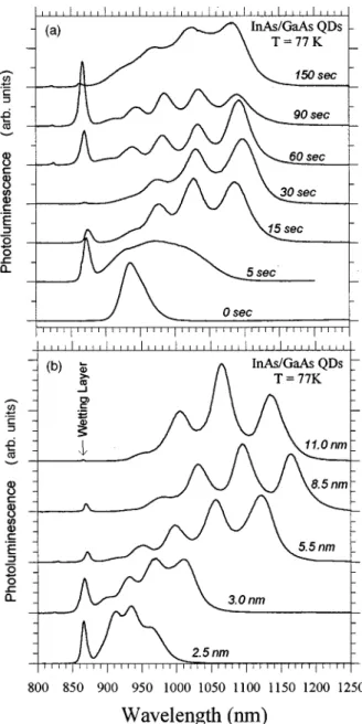
Figure 4~a! shows the state-filling spectroscopy, demon-strating the evolution of the InAs/GaAs QD’s with an anneal
time between 0 and 150 s. The anneal time follows the depo-sition of the optimum 1.9 ML of InAs grown in 27 s at 515 °C. During the anneal time, the growth is interrupted under nominal arsenic flux. The photoluminescence spectra indicate that without an anneal time, QD’s emitting at short wavelengths are obtained, with a ground-state transition ergy only ;100 meV below the wetting layer emission en-ergy. It can be deduced that for such QD’s only one bound electron and hole state is obtained. This suggests that those QD’s are very small, and/or that when the InAs is quickly covered with GaAs, Ga incorporation is more likely, thus reducing the confining potential and blueshifting the emis-sion. It is also clear that at our InAs deposition rate of 0.02 nm/s the QD formation is strongly kinetically limited with no anneal time. Indeed, a remarkable evolution of the QD’s is observed in the first 15 s of anneal: the 5-s sample suggests larger QD’s with excited-state transitions which started de-veloping, and the 15-s sample already displays well-defined excited states. The best uniformity in the QD ensemble is obtained for an anneal time of about 60 s; therefore, this annealing time was chosen for the growth of most of the other samples discussed here. For longer anneal times, a slight degradation in the uniformity is observed. The indium desorption rate is small for the growth temperature used here, but for the longer anneal times it can contribute to the ob-served degradation of the uniformity.
FIG. 2. Evolution of the QD’s with the amount of InAs depos-ited for Tgrowth;480 °C, with coverage between 1.81 and 1.97 ML
in ~a!, and with coverage between 1.90 and 2.28 ML in ~b!. The state-filling spectroscopy is obtained with the photoluminescence at 77 K, excited with a few kW/cm2 above the barrier energy. For clarity, each photoluminescence spectrum is offset to the number on the vertical axis which corresponds to the coverage in monolayers for that spectrum.
FIG. 3. Plan view transmission electron microscope images of the evolution of the InAs/GaAs QD’s of Fig. 2, taken at three dif-ferent InAs coverages: ~A! is for 1.89 ML giving a density of 8 QD/mm2; ~B! is for 1.91 ML giving a density of 32 QD/mm2; and
~C! is for 1.96 ML giving a density of 90 QD/mm2. In all cases the mean QD diameter remains ;20 nm.
In this section, we demonstrate a growth procedure which can be used to improve significantly the uniformity of the vertically self-assembled stacked QD’s, and to size and shape engineer the QD’s in the case of single-layer samples. The main difference compared to the typical growth se-quence is the use of an indium-flush step,28 which removes all surface resident indium at some position during the over-growth of the GaAs cap layer. Figure 4~b! shows the impact on the photoluminescence spectra of such size and shape engineering of the QD’s. The tuning of the intersublevel
en-ergy spacing was achieved here with an indium flush ex-ecuted after the deposition of thin GaAs caps between 2.5 and 11.0 nm. The InAs/GaAs QD’s are formed by depositing 1.9 ML of InAs over 27 s at 515 °C, with an anneal of 60 s @see Fig. 4~a!#. During the indium flush, the growth is inter-rupted and the substrate temperature rapidly raised to ;610 °C to eliminate any indium from the growth front. The wafer temperature can then be ramped back to 515 °C for the case of stacks with multiple layers of QD’s, or kept at the higher temperature during the completion of the GaAs cap, to a thickness of 100 nm in all cases shown here in Fig. 4~b! for single-layer samples. For samples with the indium flush performed after the deposition of a GaAs thickness thinner than 2.0 nm, most of the InAs is evaporated. This can be deduced from the photoluminescence spectra ~not shown!, which display little emission at energies lower than the wet-ting layer transition. This is also corroborated with in situ desorption mass spectrometry studies using a quadrupole mass spectrometer.28 For an indium flush executed after thicknesses between 2.5 and about 5.5 nm, the QD’s can be continuously adjusted from having a more disklike shape to a more standard lens shape. The total number of bound zero-dimensional states changes from three for the sample indium flushed at 2.5 nm to five for the sample indium flushed at 5.5 nm, as can be seen in Fig. 4~b!. At the same time, the inter-sublevel energy spacing is tuned from ;25 to ;65 meV. For the samples indium flushed with GaAs thicknesses larger than about 5.5 nm, little InAs is removed and the intersub-level spacing remains about the same, but the energy-intersub-level positions shift slightly due to the changes in the potential caused by the combined effects of QD intermixing ~see be-low!, and indium segregation in the barrier. The indium-flush procedure is very reproducible from sample to sample, and the QD energy levels shift in a smooth and predictable way. The indium-flush technique is therefore very suitable to gain an additional degree of size and shape engineering of the self-assembled QD’s in single or multiple layers.
Post-growth tuning of the electronic shell structure can also be achieved using QD intermixing.29 For example, Fig. 5 shows the results for a rapid thermal annealing of 30 s which was performed at the indicated temperatures between 700 and 900 °C. The original InAs/GaAs QD’s were grown with 1.9 ML of InAs deposited in 27 s at 515 °C, with an anneal of 60 s @see Fig. 4~a!#, and an indium flush at 5.0 nm @see Fig. 4~b!#. The post-growth QD intermixing has two main remarkable effects. It further narrows the emission dis-tribution of the QD’s, as can be deduced by the photolumi-nescence linewidths in Fig. 5, and it reduces the intersublevel energy spacing. Here the QD’s can be continuously adjusted from five confined zero-dimensional states with an intersub-level energy spacing of ;65 meV, to four confined zero-dimensional states with an intersublevel energy spacing of ;25 meV, and with a blueshift of the ground state of ;200 meV for the 900 °C rapid thermal annealing. The QD blue-shift is remarkably enhanced compared to its two-dimensional wetting layer counterpart, which only shifted by 13 meV while the QD’s shifted by 200 meV. The post-growth QD intermixing can therefore be used to achieve a targeted intersublevel energy spacing ~relative to phonon en-ergies, for example!, or to blueshift integrated optoelectronic devices selectively.
FIG. 4. Size and shape engineering of the QD’s, and tuning of the intersublevel energy spacing: the state-filling spectroscopy, show the evolution of the InAs/GaAs QD’s. ~a! An anneal time, between 0 and 150 s following the deposition of 1.9 ML of InAs grown in 27 s at 515 °C. ~b! An indium flush executed after the deposition of thin GaAs caps between 2.5 and 11.0 nm. The InAs/ GaAs QD’s are made with 1.9 ML of InAs grown in 27 s at 515 °C, with an anneal of 60 s. During the indium flush, the growth is interrupted and the substrate temperature is raised to ;610 °C, after which the GaAs cap is completed to a thickness of 100 nm in all cases. The photoluminescence is excited above the barrier energy with a few kW/cm2.
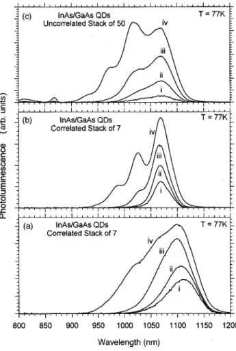
For certain devices such as QD laser diodes, it is desirable to grow multiple layers of QD’s. Here we demonstrate that stacked QD’s displaying vertical self-alignment can also be optimized, and display well-defined electronic shells. In the case of stacks where the spacer between the QD layers is small enough to lead to vertical self-alignment ~,;20 nm! but thick enough to have little wave-function coupling be-tween QD’s in adjacent layers ~.;8 nm!, the vertical self-alignment commonly leads to a reduced QD uniformity and consequently to larger emission linewidths. This is illustrated in Fig. 6~a! for a correlated stack of seven layers separated by 10 nm of GaAs, grown at 515 °C without an indium flush. No well-defined excited-state transitions can be observed be-cause of the change in the QD average size from one layer to the next, as observed from the transmission electron micro-scope images.17,30–32 This uniformity problem with corre-lated stacks can be circumvented using the indium-flush technique described above. This is illustrated in Fig. 6~B!, which is for a sample grown under the same conditions as the one of Fig. 6~a! but with an indium flush executed at 5.0 nm in the middle of the GaAs barrier. The number of stacked layers can be further increased while preserving the well-resolved electronic shell structure. For example, Fig. 6~c! shows the case of a vertically uncorrelated stack of 50 layers,
separated by 30 nm of GaAs, grown at 515 °C with an in-dium flush executed at 5.0 nm.
By studying and controlling the growth kinetics ~precise amount of material deposited, anneal time, growth tempera-ture, and indium-flush procedure during the overgrowth!, very good reproducibility has been achieved with samples grown several months apart. This size and shape engineering and this control of the QD’s permit one to manipulate the energy levels of such man-made atoms freely, and will allow the study of the physics of tunneling between coupled QD’s ~artificial molecules!, of recombination in charged QD’s, and of carrier injection and lasing in QD’s with well-defined ex-cited states.
*Electronic address: [email protected]
1Y. Arakawa and H. Sakaki, Appl. Phys. Lett. 40, 939 ~1982!; H.
Sakaki, Jpn. J. Appl. Phys. 28, L314 ~1989!; Surf. Sci. 267, 623 ~1992!.
2D. Leonard, M. Krishnamurthy, C. M. Reaves, S. P. Denbaars,
and P. M. Petroff, Appl. Phys. Lett. 63, 3202 ~1993!; D. Le-onard, S. Fafard, K. Pond, Y. H. Zhang, J. M. Merz, and P. M. Petroff, J. Vac. Sci. Technol. B 12, 2516 ~1994!; D. Leonard, M.
Krishnamurthy, S. Fafard, J. M. Merz, and P. M. Petroff, J. Vac. Sci. Technol. B 12, 1063 ~1994!.
3S. Fafard, D. Leonard, J. M. Merz, and P. M. Petroff, Appl. Phys.
Lett. 65, 1388 ~1994!.
4H. Drexler, D. Leonard, W. Hansen, J. P. Kotthaus, and P. M.
Petroff, Phys. Rev. Lett. 73, 2252 ~1994!; K. H. Schmidt, G. Medeiros-Ribeiro, and P. M. Petroff, Phys. Rev. B 58, 3597 ~1998!.
FIG. 5. Post growth tuning of the intersublevel energy spacing using QD intermixing. A Rapid thermal anneal of 30 s was per-formed at the indicated temperatures. The original InAs/GaAs QD’s were grown with 1.9 ML of InAs grown in 27 s at 515 °C, with an anneal of 60 s @see Fig. 4~a!#, and an indium flush at 5.0 nm @see Fig. 4~b!#. The state-filling spectroscopy is obtained with the pho-toluminescence at 77 K, excited with a few kW/cm2 above the barrier energy.
FIG. 6. State-filling spectroscopy of stacks of InAs/GaAs QD’s displaying well-defined electronic shells due to the good QD uni-formity. Photoluminescence at 77 K for various excitation intensi-ties for a correlated stack of seven layers separated by 10 nm of GaAs without an indium flush in ~a!, for a correlated stack of seven layers separated by 10 nm of GaAs with an indium flush executed at 5.0 nm in ~b!, and for an uncorrelated stack of 50 layers separated by 30 nm of GaAs in ~c!.
5S. Fafard, R. Leon, D. Leonard, J. L. Merz, and P. M. Petroff,
Phys. Rev. B 50, 8086 ~1994!.
6J. Y. Marzin, J. M. Ge´rald, A. Izrael, D. Barrier, and G. Bastard,
Phys. Rev. Lett. 73, 716 ~1994!.
7Y. Toda, S. Shinomori, K. Suzuki, and Y. Arakawa, Appl. Phys.
Lett. 73, 517 ~1998!.
8L. Landin, M. S. Miller, M. E. Pistol, C. E. Pryor, and L.
Sam-uelson, Science 280, 262 ~1998!.
9G. Wang, S. Fafard, D. Leonard, J. E. Bowers, J. M. Merz, and P.
M. Petroff, Appl. Phys. Lett. 64, 2815 ~1994!; S. Fafard, S. Raymond, G. Wang, R. Leon, D. Leonard, S. Charbonneau, J. L. Merz, P. M. Petroff, and J. E. Bowers, Surf. Sci. 361, 778 ~1996!.
10S. Fafard, Photonics Spectra 31, 160 ~1997!; S. Fafard, K. Hinzer,
S. Raymond, M. Dion, J. McCaffrey, Y. Feng, and S. Charbon-neau, Science 274, 1350 ~1996!.
11N. N. Ledentsov, V. M. Ustinov, V. A. Shchukin, P. S. Kop’ev,
Zh. I. Alferov, and D. Bimberg, Semiconductors 32, 343 ~1998!.
12R. Mirin, A. Gossard, and J. Bowers, Electron. Lett. 32, 1732
~1996!.
13Q. Xie, A. Kalburge, P. Chen, and A. Madhukar, IEEE Photonics
Technol. Lett. 8, 965 ~1996!.
14H. Shoji et al., IEEE Photonics Technol. Lett. 12, 1385 ~1995!;
H. Shoji, Y. Nakata, K. Mukai, Y. Sugiyama, M. Sugawara, N. Yokoyama, and H. Ishikawa, Jpn. J. Appl. Phys., Part 2 35, L903 ~1996!; Electron. Lett. 32, 2023 ~1996!.
15H. Saito, K. Nishi, I. Ogura, S. Sugou, and Y. Sugimoto, Appl.
Phys. Lett. 69, 3140 ~1996!.
16K. Kamath, P. Bhattacharya, T. Sosnowski, T. Norris, and J.
Phil-lips, Electron. Lett. 32, 1374 ~1996!.
17S. Fafard, K. Hinzer, A. J. SpringThorpe, Y. Feng, J. McCaffrey,
S. Charbonneau, and E. M. Griswold, Mater. Sci. Eng. 51, 114 ~1998!.
18S. Fafard, R. Leon, D. Leonard, J. L. Merz, and P. M. Petroff,
Phys. Rev. B 52, 5752 ~1995!.
19K. Mukai, N. Ohtsuka, H. Shoji, and M. Sugawara, Appl. Phys.
Lett. 68, 3013 ~1996!.
20Y. Sugiyama, Y. Nakata, T. Futatsugi, M. Sugawara, Y. Awano,
and N. Yokoyama, Jpn. J. Appl. Phys. 36, L158 ~1997!.
21R. Leon, P. M. Petroff, D. Leonard, and S. Fafard, Science 267,
1966 ~1995!; R. Leon, S. Fafard, D. Leonard, J. L. Merz, and P. M. Petroff, Appl. Phys. Lett. 67, 521 ~1995!.
22S. Fafard, Z. Wasilewski, J. McCaffrey, S. Raymond, and S.
Charbonneau, Appl. Phys. Lett. 68, 991 ~1996!; S. Fafard, J. McCaffrey, Y. Feng, C. Ni Allen, H. Marchand, L. Isnard, P. Desjardins, S. Guillon, and R. A. Masut, Proc. SPIE 3491, 272 ~1998!.
23Z. R. Wasilewski, S. J. Rolfe, and R. A. Wilson, J. Cryst. Growth
175/176, 1270 ~1997!.
24S. Raymond, P. Hawrylak, C. Gould, S. Fafard, A. Sachrajda, M.
Potemski, A. Wojs, S. Charbonneau, D. Leonard, P. M. Petroff, and J. L. Merz, Solid State Commun. 101, 883 ~1997!; A. Wojs and P. Hawrylak, ibid. 100, 487 ~1996!; A. Wojs, P. Hawrylak, S. Fafard, and L. Jacak, Phys. Rev. B 54, 5604 ~1996!; S. Ray-mond, X. Guo, J. L. Merz, and S. Fafard, Phys. Rev. B 59, 7624 ~1999!.
25R. Leon, C. Lobo, A. Clark, R. Bozek, A. Wysmolek, A.
Kurpiewski, and M. Kaminska, J. Appl. Phys. 84, 248 ~1998!.
26D. Leonard, K. Pond, and P. M. Petroff, Phys. Rev. B 50, 11 687
~1994!.
27R. Leon and S. Fafard, Phys. Rev. B 58, R1726 ~1998!. 28Z. R. Wasilewski, S. Fafard, and J. P. McCaffrey, J. Crys. Growth
~to be published!.
29R. Leon, S. Fafard, P. G. Piva, S. Ruvimov, and Z.
Liliental-Weber, Phys. Rev. B 58, R4262 ~1998!.
30Q. Xie, A. Madhukar, P. Chen, and N. P. Kobayashi, Phys. Rev.
Lett. 75, 2542 ~1995!.
31L. Goldstein, F. Glas, J. Y. Marzin, M. N. Charasse, and G.
LeRoux, Appl. Phys. Lett. 47, 1099 ~1985!.
32G. S. Solomon, J. A. Trezza, A. F. Marshall, and J. J. S. Harris,
Phys. Rev. Lett. 76, 952 ~1996!.