RESEARCH OUTPUTS / RÉSULTATS DE RECHERCHE
Author(s) - Auteur(s) :
Publication date - Date de publication :
Permanent link - Permalien :
Rights / License - Licence de droit d’auteur :
Bibliothèque Universitaire Moretus Plantin
Institutional Repository - Research Portal
Dépôt Institutionnel - Portail de la Recherche
researchportal.unamur.be
University of Namur
Toward the use of CVD-grown MoS2 nanosheets as field-emission source
Deokar, Geetanjali; Rajput, Nitul; Lie, Junjie ; Deepak, Francis Leonard; Ou-Yang, Wei;
Reckinger, Nicolas; Bittencourt, Carla; Colomer, Jean-François; Jouiad, Mustapha
Published in:
Beilstein Journal of Nanotechnology
DOI:
10.3762/bjnano.9.160
Publication date:
2018
Document Version
Publisher's PDF, also known as Version of record
Link to publication
Citation for pulished version (HARVARD):
Deokar, G, Rajput, N, Lie, J, Deepak, FL, Ou-Yang, W, Reckinger, N, Bittencourt, C, Colomer, J-F & Jouiad, M
2018, 'Toward the use of CVD-grown MoS2 nanosheets as field-emission source', Beilstein Journal of
Nanotechnology, vol. 9, no. 1, pp. 1686-1694. https://doi.org/10.3762/bjnano.9.160
General rights
Copyright and moral rights for the publications made accessible in the public portal are retained by the authors and/or other copyright owners and it is a condition of accessing publications that users recognise and abide by the legal requirements associated with these rights. • Users may download and print one copy of any publication from the public portal for the purpose of private study or research. • You may not further distribute the material or use it for any profit-making activity or commercial gain
• You may freely distribute the URL identifying the publication in the public portal ? Take down policy
If you believe that this document breaches copyright please contact us providing details, and we will remove access to the work immediately and investigate your claim.
as field-emission source
Geetanjali Deokar
*1,2, Nitul S. Rajput
1, Junjie Li
3, Francis Leonard Deepak
3,
Wei Ou-Yang
*4, Nicolas Reckinger
2, Carla Bittencourt
5, Jean-Francois Colomer
2and Mustapha Jouiad
*1Full Research Paper
Open AccessAddress:
1Department of Mechanical and Materials Engineering, Masdar Institute of Science and Technology, A part of Khalifa University of Science and Technology, 54224, Abu Dhabi, United Arab Emirates,
2Research Group on Carbon Nanostructures (CARBONNAGe), University of Namur, 61 Rue de Bruxelles, 5000 Namur, Belgium,
3Department of Advanced Electron Microscopy, Imaging and Spectroscopy, International Iberian Nanotechnology Laboratory (INL), Avenida Mestre Jose Veiga, Braga 4715-330, Portugal, 4Engineering Research Center for Nanophotonics & Advanced Instrument, Ministry of Education, School of Physics and Materials Science, East China Normal University, 3663 North Zhongshan Road, Shanghai 200062, China and 5Chimie des Interactions Plasma-Surface (ChIPS), CIRMAP, Research Institute for Materials Science and Engineering, University of Mons, Mons, Belgium
Email:
Geetanjali Deokar* - [email protected]; Wei Ou-Yang* [email protected]; Mustapha Jouiad* [email protected]
* Corresponding author
Keywords:
chemical vapor deposition (CVD); field emission; molybdenum disulfide (MoS2); nanosheets; sulfurization; transmission electron microscopy (TEM) Beilstein J. Nanotechnol. 2018, 9, 1686–1694. doi:10.3762/bjnano.9.160 Received: 17 November 2017 Accepted: 11 May 2018 Published: 07 June 2018
Associate Editor: N. Motta
© 2018 Deokar et al.; licensee Beilstein-Institut. License and terms: see end of document.
Abstract
Densely populated edge-terminated vertically aligned two-dimensional MoS2 nanosheets (NSs) with thicknesses ranging from 5 to 20 nm were directly synthesized on Mo films deposited on SiO2 by sulfurization. The quality of the obtained NSs was analyzed by scanning electron and transmission electron microscopy, and Raman and X-ray photoelectron spectroscopy. The as-grown NSs were then successfully transferred to the substrates using a wet chemical etching method. The transferred NSs sample showed excellent field-emission properties. A low turn-on field of 3.1 V/μm at a current density of 10 µA/cm2 was measured. The low turn-on field is attributed to the morphology of the NSs exhibiting vertically aligned sheets of MoS2 with sharp and exposed edges. Our findings show that the fabricated MoS2 NSs could have a great potential as robust high-performance electron-emitter material for various applications such as microelectronics and nanoelectronics, flat-panel displays and electron-microscopy emitter tips.
Beilstein J. Nanotechnol. 2018, 9, 1686–1694.
1687
Introduction
There is a great interest in the development of one- and two-dimensional (1D and 2D) materials for field-emission (FE) based cathodes using various nanostructured materials [1] for applications in displays, X-ray sources and cold-cathode elec-tron sources [2]. 1D and 2D materials such as carbon nanotubes [3], ZnO nanorods [1], LaB6 nanowires [2], SnS2 nanosheets (NSs) [4], vertically aligned graphene [5], WS2 nanotubes [6], MoSe2 nanosheets [7], and MoS2 NSs [8-10] are potential field-emitter candidates. The FE properties depend on the microstruc-ture of the materials, such as morphology, orientation, size and internal or intrinsic features [1]. Among the different morpholo-gies of 1D and 2D materials, vertically aligned nanostructures are considered as good candidates for field emission. Due to their exposed sharp edges, un-stacked morphology and high aspect ratio they are less affected by Joule heating [11]. In the past few years, FE measurements on different MoS2 morpholo-gies, such as horizontally arranged (with a few protruding portions) MoS2 [12], sparsely distributed vertically aligned MoS2 NSs [9], MoS2 nanoflowers [13] and MoS2 nano-heteroarchitectures [14] have been reported. The semicon-ducting MoS2 NSs with exposed edges could significantly en-hance the FE properties [9]. It is well known that the electrical and optical properties of MoS2 are influenced by their size, shape [15,16] and the number of layers [16]. Various methods have been used to synthesize vertically aligned MoS2 NSs: liquid-phase exfoliation [17], hydrothermal synthesis [8] or chemical vapor deposition (CVD) [15,17,18]. CVD is regarded as the most promising method to synthesize high-quality MoS2
with good control over size, shape and morphology [17,19]. So far, relatively few FE measurements on vertically aligned MoS2
NSs [9] and nanoflowers [13] have been reported. Significant challenges still remain in the development of MoS2 nanostruc-tures for large-scale FE devices using a simple, efficient and low-cost production technology with high quality and large quantities. An ideal FE material would have a low work func-tion, aligned arrays of sharp tips, large aspect ratio, high stability and moderate current density, as well as the capability to be placed easily on a conductive substrate [1]. Herein, we report on the FE properties of densely packed and uniformly distributed vertically aligned 2D MoS2 NSs, well adhered to the substrate. These NSs were synthesized by double sulfurization of sputter-deposited Mo films on Si (300 nm SiO2/Si) sub-strates. The FE properties assessment is carried out on the NSs transferred onto a conducting fluorine-tin-oxide (FTO) sub-strate.
Experimental
Sample preparation
The NSs were grown on SiO2/Si substrates via double sulfuriza-tion of a sputter-deposited 50 nm Mo film using an
ambient-pressure CVD technique. Flushing of the quartz tube using Ar gas stream, followed by continuous Ar flow for 1 h was per-formed. This reduces the oxygen content in the reactor prior to the sulfurization process. The growth conditions were taken and improved from our previously reported MoS2 NS synthesis method [18]. In a typical sulfurization process, 220 g sulfur powder was placed at the 40 °C temperature zone and the 850 °C temperature zone (total 440 g) along with the Mo film sample placed at the 850 °C temperature zone in the down-stream of the Ar flow in the quartz tube reactor. In the first sulfurization step of 30 min the S powder was placed at the 800 °C zone. The optimized second sulfurization step was per-formed by inserting the quartz tube in the hot zone of the furnace, such that the S powder placed at 40 °C reaches the 400 °C temperature zone. The sample remained at 850 °C as the quartz reactor was moved over a few centimeters.
Wet chemical transfer
A polymer-assisted wet-chemical method was employed to transfer the MoS2 layer on conducting substrates [20]. A layer of poly(methyl methacrylate) (PMMA), 200 nm thick, was coated onto the surface of the MoS2/SiO2/Si sample surface (PMMA/MoS2/SiO2/Si), then floated on buffered oxide etchant. After leaving it overnight, the silica layer was removed, freeing the PMMA/MoS2 film from the growth substrate (SiO2/Si). The sample was subsequently transferred to deionized water to rinse the chemical etchants. Then, the desired substrate (here, FTO) was used to lift the PMMA/MoS2 out of the water. The sample was then dried overnight to let the water trapped underneath the MoS2 NSs to be removed naturally. Next, the sample was baked at 110 °C for 10 min to improve the uniformity and the adhe-sion to the substrate. Finally, the PMMA was dissolved in ace-tone.
Physical characterization methods
The morphology of sulfurized Mo films on SiO2/Si substrates was characterized using field-emission scanning electron microscopy (FE-SEM) combined with a Helios FEITM
NanoLab 650 focused ion beam (FIB) system. Transmission electron microscopy (TEM) lamella were prepared using the standard FIB lift-out technique described in an earlier report [21]. To have a plane view of the deposited material, the sam-ple was locally capped using FIB-assisted Pt deposition and the cut block was lifted out using an OmniprobeTM. The block was tilted at 90° relative to its original position and mounted onto a TEM grid. The TEM investigations were performed using an image-corrected Titan G2 FEITM system. For selected samples, cross-section TEM analyses were carried out using an aberra-tion-corrected FEITM Titan ChemiSTEM system (equipped with a Cs probe corrector, a high-angle annular dark-field
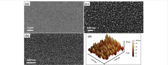
Figure 1: (a–c) Typical field-emission SEM images with different magnifications of MoS2 NSs grown by double sulfurization of a 50 nm Mo film at 850 °C on SiO2/Si substrates; (d) AFM image: 3D image of panel (b) in Figure S1.
imaging (HAADF) detector and a four quadrant Super X energy-dispersive spectroscopy (EDS) detector) operating at 200 kV for imaging and elemental characterization. Roughness and topography of the as-grown MoS2 NSs (before transfer) were examined by atomic force microscope (AFM). The AFM scans were recorded in resonant mode (AppNanoTM made can-tilever with tip radius below 10 nm) with a resonant frequency of 312 kHz. To confirm the layer number of the NSs, micro-Raman spectroscopy was performed using a 473 nm laser at room temperature. X-ray photoelectron spectroscopy (XPS) measurements were performed using a Thermo Fisher Scien-tific K-alpha spectrometer with a 250 μm diameter X-ray spot. The FE properties of the MoS2 NSs film transferred on the conductive FTO glass substrate (Figure 5) were measured using a custom-built conventional diode-type structure over a 1 cm2
area in a chamber under high vacuum (4.0 × 10⁻⁶ mbar). The thin film of MoS2 NSs deposited on the FTO glass substrate served as electron-emission cathode and another piece of conductive FTO glass was used as anode. The distance be-tween the cathode and anode was fixed at 220 µm by using thin glass spacers. The FE current (I) versus the applied voltage (V) was measured using an electrometer (Tianjin Dongwen, China) and a high-voltage direct current power supply. The FE current stability was investigated using a computer-controlled data acquisition system with a certain sampling interval.
Results and Discussion
MoS
2NSs morphology and composition
The continuous and dense distribution of vertically aligned MoS2 NSs on SiO2/Si substrates with a thickness of 5–20 nm can be observed from the representative FE-SEM image shown in Figure 1. An optimized double sulfurization step gives a ho-mogeneous distribution of MoS2 NSs over the entire sample
surface without forming any aggregated crystals. Therefore, unlike in the previous case [20], the growth of micrometer-size crystals (of Mo or MoO3) on the sample surface was not ob-served. The AFM measurements confirm (Figure S1, Support-ing Information File 1) a dense growth of MoS2 NSs. The ob-served root mean square roughness was 8 nm (measured over an area of 2.5 × 2.5 µm2). The 3D image (Figure 1d) confirms a tip-like morphology of the MoS2 NSs, which is believed to pos-sess an important role in the measured FE current (discussed later). It can also be noted that the growth of MoS2 NSs re-ported here is of better quality in terms of homogeneous distri-bution and vertical alignment compared to the previously re-ported MoS2 nanostructures (on which FE studies were per-formed), which were sparsely and randomly distributed [9]. The NSs reported by Kashid et al. have few protruding MoS2 NSs and mostly planar surfaces [12].
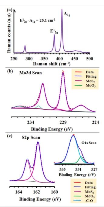
A typical Raman spectrum of the as-synthesized MoS2 NSs, is shown in Figure 2a, indicating the characteristics of the 2H-MoS2 in-plane vibrational mode (E12g) at 383.1 cm−1 and the out-of-plane vibrational mode (A1g) at 408.3 cm−1 [22]. The difference in frequency between the two vibration modes is 25.2 cm−1, which indicates the presence of more than three layers of MoS2 [23]. The chemical state of the as-grown sam-ples was investigated by XPS. The Mo 3d, S 2p and O 1s high-resolution core-level spectrum fits are presented in Figure 2b,c. The corresponding data analysis results are given in Table S1 (Supporting Information File 1). In the high-resolution Mo 3d core-level spectrum fit, the doublet Mo 3d5/2 and Mo 3d3/2
peaks at 228.9 and 232 eV, respectively, are attributed to the formation of MoS2 (Figure 2b) [23,24]. This is further con-firmed by the presence of a shoulder in the S 2s region at 226.2 eV [23]. A very small contribution corresponding to
Beilstein J. Nanotechnol. 2018, 9, 1686–1694.
1689
Figure 2: MoS2 NSs grown by double sulfurization of a 50 nm Mo film at 850 °C on SiO2/Si substrates: (a) typical micro-Raman spectrum; (b) Mo 3d core level and (c) S 2p core level with, in the inset, the O 1s core-level spectrum. The doublet peaks marked with identical color correspond to one phase. More detailed information is summarized in Table S1 (Supporting Information File 1).
MoO3 (Mo6+ oxidation state) phases was also observed (Figure 2b) with Mo 3d5/2 and Mo 3d3/2 component peaks at 232.7 and 235.6 eV, respectively [24]. Additionally, the pres-ence of the main MoS2 phase (corresponding to the observed major peaks) is confirmed by the S 2p core-level spectrum fit presented in Figure 2c, with the S 2p3/2 and S 2p1/2 component peaks appearing at 161.8 and 163 (MoS3) eV (Table S1, Sup-porting Information File 1), respectively, with a spin–orbit energy separation of 1.2 eV corresponding to MoS2 (S2− oxida-tion state) [24]. In the O 1s core-level spectrum (inset of Figure 2c), a small peak corresponding to MoO3 in agreement
with the Mo 3d spectra fitting with a binding energy of 530.2 eV was observed [24,25]. The other peak at 532.3 eV is assigned to O–C bonds [25]. This peak could be explained by the fact that the sample was stored in air for several days before performing the XPS measurements. Thus, the surface-sensitive characterization technique (XPS) shows the dominant presence of the MoS2 phase on the sample surface.
Microstructural analysis of the MoS
2NSs
In Figure 3, plane-view images of as-grown MoS2 NSs are presented. A bright -field TEM image (Figure 3a) indicates the presence of NSs over the entire area. The as-grown NSs, densely packed with very high crystalline quality, can be seen. The fast Fourier transform (FFT) image of Figure 3a is given in Figure 3c. The ring pattern indicates that the NSs are made of MoS2 polycrystals. A high-resolution (HR) TEM image is shown in Figure 3b. The stacking periodicity (the interlayer dis-tance) is found to be around 0.63 nm. The number of layers in a NS is found in the range of 15–20. One should note that the NS thickness cannot be solely determined by plane-view TEM since some layers could be viewed via the bended NSs. Figure 3d is a filtered HRTEM image showing evidence of MoS2 NS stacking defects highlighted by the arrows. These defects are inherent to the fabrication process. This NSs stacking configuration could exhibit interesting properties in membrane technologies such as filtration membranes to remove fouling, heavy metals and chemicals from water by membrane separation as reported elsewhere for graphene nanosheets [26].To investigate further the NSs growth, cross-section TEM mea-surements were performed. The general morphologies of the vertically standing and densely packed MoS2 NSs grown on SiO2/Si substrates can be seen from the low-magnification scan-ning TEM (STEM) image (Figure 4a). The STEM image (Figure 4b) demonstrates that the MoS2 NSs growth occurred perpendicular to the substrate. The height of the NSs ranges from 50 to 70 nm. The corresponding layer is marked with “A” in Figure 4a. Each NS consists of 10 to 20 MoS2 layers. From Figure 4b, detailed structures at the tip of the MoS2 NSs can be observed. It reveals the presence of NSs with exposed edges, which may act as emission sites. The active sites of MoS2 NSs edges are catalytically active and are thus highly preferable as a catalyst surface over the relatively inert MoS2 basal plane [27]. Figure 4c shows the atomic structure of the MoS2 NSs with some edge dislocations (labelled as “T”) along the c-axis. More-over, the interplanar distances are ca. 0.62 and ca. 0.30 nm, cor-responding to the (002) and (004) planes of 2H-MoS2 [18]. However, a slightly higher interplanar distance of 0.63 nm near the edges (in agreement with plane-view TEM) was also ob-served. It indicates that the NSs possess a slightly different lattice parameter due to the crystal confinement at the top end.
Figure 3: MoS2 sample grown by double sulfurization of a 50 nm Mo film at 850 °C on SiO2/Si substrates: (a) Plane-view HRTEM image; (b) high-magnification TEM image; (c) FFT pattern of panel (a); (d) filtered HRTEM image indicating the presence of sheet stacking defects (indicated by orange arrows).
Figure 4: MoS2 sample grown by double sulfurization of a 50 nm Mo film at 850 °C on SiO2/Si substrates: (a) HAADF-STEM image at low magnifica-tion with different observed materials layers marked; (b) TEM image at the interface between the MoS2 NSs and the Pt layer; (c) higher magnification of layer A showing edge dislocation (marked with “T”) in the MoS2 layers; (d) high-magnification HAADF-STEM image at the interface between “A” and “B” from panel (a); (e–g) FFT analysis over the area marked by the dotted squares in panel (d), from top to bottom respectively.
Additionally, the FFT pattern as shown in Figure 4e for the yellow squared area in Figure 4d, confirms well-crystallized MoS2 NSs with the c-axis being normal to the NSs. Between, the vertically aligned MoS2 NSs and the SiO2/Si substrate, a layer (marked with “B” in Figure 4a) containing Mo, S and O (37–55 nm) was detected by EDS (Figure S2, Supporting Infor-mation File 1). This indicates that partial sulfurization of the initial Mo film (50 nm thick) occurred in the entire volume.
Field-emission results
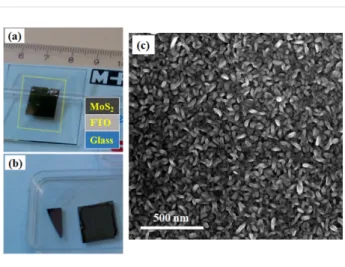
FE measurements on the transferred MoS2 NSs are given in Figure 5. The transferred NSs were checked using SEM (Figure 5c) and Raman spectroscopy (not shown as it is iden-tical to the as-grown NSs). It was thus confirmed that they are of similar quality to that of as-grown NSs. The Fowler–Nord-heim (F–N) equation [28] was modified for a cathode with nanometric field emitters as follows:
Beilstein J. Nanotechnol. 2018, 9, 1686–1694.
1691
Figure 6: (a) Field-emission current density as a function of the electric field for the transferred MoS2 NSs on FTO/glass. The inset shows the corre-sponding FN plot with a linear fitting used for estimating the field-enhancement factor. (b) The long-term field-emission stability for the same sample at the pressure of ca. 10−6 mbar with luminance from the sample.
Figure 5: Photographs of (a) wet chemically transferred MoS2 sample on the FTO/glass substrate, the FTO film on the glass substrate is marked with a yellow dotted square. (b) The remaining square Si sam-ple after being detached from the MoS2 NSs after the buffered oxide etchant. The triangular sample in panel (b) is a piece from the original sample kept for TEM measurements.
(1)
E = U/d, where U is the voltage applied between the flat
cathode and the anode screen and d is the distance in between (220 µm). A and B are constants (A = 1.54 × 10⁻⁶ AeV·V−1,
B = 6.83 × 10⁶ eV−3/2·Vnm−1) that depend on the surface struc-ture. λM is a macroscopic pre-exponential correction factor. UF
(the correction factor) is a particular value of the principal Schottky–Nordheim barrier function U. β is the local electrical field enhancement factor. is the work function of the emitter (considered to be 4.04 eV here [29]). In Figure 6a, the current
density versus electric field (J–E) curve of the transferred MoS2
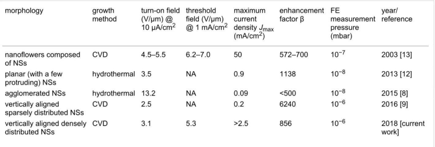
on the FTO sample is displayed. The ln(J/E2) versus 1/E graph of the emission data is shown in the inset of Figure 6a. The linear behavior indicates that FE from the NSs is dominated by the tunneling effect. It can be seen that the density of emission current increases rapidly along with the increasing of the applied electric field (Figure 6a). The turn-on field, defined at a current density of 10 µA/cm2, and the threshold field at 1 mA/cm2, are 3.1 and 5.3 V/µm, respectively. These data are found to be better than the previously reported values for MoS2
nanoflowers [13] or multilayered MoS2 [8,12], and comparable with the vertically aligned MoS2 NSs with ultrathin edges in [9] (Table 1). It has been shown previously that vertically grown 1D nanowires/nanotubes and 2D NSs with atomically thin edges may considerably improve the FE properties, so that vertically standing materials are promising for FE applications [30]. The low turn-on field and threshold field of the MoS2 NSs could be due to their vertically aligned extremely thin edges, forming a nano-tip-like structure (Figure S1, Supporting Infor-mation File 1).
A considerable enhancement in FE can be achieved by tuning the geometrical morphology of the emitter surface and thus it is important to control the surface morphology for producing better field emitters [9,30,31]. The emitter surface is rough for nanomaterials deposited as a planar cathode and, therefore, for a given emission site the applied electric field varies from the local electric field. The ratio of the actual local electric field to the applied average electric field is known as the field-enhance-ment factor. In the present case, the field-enhancefield-enhance-ment factor, commonly used for evaluating FE properties, is calculated from the slope m of the F–N plot (a plot of ln(J/E2) versus 1/E as given in the inset of Figure 6a, using the following equation:
Table 1: Comparison of field-emission properties of MoS2 nanosheets (NSs) produced using different methods. morphology growth method turn-on field (V/μm) @ 10 μA/cm2 threshold field (V/μm) @ 1 mA/cm2 maximum current density Jmax (mA/cm2) enhancement factor β FE measurement pressure (mbar) year/ reference nanoflowers composed of NSs CVD 4.5–5.5 6.2–7.0 50 572–700 10−7 2003 [13]
planar (with a few protruding) NSs hydrothermal 3.5 NA 0.9 1138 10−8 2013 [12] agglomerated NSs hydrothermal 13.2 NA 0.09 <500 10−8 2015 [8] vertically aligned sparsely distributed NSs CVD 2.5 NA 0.2 6240 10−6 2016 [9]
vertically aligned densely distributed NSs
CVD 3.1 5.3 >2.5 856 10−6 2018 [current
work]
(2)
A value of 867 is estimated by linearly fitting the FN plot. This value is indeed higher than that of MoS2 nanoflowers [8,13], and in the range of few-layered MoS2 NS field emitters (β = 1138 for hydrothermally produced MoS2 NSs) [12]. The enhancement factor for our NSs is apparently smaller than the one recently reported on vertically aligned MoS2 NSs (β = 6240 for NSs with ultrathin edges) [9]. However, the electric field re-quired to obtain a high current density of 10 µA/cm2 is much lower for our as-produced NSs as compared to the above report (Table 1). It can be seen that a high current density ≥2.5 mA/cm2 can be achieved (Figure 6a). For the sparsely dis-tributed and ultrathin edge NSs, the current density is only 0.2 mA/cm2 [9]. To obtain high current density from the materi-al is very important for practicmateri-al applications. Thus, as com-pared with previously published horizontally aligned mono-layer or the vertically aligned MoS2 NSs or nanoflowers, the as-produced NSs present a clear advantage in terms of low turn-on field and high current density. It has been demturn-onstrated that film morphology of the cathode greatly influences the field-emission performance and the electrons are easier to be extracted from a film with more exposed edges [32]. Hence, we believe that the tip-like geometry (Figure 1d) and exposed edges (Figure 4) of the MoS2 NSs are enhancing the tunneling probability for electrons in layered nanomaterials. A similar effect has been observed previously in carbon nanotubes [33].
The emission current density versus time plot is shown in Figure 6b. An almost stable (fluctuations between 10 and 20 µA/cm2) emission over a period of 100 min without any measurable degradation can be seen. The densely packed NSs might be playing an important role to achieve high current den-sity and faster heat dissipation, thereby reducing the burning out of active emission sites induced by Joule heating. The as-grown
NSs could also possibly be used as heat dissipating nano-chan-nels in FE or electronic devices [34]. Moreover, the excellent luminance uniformity (except over the film area broken during the transfer process, refer to Figure 5a) of the cathode is demon-strated from the inset in Figure 6b. The stability and luminance results indicate that the as-grown material could be a good emitter in vacuum environments relevant to the industry.
Conclusion
Uniform and continuous MoS2 NSs of 5–20 nm thickness were successfully grown by CVD on SiO2/Si substrates by a double sulfurization step. Micro-Raman and XPS measurements revealed high-quality growth of the vertically aligned NSs. Cross-section TEM measurements revealed that the NSs of 5–20 nm thickness have a height of a few tens of nanometers. AFM measurements showed that the NSs formed a FE nano-tip-like morphology. We have demonstrated that the as-grown NSs can be transferred onto a desired substrate such as conducting FTO/glass employing a wet-chemical transfer process. These NSs show very interesting FE properties at room temperature and in high vacuum (10−6 mbar) as proven by the low turn-on field of 3.1 V/μm and low threshold field of 5.3 V/µm. In future, the as-grown NSs could be potentially used for FE and display device applications.
Supporting Information
Supporting Information File 1
Additional experimental data.
[https://www.beilstein-journals.org/bjnano/content/ supplementary/2190-4286-9-160-S1.pdf]
Acknowledgements
Authors acknowledge Dr. Cyril Aubry for his help in AFM measurement. Part of the research leading to this work received
Beilstein J. Nanotechnol. 2018, 9, 1686–1694.
1693
funding from the European Union Seventh Framework Program under grant agreement No 604391 Graphene Flagship. Francis Leonard Deepak and Junjie Li thank the financial support provi-ded by the N2020: Nanotechnology based functional solutions (NORTE-45-2015-02).
ORCID
®
iDs
Geetanjali Deokar - https://orcid.org/0000-0002-2034-0833 Francis Leonard Deepak - https://orcid.org/0000-0002-3833-1775 Nicolas Reckinger - https://orcid.org/0000-0002-2854-2982 Carla Bittencourt - https://orcid.org/0000-0002-3330-6693 Mustapha Jouiad - https://orcid.org/0000-0002-7587-1500
References
1. Zhai, T.; Li, L.; Ma, Y.; Liao, M.; Wang, X.; Fang, X.; Yao, J.; Bando, Y.; Golberg, D. Chem. Soc. Rev. 2011, 40, 2986–3004.
doi:10.1039/c0cs00126k
2. Zhang, H.; Tang, J.; Yuan, J.; Yamauchi, Y.; Suzuki, T. T.; Shinya, N.; Nakajima, K.; Qin, L.-C. Nat. Nanotechnol. 2016, 11, 273–279. doi:10.1038/nnano.2015.276
3. Fan, S.; Chapline, M. G.; Franklin, N. R.; Tombler, T. W.; Cassell, A. M.; Dai, H. Science 1999, 283, 512–514. doi:10.1126/science.283.5401.512
4. Zhong, H.; Yang, G.; Song, H.; Liao, Q.; Cui, H.; Shen, P.; Wang, C.-X.
J. Phys. Chem. C 2012, 116, 9319–9326. doi:10.1021/jp301024d
5. Malesevic, A.; Kemps, R.; Vanhulsel, A.; Chowdhury, M. P.; Volodin, A.; Haesendonck, C. V. J. Appl. Phys. 2008, 104, 084301. doi:10.1063/1.2999636
6. Viskadouros, G.; Zak, A.; Stylianakis, M.; Kymakis, E.; Tenne, R.; Stratakis, E. Small 2014, 10, 2398–2403. doi:10.1002/smll.201303340 7. Sachin, R. S.; Amit, S. P.; Mahendra, S. P.; Sandesh, R. J.;
Mahendra, A. M.; Dattatray, J. L. Mater. Res. Express 2016, 3, 035003. doi:10.1088/2053-1591/3/3/035003
8. Kashid, R. V.; Joag, P. D.; Thripuranthaka, M.; Rout, C. S.; Late, D. J.; More, M. A. Nanomater. Nanotechnol. 2015, 5, 10. doi:10.5772/60071 9. Li, H.; Wu, H.; Yuan, S.; Qian, H. Sci. Rep. 2016, 6, 21171.
doi:10.1038/srep21171
10. Palacios, E.; Park, S.; Butun, S.; Lauhon, L.; Aydin, K. Appl. Phys. Lett.
2017, 111, 031101. doi:10.1063/1.4993427
11. Bo, Z.; Yang, Y.; Chen, J.; Yu, K.; Yan, J.; Cen, K. Nanoscale 2013, 5, 5180–5204. doi:10.1039/c3nr33449j
12. Kashid, R. V.; Late, D. J.; Chou, S. S.; Huang, Y.-K.; De, M.; Joag, D. S.; More, M. A.; Dravid, V. P. Small 2013, 9, 2730–2734. doi:10.1002/smll.201300002
13. Li, Y. B.; Bando, Y.; Golberg, D. Appl. Phys. Lett. 2003, 82, 1962–1964. doi:10.1063/1.1563307
14. Devan, R. S.; Thakare, V. P.; Antad, V. V.; Chikate, P. R.; Khare, R. T.; More, M. A.; Dhayal, R. S.; Patil, S. I.; Ma, Y.-R.; Schmidt-Mende, L.
ACS Omega 2017, 2, 2925–2934. doi:10.1021/acsomega.7b00345
15. Deokar, G.; Vignaud, D.; Arenal, R.; Louette, P.; Colomer, J.-F.
Nanotechnology 2016, 27, 075604.
doi:10.1088/0957-4484/27/7/075604
16. Eda, G.; Yamaguchi, H.; Voiry, D.; Fujita, T.; Chen, M.; Chhowalla, M.
Nano Lett. 2011, 11, 5111–5116. doi:10.1021/nl201874w
17. Cho, S.-Y.; Kim, S. J.; Lee, Y.; Kim, J.-S.; Jung, W.-B.; Yoo, H.-W.; Kim, J.; Jung, H.-T. ACS Nano 2015, 9, 9314–9321.
doi:10.1021/acsnano.5b04504
18. Deokar, G.; Rajput, N. S.; Vancsó, P.; Ravaux, F.; Jouiad, M.; Vignaud, D.; Cecchet, F.; Colomer, J.-F. Nanoscale 2017, 9, 277–287. doi:10.1039/C6NR07965B
19. Deokar, G.; Vancsó, P.; Arenal, R.; Ravaux, F.; Casanova-Cháfer, J.; Llobet, E.; Makarova, A.; Vyalikh, D.; Struzzi, C.; Lambin, P.; Jouiad, M.; Colomer, J.-F. Adv. Mater. Interfaces 2017, 4, 1700801. doi:10.1002/admi.201700801
20. Deokar, G.; Avila, J.; Razado-Colambo, I.; Codron, J.-L.; Boyaval, C.; Galopin, E.; Asensio, M.-C.; Vignaud, D. Carbon 2015, 89, 82–92. doi:10.1016/j.carbon.2015.03.017
21. Rajput, N. S.; Kim, S.-G.; Chou, J. B.; Abed, J.; Viegas, J.; Jouiad, M.
MRS Adv. 2016, 1, 825–830. doi:10.1557/adv.2015.20
22. Lee, C.; Yan, H.; Brus, L. E.; Heinz, T. F.; Hone, J.; Ryu, S. ACS Nano
2010, 4, 2695–2700. doi:10.1021/nn1003937
23. Kibsgaard, J.; Chen, Z.; Reinecke, B. N.; Jaramillo, T. F. Nat. Mater.
2012, 11, 963–969. doi:10.1038/nmat3439
24. Spevack, P. A.; McIntyre, N. S. J. Phys. Chem. 1993, 97, 11031–11036. doi:10.1021/j100144a021
25. Zhang, X.; Jia, F.; Yang, B.; Song, S. J. Phys. Chem. C 2017, 121, 9938–9943. doi:10.1021/acs.jpcc.7b01863
26. Zhang, Z.; Zou, L.; Aubry, C.; Jouiad, M.; Hao, Z. J. Membr. Sci. 2016,
515, 204–211. doi:10.1016/j.memsci.2016.05.054
27. Kong, D.; Wang, H.; Cha, J. J.; Pasta, M.; Koski, K. J.; Yao, J.; Cui, Y.
Nano Lett. 2013, 13, 1341–1347. doi:10.1021/nl400258t
28. Wu, Y.; Li, J.; Ye, J.; Song, Y.; Chen, X.; Huang, S.; Sun, Z.; Ou-Yang, W. J. Alloys Compd. 2017, 726, 675–679. doi:10.1016/j.jallcom.2017.08.026
29. Lee, S. Y.; Kim, U. J.; Chung, J.; Nam, H.; Jeong, H. Y.; Han, G. H.; Kim, H.; Oh, H. M.; Lee, H.; Kim, H.; Roh, Y.-G.; Kim, J.; Hwang, S. W.; Park, Y.; Lee, Y. H. ACS Nano 2016, 10, 6100–6107.
doi:10.1021/acsnano.6b01742
30. Green, J. M.; Dong, L.; Gutu, T.; Jiao, J.; Conley, J. F., Jr.; Ono, Y.
J. Appl. Phys. 2006, 99, 094308. doi:10.1063/1.2194112
31. Wang, F.-J.; Deng, L.-N.; Deng, J.-H. Appl. Surf. Sci. 2015, 355, 218–225. doi:10.1016/j.apsusc.2015.07.103
32. Xu, J.; Xu, P.; Ou-Yang, W.; Chen, X.; Guo, P.; Li, J.; Piao, X.; Wang, M.; Sun, Z. Appl. Phys. Lett. 2015, 106, 073501. doi:10.1063/1.4909552
33. Fujii, S.; Honda, S.-i.; Machida, H.; Kawai, H.; Ishida, K.; Katayama, M.; Furuta, H.; Hirao, T.; Oura, K. Appl. Phys. Lett. 2007, 90, 153108. doi:10.1063/1.2721876
34. Dwivedi, V. K.; Gopal, R.; Ahmad, S. Microelectron. J. 2000, 31, 405–410. doi:10.1016/S0026-2692(00)00015-X
License and Terms
This is an Open Access article under the terms of the Creative Commons Attribution License
(http://creativecommons.org/licenses/by/4.0), which permits unrestricted use, distribution, and reproduction in any medium, provided the original work is properly cited.
The license is subject to the Beilstein Journal of
Nanotechnology terms and conditions:
(https://www.beilstein-journals.org/bjnano)
The definitive version of this article is the electronic one which can be found at: