HAL Id: tel-01668475
https://tel.archives-ouvertes.fr/tel-01668475
Submitted on 20 Dec 2017HAL is a multi-disciplinary open access archive for the deposit and dissemination of sci-entific research documents, whether they are pub-lished or not. The documents may come from teaching and research institutions in France or abroad, or from public or private research centers.
L’archive ouverte pluridisciplinaire HAL, est destinée au dépôt et à la diffusion de documents scientifiques de niveau recherche, publiés ou non, émanant des établissements d’enseignement et de recherche français ou étrangers, des laboratoires publics ou privés.
guiding light
Petra Ivaskovic
To cite this version:
Petra Ivaskovic. Bottom-up fabrication of a plasmonic nanodevice for guiding light. Condensed Matter [cond-mat]. Université de Bordeaux, 2017. English. �NNT : 2017BORD0580�. �tel-01668475�
THÈSE PRÉSENTÉE POUR OBTENIR LE GRADE DE
DOCTEUR DE
L’UNIVERSITÉ DE BORDEAUX
ÉCOLE DOCTORALE DES SCIENCES CHIMIQUES SPÉCIALITÉ : Physico-Chimie de la Matière Condensée
Par Petra IVASKOVIC
BOTTOM-UP FABRICATION OF A PLASMONIC
NANODEVICE FOR GUIDING LIGHT
Sous la direction de : Serge RAVAINE (co-directeur : Mireille BLANCHARD-DESCE)
Soutenue le 28 Avril 2017.
Membres du jury :
Mme ZAKRI Cécile, Professeur, Université de Bordeaux, Président Mme RESSIER Laurence, Professeur, INSA, Toulouse, Rapporteur M. BIDAULT Sébastien, Chargé de Recherche (HDR), CNRS, Rapporteur M. PLUCHERY Olivier, Maître de Conférences, UPMC, Examinateur M. VERLHAC Jean-Baptiste, Professeur, Université de Bordeaux, Examinateur M. RAVAINE Serge Professeur, Université de Bordeaux, Directeur de thèse Mme BLANCHARD-DESCE Mireille, Directeur de Recherche, CNRS, Invité
This work could not have been possible without the financial support of LAPHIA Cluster of Excellence and the joined efforts of Professor Serge Ravaine, Dr Renaud Vallée and Dr Mireille Blanchard-Desce.
I want to thank Dr Mireille Blanchard-Desce for giving me the opportunity to participate in this project and to learn many new things in the process.
I would especially like to thank my supervisor, Serge Ravaine, for his guidance, ideas and advice, which improved this work greatly, and made it possible to finish my doctorate.
The work of this thesis was divided between the Centre de Recherche Paul Pascal (CRPP) and Institut des Sciences Moléculaires (ISM) laboratories, which gave me the opportunity to interact with, and receive the assistance of, people working in varying fields of research. From CRPP, I want to thank Dr Renaud Vallée for being so patient while helping me to understand the physics involved in this work. I also wish to thank Dr Atsushi Yamada who performed the simulations that gave rise to the experimental work presented in this thesis. Furthermore, I am grateful to my friends, Miguel Comesaña-Hermo, Alexandra Madeira, Sergio Gomez-Graña and Noelia Vilar-Vidal, who taught me the basics of nanoparticle synthesis. I want to thank them for their help and very useful discussions, that resulted in more successful experiments. To Hanbin Zheng, I give my thanks for being the best office-mate that I could ask for. Finally, I would also like to thank the students from my group, especially Mayte and Pierre-Etienne, for helping with everyday lab activities.
From ISM, I am particularly thankful to Jean-Baptiste Verlhac for being always available to discuss my work and give the ideas to improve it. I also thank him for his help with organic synthesis described in this work. To Maxime Klausen and Eduardo Cueto-Diaz, I thank them for their patience and willingness to explain to me the necessary organic chemistry, including fundamental principles.
I also have to thank our collaborators for their help in different areas. From ISM, I wish to thank David Talaga and Dr Sébastien Bonhommeau for performing the optical characterization of the samples. From Institut de Chimie & Biologie des Membranes & des Nano-objets (CBMN), I want to thank Juan Elezgaray for his help and efforts with DNA origami synthesis. From the University of Technology of Troyes, I thank Professor Renaud
I am very grateful to the members of the jury: Laurence Ressier, Cécile Zakri, Sébastien Bidault, Olivier Pluchery and Jean-Baptiste Verlhac. I thank them for giving their time to evaluate my work and for their useful comments and suggestions.
Over the last three years, I have also met amazing friends who filled the days with fun and laughter, making my stay in Bordeaux unforgettable. I thank the people who stayed with me from the beginning, especially Katerina and David, for their friendship and support. To my group of friends in CRPP, I thank them for the great moments we shared in the lab and in our free time. I am also grateful to Carlotta, Theo and Fernando for their tips concerning this manuscript.
The biggest “thank you” goes to my family, to my mom, my brother, grandparents and Nikola, for their encouragements, love, moral and financial support. Without them, it would not have been possible to move from my hometown and have this great Bordeaux experience. Finally, I have to thank Anida and Mathieu for staying around and helping me during the last months of my thesis, which was the hardest part, and full of different emotions, which was not always easy to handle.
AA Ascorbic acid
AFM Atomic-force microscopy
AuHTs Gold hollow nanotriangles
AuNRs Gold nanorods
AuNTs Gold nanotripods
CTAB Cetyltrimethylammonium bromide
DCM Dichloromethane
DFSM Dark-field scattering microscopy
DNA Deoxyribonucleic acid
dsDNA Double-stranded DNA
EDX Energy-dispersive X-ray spectroscopy
FDTD Finite-difference time-domain
HRTEM High resolution transmission electron microscopy
HyA Hydroxylamine hydrochloride
LSPR Localized surface plasmon resonance
NIR Near-infrared
NMR Nuclear magnetic resonance spectroscopy
NPs Nanoparticles
PEG Polyethylene glycol
PS Polystyrene
PSS Poly (sodium 4-styrenesulfonate)
PVP Polyvinylpyrrolidone
SEM Scanning electron microscopy
SP Surface plasmon
SPPs Surface plasmon polaritons
SPR Surface plasmon resonance
ssDNA Single-stranded DNA
TEM Transmission electron microscopy
THF Tetrahydrofuran
TABLE OF CONTENTS
Introduction………...1
Motivation………...3
Outline of the thesis………...4
References………...5
Chapter 1 : Bibliography review………...7
Introduction………...9
1. Nanoplasmonics...11
1.1. Surface plasmon polaritons………..11
1.2. Localized surface plasmons………..13
1.3. Coupling of surface plasmons………..15
2. Nanoplasmonics for light manipulation………..16
2.1. Plasmonic waveguides………...17
2.2. Routing the light at the nanoscale………...21
2.3. Energy loss and power compensation………..27
3. Aim of the project………...28
3.1. Computational simulations………...28
3.2. Scope of the thesis………...31
4. Conclusion………...34
References………...35
Chapter 2 : Synthesis of building blocks for plasmonic nanodevices……….41
1. Introduction………43
2. Noble metal nanoparticles………...44
2.1. Colloidal synthesis of noble metal nanoparticles……….44
2.2. Tuning the optical properties of metallic nanoparticles………...47
2.3. Self-assembly of plasmonic nanoparticles………...49
3. Gold nanorods………50
3.1. Synthesis of gold nanorods………...51
3.2. Characterization of gold nanorods………..54
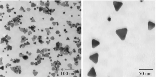
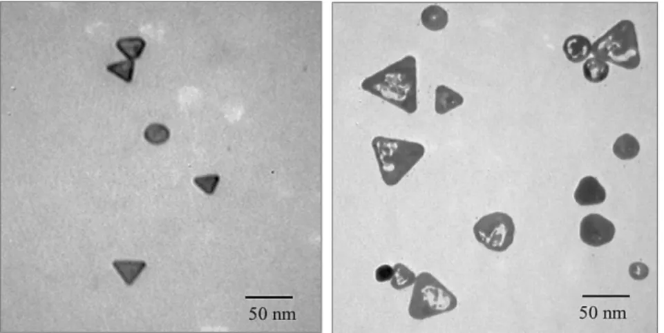
4. Gold hollow nanotriangles……….55
4.1. Synthesis of the sacrificial template – Ag nanoprisms………...56
4.2. Synthesis of Au-framed Ag nanoprisms………...60
5. PdCu@Au core-shell nanotripods………...66
5.1. Synthesis of PdCu nanotripods………67
5.2. Synthesis of PdCu@Au core-shell nanotripods………...70
6. Conclusion………...74
References………...75
Chapter 3 : Directed assembly of gold nanorods………....79
1. Introduction……….81
2. AuNRs covalently linked through a thiol-terminated organic assembler……89
2.1. Synthesis of the organic assembler I………....89
2.2. Synthesis of the organic assembler II………..93
2.3. Phase transfer of AuNRs from water to DCM………95
2.4. AuNRs self-assembly in DCM………96
2.5. AuNRs self-assembly in water………....98
2.6. Optical characterization of AuNRs trimers………....104
3. Self-assembly of AuNRs via hydrophobic interactions………....107
3.1. Synthesis of the organic assembler III………...107
3.2. Synthesis of the organic assembler IV………...108
3.3. Grafting of PS chains onto the tips of the AuNRs……….109
3.4. AuNRs self-assembly via organic assembler III………....110
3.5. AuNRs self-assembly via organic assembler IV………....111
4. Conclusion………...113
References………115
Chapter 4 : Assembly of gold hollow nanotriangles on DNA origami templates….119 1. Introduction………...121
2. Formation of a rectangular DNA origami………..127
3. Modified DNA origami for the assembly of AuHTs and fluorescent dyes...128
3.1. Synthesis of a nanostructure………129
3.2. Optical characterization of a nanostructure……….132
4. Conclusion………..136
References………....137
Conclusions and perspectives……….139
1. Conclusions……….141
2.1. Fabrication of a plasmonic switching device based on a DNA origami
template………..142
2.2. Fabrication of a plasmonic switching device by surface-plasmon-triggered two-photon polymerization……….….145
References………...149
Annexes………...151
Annex 1 : Synthesis of the organic assemblers I-IV………...153
Annex 2 : DNA strands used for the assembly of DNA origami…………....169
Annex 3 : Characterization techniques………173
1
3 MOTIVATION
Nanotechnology, the science of manipulating matter at the near-atomic scale, has an enormous potential for the future development. In the modern society, the ever-increasing demand for smaller, faster and more efficient electronic devices is undeniable. Next generation technologies will thus require miniaturization and integration of existing devices and circuits.
Plasmonics is currently the key technology that enables the revolution in the integrated optical circuits. The intrinsic functionality of plasmonic nanodevices relies on the ability of metallic nanostructures to concentrate and manipulate light in the nanoscale regions. Owing to their unique optical properties, plasmonic nanoparticles offer powerful tools for optical signal processing, sensing and imaging [1].
However, the practical integration of plasmonic architectures into modern nanodevices requires the development of the synthetic techniques that provide the control over their optical features.
The most powerful mean for tailoring the optical properties is the control over plasmonic nanoparticle shape [2]. Additionally, the self-assembly of nanoparticle into the complex hierarchical architectures with a controllable manner provides a promising way to obtain the collective optical properties that exceed those of the individual subunits. In order to fully exploit the self-assembly of nanoparticles in technological applications, a high level of direction and control is required. Thus, the assembly of hybrid nanodevices from different photonic building blocks offers a route to create novel multifunctional nanomaterials for a wide range of applications such as optoelectronics, information transfer and storage, but also in enhancing certain optical processes as surface enhanced Raman scattering or fluorescence [3]–[5].
4 OUTLINE OF THE THESIS
Chapter 1 provides an introduction into the field of plasmonics, starting with the elementary description of surface plasmon polaritons and localized plasmons. A particular focus is put to light guiding and optical addressing via metallic nanostructures. In addition, the scope and the aims of this thesis are presented.
Chapter 2 describes the synthetic routes that have been developed to prepare various noble metal nanostructures that have been employed as building blocks for the plasmonic nanodevice fabrication. In particular, the bottom-up synthesis and characterization of gold nanorods, gold hollow triangles and gold coated tripods are presented.
Chapter 3 is devoted to the fabrication of gold trimers, i.e. three gold nanorods linked by different organic assemblers. Multistep syntheses of new organic molecules and their use as linkers are presented. The optical characterization of the fabricated gold trimers is also discussed.
Chapter 4 describes the fabrication of nanoarchitectures composed of gold hollow triangles and fluorescent dyes assembled via DNA origami. The synthesis and modification of a DNA origami that enables the accurate positioning of gold hollow nanotriangles and fluorophores are shown. Light propagation in the fabricated nanodevice is investigated.
Conclusions and perspectives summarize the main results obtained during this thesis and describe some perspective of this work.
Annexes provide details about the multistep synthesis of the organic linkers, the list of the sequences used to fold a DNA origami, and the description of the equipment used for the structural and optical characterization of the samples.
5 REFERENCES
[1] D. K. Gramotnev and S. I. Bozhevolnyi, “Plasmonics beyond the diffraction limit,”
Nat. Photonics, vol. 4, no. 2, pp. 83–91, 2010.
[2] X. Lu, M. Rycenga, S. E. Skrabalak, B. Wiley, and Y. Xia, “Chemical synthesis of novel plasmonic nanoparticles,” Annu. Rev. Phys. Chem., vol. 60, no. 1, pp. 167–192, 2009.
[3] N. E. Motl, A. F. Smith, C. J. DeSantis, and S. E. Skrabalak, “Engineering plasmonic metal colloids through composition and structural design,” Chem. Soc. Rev., vol. 43, no. 11, pp. 3823–3834, 2014.
[4] C. Hamon and L. M. Liz-Marzán, “Hierarchical Assembly of Plasmonic Nanoparticles,” Chem. - A Eur. J., vol. 21, no. 28, pp. 9956–9963, 2015. [5] O. Benson, “Assembly of hybrid photonic architectures from nanophotonic
7
CHAPTER 1
9
INTRODUCTION
In the age of the information and communication technology, there is a great need for faster information transport and processing capabilities.
Although the progress towards smaller, faster and more efficient electronic devices over the last five decades is undeniable, the scaling of those devices at nanometer level has brought up issues with a delay time for signal propagation and communication between different components. Optical interconnects have been suggested as an alternative because of their huge data carrying capacity, but they are limited in size by the laws of diffraction to about half a wavelength of light. The size mismatch between the two conventional technologies is an obvious obstacle to further advances in many areas of modern science, but can be overcome by the emerging field of plasmonics (Figure 1.1) [1], [2].
Figure 1.1 : Plasmonics breaks the limits in the speed of nanoscale electronics and the size of terahertz dielectric photonics [3].
The term plasmonics comes from the concept of plasmon, which refers to the resonant oscillations of free electrons in metal upon illumination. At the surface of a metal, the resonant interaction of charge oscillation and electromagnetic field of light creates surface plasmons (SPs), which are strongly influenced by boundary conditions. SPs are generated when a photon strikes the surface of a metal. They can be imagined as ripples created in a quiet pond upon tossing a rock. In this case, the ripples are composed of oscillating electrons with nanometer-scale wavelengths. Once in motion, these oscillations, or surface plasmons, can gather more light and carry it over substantial distance [4].
10
If such metallic structures are reduced to the nanometer scale, light can be concentrated and manipulated by objects much smaller than its wavelength [5].
SPs thus provide an opportunity to focus the light to tiny spots, direct and route it along complex circuits below the resolution limit of conventional technologies. As it offers the miniaturization of devices with a capacity of photonics, plasmonics can bridge the gap between existing devices and create high-speed, high-capacity and low-power next generation optical nanodevices.
Even though the first studies describing surface plasmons date back to the 1902, when Wood observed “anomalies” in spectra of optical reflection on metallic gratings [6], the history of plasmon based applications began 50 years after, when Ritchie predicted the existence of self-sustained collective excitations at metal surfaces [7]. In his pioneering work, he studied the impact of the film boundaries on these collective excitations and found the loss phenomena associated with excitation of surface collective oscillations. In the following years, the existence of those collective oscillations was experimentally confirmed by Powell and Swan [8]. Finally, in 1960, Stern and Ferrell extended Ritchie’s theory and linked it with surface plasmons [9]. From this date, scientists have been rediscovering the optical response of nanoparticles in a variety of different contexts, resulting in rapid advances in nanofabrication and subwavelength optical characterization, theoretical approaches and the expansion of plasmonics in broad areas of applications. The plasmonic nanostructures gained a great interest in data storage [10], microscopy [11], sensing [12], optoelectronics [1], optical computing [4], information transfer [13], but also disease diagnosis and therapy [14].
In the following sections, we will first introduce the topic of nanoplasmonics, and the different optical phenomena that make it so attractive for numerous applications. A particular focus will be put on surface plasmon generation, propagation and finally, manipulation and routing.
In the last section, we will describe the aim of our project dedicated to the fabrication of branched plasmonic nanostructures for the active guiding of light.
11
1. NANOPLASMONICS
The most attractive research on SPs relies strongly on their ability to concentrate and channel light in subwavelength structures. The study of such optical phenomena in the nanoscale vicinity of metal surfaces is called nanoplasmonics [15].
When a bulk material is exposed to an external electromagnetic field, the charge inside it is set in motion. Electrons displace with respect to the lattice ions, creating the charges at the opposite surfaces. Due to the attraction forces between the charges, there is also a restoring force, which forms an electron oscillator. When the applied electromagnetic field is at the right frequency, its oscillations can couple to an oscillatory mechanical motion of charges in metal, creating a surface plasmon [16].
Also, SPs can be strongly confined at the surface of metallic nanoparticles. This effect, known as localized surface plasmon (LSP), occurs when the electrons in nanoparticle respond to illumination by absorption and radiation, enhancing the electromagnetic field around the nanoparticle. Both features of surface plasmons will be reviewed in the following sections.
1.1. Surface plasmon polaritons
Propagating surface plasmons, also called surface plasmon polaritons (SPPs), are electromagnetic waves that propagate along the planar interface between a conductive metal and dielectric (a non-conductive medium like air or glass). Propagation arises from their hybrid nature - coupling between surface charges and electromagnetic field in the dielectric medium, which leads to different features of SPPs mode [17]. The basics of surface plasmons are shown in Figure 1.2.
12
Figure 1.2 : (a) Hybrid nature of SPPs – both electromagnetic wave and surface charge character at metal–dielectric interface. (b) The perpendicular field Ez decays
exponentially with a decay length δd in the dielectric and a decay length of δm in the
metal. (c) Momentum mismatch between the surface plasmon mode and a free space photon of the same frequency [17].
SPPs can propagate at the interface as surface bound electromagnetic waves in single, flat interfaces or in dielectric/metal multilayers system. The intensity of those electromagnetic waves is maximal at the interface and decays exponentially into both the metal and the dielectric as the distance from the interface increases. In the dielectric medium, perpendicular to the surface of metal, the decay length into the dielectric (δd) is in range of the half wavelength of the light used, while the decay length into the metal (δm) is limited by the certain depth beyond which the electromagnetic field cannot penetrate in metal, so-called skin depth (Figure 1.2) [17].
Another significant feature of SPPs is that on a planar surface , the wave vector of the SP, kSP, is always higher than the one of the electromagnetic wave of the same frequency propagating in the free space, k0, where k0 = ω/c (Figure 1.2). The increased momentum of the SPP occurs due to the strong interaction between light and surface charges. Due to the larger propagation constant, SPPs on such interfaces cannot be excited directly by light propagating in the dielectric, and they cannot radiate into the dielectric. Thus, SPPs are also called “dark waves”. The momentum mismatch between the SPP mode and incident light can be overcome by modifying the wavevector of the incident light using different optical techniques, such as prism, grating or waveguide coupling to enhance the momentum of incident light or near-field excitation [18].
13
Owing to their unique optical properties, SPPs exhibit a great potential in a variety of applications. Their ability to control light at a scale much lower than its wavelength makes them an interesting tool in near-field optics.
Moreover, generation of SPPs enhances the electromagnetic field in the metal-dielectric interface, resulting in their extreme sensitivity to surface conditions. This sensitivity is a point of interest in the development of different surface plasmon polariton-based devices, because it is responsible for surface-enhanced optical phenomena such as Raman scattering and fluorescence. Such devices are commonly used for chemical and biological sensing, but as well in data storage and solar cells [19].
1.2. Localized surface plasmons
For centuries, humans have been using nanoparticles and their plasmonic effects in the creation of ornamental goblets and other stain glass without knowledge of their microscopic structure.
One of the oldest examples is the Lycurgus Cup, which dates from the fourth century A. D. When the cup is viewed in ambient lighting, the plasmonic scattering gives its green color, but when illuminated from the inside, it appears red (Figure 1.3). This effect occurs due to its transmission and absorption at longer and shorter wavelengths, respectively. Today, it is known that the dichroic nature arises from the gold and silver embedded in the glass and that the light scattering is attributed to localized surface plasmon resonance (LSPR) [20].
Figure 1.3 : The Lycurgus cup in reflected (green) and transmitted (red) light [20].
Unlike the SPPs, which propagate along a flat metal-dielectric interface, localized plasmon modes are stationary oscillations of the surface charge density at the boundaries of a metallic particle smaller than the wavelength of light (Figure 1.4).
14
Figure 1.4 : A scheme of (a) surface plasmon and (b) localized surface plasmon [21]. When the incident light interacts with a metallic nanoparticle, its electric field periodically displaces the electrons inside the nanoparticle with respect to the lattice ions, creating charges at opposite surfaces which then feel repulsive forces. Due to the attraction between electrons and metallic nuclei, conduction electrons at the surface of the metal oscillate coherently in resonance with the incident light frequency. Those collective oscillations of electrons create a LSPR at the surface of the metallic nanoparticle (Figure 1.5) [22], [23].
Figure 1.5 : Collective oscillations of conduction electrons in a spherical metallic nanoparticle demonstrating the displacement of the conduction electron cloud relative to the nuclei [24].
The optical extinction of noble metal nanoparticles has a maximum at the plasmon resonant frequency, which occurs in the visible or near-infrared part of the spectrum. Since the closed geometrical boundaries of nanoparticles sustain localized oscillations of the surface, LSPR response of metal nanostructures depends on their size and shape, but also on the chemical composition and refractive index of the nanoparticles and on the nature of the surrounding
15
environment. Variations of those parameters provide a powerful tool for controlling and manipulating the LSPR response, because even the slightest changes in aspect ratio or corner sharpness can have a large impact on the optical properties of nanoparticles [25].
The ability of LSPR to localize and enhance optical fields around the nanoparticle makes them very attractive in different applications such as surface-enhanced Raman scattering (SERS), fluorescence enhancement, refractive index (RI) measurement, biomolecular interaction detection and plasmon resonance energy transfer (PRET) [26].
1.3. Coupling of surface plasmons
Light-induced charge polarization on the nanoparticle surface leads to resonantly enhanced electromagnetic field inside the nanoparticle. Consequently, the concentration of EM energy strongly enhances the EM field in the immediate vicinity of the nanoparticle. When nanoparticles are in close proximity, their localized modes can thus couple via electromagnetic interactions, resulting in coupled plasmon oscillations.
For metallic particles much smaller than the wavelength of the exciting light, plasmon excitations produce an oscillating dipole field. Thus, each excited particle acts as an electric dipole, and an array of particles can be considered as an array of interacting dipoles. Due to electromagnetic interactions between the localized modes, nanoparticle assemblies induce a change in spectral position, width or amplitude, when compared to the single particle.
Two types of interparticle electromagnetic coupling can be distinguished by the magnitude of the distance between the nanostructures (d): near-field and far-field coupling. If the particles are closely packed in a chain (d << λ), they interact through their near-fields, while an increase of the inter-particle distance (d ≈ λ) induces a transition to far-field coupling. Once the inter-particle distance exceeds ~2.5 times the particle size, the particles behave as isolated [27]–[29]. In small particle arrays, the coupling occurs mainly in the near-field.
The direction of coupling-induced shift of the plasmon resonance is determined by the Coulomb forces associated with the polarization of the incident light. For the longitudinal modes, the inner restoring force in each particle is weakened owing to the attractive forces between two charges of adjacent nanoparticles (Figure 1.6 b). Thus, the plasmon resonance maximum is red-shifted in comparison with the resonance of an individual particle. In
16
contrast, for the excitation of the transverse mode, the charge distributions of adjacent nanoparticles act cooperatively, increasing the restoring force, and causing the blue-shift of the LSP (Figure 1.6 c) [30], [31].
Figure 1.6 : Electromagnetic interaction between closely spaced nanoparticles: (a) an isolated particle, (b) a pair of close particles with the polarization of the exciting field parallel to the long particle pair axis and (c) orthogonal to the long particle pair axis [32].
In addition, the shifts in a resonance energy strongly depend on the geometry of the particle array, its length and the interparticle distance [18].
In a large array of nanoparticles, each particle is exposed to the near-field of a large number of particles and the coupling is stronger, leading to a larger red-shift. Moreover, the red shift can be induced by shortening the distance between the nanoparticles in the assembly, due to the rapid decay of a nanoparticle’s near-field with distance [31].
The interparticle plasmon coupling thus offers an additional tool for tuning the NPs optical response. Great advances have been made in the fabrication of plasmonic assemblies by bottom-up and top-down techniques for different applications, such as surface enhanced Raman scattering (SERS), biosensing and medical applications [30].
2. NANOPLASMONICS FOR LIGHT MANIPULATION
For future development of chip-scale electronics and photonics, it is essential to provide communication channels that allow controlled information and energy transport at the nanometer level. Plasmon waveguides, fabricated from metallic NPs, offer a unique way to
17
concentrate and guide EM waves at the nanoscale, which makes them attractive as building blocks for modern nanodevices [33], [34].
However, the full integration of optical waveguides into all-optical circuits requires additional active control over the plasmonic response. The creation of active plasmonic devices like modulators and switchers, in which plasmonic signal can be specifically addressed as well as switched on and off, presents a next big step towards the complete development of the next-generation chips [35].
Another obstacle that holds back the implementation of plasmon waveguides in compact nanodevices is the propagation loss due to increased mode confinement.
In many cases, the attenuation of the electromagnetic wave due to absorption in the metal limits the energy propagation distance to several micrometers. Consequently, not all of the mentioned waveguides are able to guide the subwavelength plasmonic signal equally.
These energy losses can be compensated through the improvements of near-field coupling, or the use of low-loss substrates [36].
In the following sections, we will describe energy propagation in several plasmonic waveguides. Then, the propagation through sharp corners and the active switching of plasmonic signal will be reviewed. Finally, we will look at the possibilities to compensate the energy loss in such systems.
2.1. Plasmonic waveguides
In the last 20 years, many researches have been focusing their attention to the light guiding and optical addressing via metallic nanostructures.
Various types of plasmon waveguides have been fabricated, mainly by top-down nanolithography techniques. Chains of nanoparticles, thin metal films, metal slits, grooves, nanowires and sharp metal wedges have been proposed to guide the electromagnetic energy for potential plasmonic nanodevices [37].
Although the use of such metal nanostructures as waveguides was described in different theoretical studies [38], [39] and numerical simulations [40], [41], experimental proofs remained rare.
18
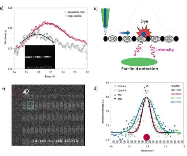
Maier and co-workers [42] were the first ones to confirm the subwavelength-sized light guiding via near-field coupling between adjacent plasmonic nanoparticles over around a 0.5µm distance. By electron-beam lithography, they fabricated plasmonic waveguides consisting of silver nanorods with dimensions of 90 nm × 30 nm and a constant space of 50 nm between adjacent rods (Figure 1.7 a). The plasmon waveguides arranged in a grid are shown in Figure 1.7 c. The long axis of the individual nanorod was oriented perpendicular to the waveguide chains axis to allow an increased near-field coupling.
The scheme of the experiment is shown in Figure 1.7 b. The tip of a scanning near-field optical microscope (SNOM) was used as an illumination source for local excitation of the nanoparticle plasmon waveguide. Upon the excitation of one rod, the localized plasmon modes of rods in an array coupled via electromagnetic interactions, resulting in energy propagation.
Such electromagnetic energy transport through an array of particles was probed by randomly dispersing fluorescent nanospheres, which show strong absorption near the excitation wavelength, on the grid containing the waveguides. The excitation propagation along the array of nanostructures excited the fluorescent probes, whose fluorescence intensity was then collected in the far-field. The energy transport was visualized via the increase of the spatial width of the fluorescent probe close to a plasmon waveguide, compared to the width of an isolated probe (Figure 1.7 d) [43].
19
Figure 1.7 : Light guiding via near-field coupling between adjacent plasmonic NPs: (a) Plasmon resonance of silver rods and a chain of closely spaced rods upon the transverse illumination with an inset showing a SEM image of a waveguide; (b) scheme of the experiment showing the local excitation and detection of the EM energy transport in a plasmonic NPs array; (c) SEM image of the waveguides arranged in a grid where red box shows the control area outside the grid, with free fluorescent probes only, and the green box shows an area where probes are in close proximity to the waveguides; (d) compared intensities of the fluorescent signals for the control probes and for the probes close to the plasmonic waveguides [42].
Bozhevolnyi et al. [44] demonstrated the guiding of the SPPs along the grooves of a triangular shape milled into a gold surface. They experimentally confirmed the guiding of a plasmonic signal through 0.6 µm wide and 1 µm deep nanogrooves with the propagation length on the order of 100 µm. Examples of SPP propagation for functional structures such as waveguide splitters and interferometers is shown in Figure 1.8.
20
Figure 1.8 : (a, d) SEM images; (b,e) topographical and (c,f) near-field images of SPP groove waveguides milled into a metal film. Inset shows depth and angle of the groove [18].
Few examples of plasmonic waveguides synthetized by bottom-up synthetic approach (i.e. colloidal chemistry) include metal nanowires. For example, Ditlbacher et al. [45] showed the SPs propagation along silver nanowires. When they focused a laser beam onto one end face (polarization oriented along the nanowire axis) of a 18.6 μm long nanowire, a part of the incident laser intensity was scattered into a surface plasmon mode, propagating towards the distal end of the wire. A part of the plasmon intensity was there scattered to light, which was then detected with a conventional optical microscope (Figure 1.9). The chemical synthesis of those nanostructures provided a better control over crystal and surface structure compared to the lithography fabrication, leading to minimized energy losses due to the metal absorption and thus a longer propagation length (~10µm).
21
Figure 1.9 : Silver nanowire as a plasmonic waveguide: (a) optical excitation scheme, where I is input and D is distal end of the wire; (b) microscopic image of the nanowire - the bright spot is focused exciting light, while the arrow points to light scattered from the distal wire end; (c) near-field image of an area in the white box in (b); (d) cross-cut along the chain shown in (c) [45].
2.2. Routing the light at the nanoscale
Scaling down existing optical devices to ultimate limits for the fabrication of new, highly integrated photonic circuits strongly relies on nanoarchitectures able to manipulate the light at the nanoscale. However, more complex, functional elements such as controllable plasmon routers, multiplexers and switchers, are necessary for the development of modern information technologies. The key to the development of nanodevices is the fabrication of active components able to specifically address and route the plasmonic signal, as well switch it between on and off position.
Owing to their ability to simultaneously support different wavelengths of light and manipulate them independently, plasmon waveguides are good candidates for active switchers or routers in plasmonic circuits [46], [47]. However, a deep understanding of the ability of waveguides to bend the direction of a traveling wave at corners and intersections is necessary for the design of modern plasmonic switches.
Maier et al. [22] showed the design of an all-optical switch based on the EM energy guiding through corners and tee structures via the near-field coupling of adjacent NPs. By calculating
22
the power transmission coefficients (ƞ) for energy transport around such elements, they showed that coefficients close to 100 % are possible for propagation around 90° corners for certain polarizations, and that lossless signal splitting can occur in tee structures (Figure 1.10). Those coefficients depend on the geometry of the structure, the frequency, and the polarization directions of the plasmon waves which enter and exit a structure [22], [39].
Figure 1.10 : Calculated power transmission coefficient in nanoparticle chain for a 90° corner (left) and a tee structure (right) for the longitudinal (L) and transverse mode (T). The ƞ value of 1 corresponds to 100 % transmission [22].
Maier’s study confirmed the ability of plasmon waveguides to transport EM energy around 90° corners and split via tee structures. However, the energy cannot propagate selectively in only one branch of the multi-branched structures. Due to the plasmon coupling effect, the energy propagates equally in the two branches of the nanoarchitectures, which then works only as a passive light guiding system.
Hence, the addressable routing of light and its switching between different elements needs to be developed to create controllable plasmonic structures with active functionality.
One possible way to selectively route the plasmonic signal into a branched metallic nanostructure is to control the polarization of the incoming light, as shown by Fang et al [46]. The branched nanowire system studied by the authors for directional guiding is shown in Figure 1.11.
23
Figure 1.11 : Optical image of branched silver nanowire structure excited by a laser. The inset shows a SEM image of the branch intersection, where the scale bar is 200 nm. The gap between the two wires is 10 nm [46].
Upon illumination of end 1 of the wire, launched SPPs propagate and the light can be controlled to emit from end 2 or 3 through varying the illuminating polarization. For specific polarizations, emission of the main wire can be at the minimum, while the one of the side wire is at maximum, and vice versa.
Moreover, branched nanowires can selectively route SPPs launched with different free-space wavelengths towards different ends of the structure, as shown in Figure 1.12. When two lasers with different wavelengths, 633 and 785 nm, were focused at the end 1 of the structure, the rotation of the polarizer caused a 633 nm laser coming out mainly from the end 2 and a 785 nm laser coming out from the end 3. Such routers, which can work simultaneously for multiple wavelengths, fulfill the requirements given for the full development of future nanophotonic devices, circuits, and networks.
24
Figure 1.12 : (a) Emission power at the ends of the main and the branch wire as a function of the incident polarization angle θ. Emission of the branched wire is maximal when θ=27° and minimal when θ=117°; (b,c) local electric filed distributions at the maximum (b) and minimum (c) emission of a branch wire; (d) routing for multiple wavelengths - emission intensity from ends 2 and 3 as a function of the polarization angle for 633 and 785 nm wavelength excitation and the corresponding spectra for the wires 2 (up) and 3 (down) [46].
Tuning the dielectric function of the surrounding medium is another approach to control the plasmonic response of nanostructures. Such active surrounding medium can be obtained by employing liquid crystals (LCs), stimuli-responsive polymers or photochromic molecules. For example, Hsiao et al. [48] described an all-optical switch composed of Au nanodisk arrays embedded in a photoresponsive LC (Figure 1.13). To induce the switching effect, they used azobenzene derivative as guest material in a LC matrix. Azobenzene molecules were used because they undergo a reversible photochemical reaction between two configurations,
trans- and cis, inducing the realignment of LCs and thus changing the refractive index of the
25
Figure 1.13 : a) Phase transition process in photoresponsive LCs; b) extinction spectra of a photoresponsive LC/Au nanodisk array before (solid curve) and after illumination at normal incidence (dashed curve) [48].
D. Neuhauser and co-workers [49]–[52] have investigated the guiding of plasmonic current via single molecules. Their studies led to the emergence of a new field, named nanopolaritonics. It refers to the ability of dipolar matter such as dye molecules to control the propagation of surface plasmon-polariton waves along metal nanostructures. In such energy transfer, the plasmon firstly affects the molecule by inducing electronic oscillations, and the molecule in turn affects the plasmon propagation through near-field interactions.
In their pioneering work, Neuhauser and Lopata [49] showed that a molecule that has an excitation energy similar to the plasmon resonance frequency of the metal can direct the motion of an electromagnetic radiation. Their system was composed of metal dots in a forklike arrangement, coupled to a two level system with a large transition-dipole moment. By varying the strength and orientation of the molecule, as well as its position with respect to the dots array, they controlled the path of the polariton flow in the forklike junction (Figure 1.14).
26
Figure 1.14 : A switching forklike junction, which is based on the coupling with a dipolar molecule (represented by the arrow) to guide a polarized polariton into one of two possible output paths (here the top one). Transmission spectra through the top and bottom branches are shown in blue and red, respectively. The transmission spectrum for the device without the molecule is shown in black. In this case, the output signals in both branches are identical [49].
More recently, Neuhauser [53] simulated the selectivity of plasmonic motion along a continuous Y-shape gold structure in the presence of a large number of molecules. He considered two cases – first where the space outside the Y-shape structure was filled with aligned molecules, and second where the gold structure was coated with a thin layer of molecules. For both cases, he observed that even at low molecular densities, the energy transport is significantly affected. At low molecular densities, an overall reduction in plasmonic transfer was observed, while the higher densities induced the selectivity due to the hybridization of the molecular and plasmonic field (Figure 1.15).
The field of nanopolaritonics, which enables the control over light transport by changing the direction of the guiding molecular dipoles through an external stimulus, represents a step forward toward light manipulation at the nanoscale. However, the controllable and addressable routing and multiplexing of light remains a big challenge and thus offers an attractive subject for further investigations.
27
Figure 1.15 : a) Schematic illustration of the Y-shape gold structure. The red circle indicates the spot where an external electric field pulse is applied. The boxed regions show where the currents are measured. b) Energies in the two arms (up and down) and in the back arm as a function of frequency for a Y-shape gold structure in a space filled with aligned dipole molecules. For a high molecular density, a strong selectivity arises from the plasmon-dipole interaction [53].
2.3. Energy loss and power compensation
The attenuation of the SPPs propagating through a plasmonic waveguide due to the absorption in the metal limits their integration to compact optical circuits.
There is a trade-off between the confinement and loss - the more strongly the optical mode is confined to the metallic interface, the greater is the overlap with the metal, resulting in energy dissipation [54]. For example, nanoparticle arrays and nanowire waveguides can significantly enhance the confinement, but with large attenuation losses, which limits the light propagation length to few micrometers or less. On the other side, low loss over a propagation length of a few millimeters is possible in waveguides such as thin metal films embedded in homogeneous dielectric background, but the associated fields are weakly confined in the perpendicular direction [18].
Although some loss compensation can be realized through the optimization of the nanostructure synthesis with improvements of the geometry, material and structural imperfections, optical loss is also determined by the physical properties of the metal. Thus, further studies dedicated to the development of novel loss compensation methods are required.
28
Recently, hybrid plasmonic waveguides that consist of a metallic region separated from a dielectric zone with a high refractive index by a low index nano-slot, have been proposed to compensate the propagation losses. The low-index gap between the metal and the dielectric facilitates the hybridization of dielectric and plasmonic modes, allowing the efficient nanoscale light transport with reasonable propagation distances [36], [55], [56].
Another approach to simultaneously increase the localization of the field and the propagation length is the introduction of an optical gain medium in the structure. It was confirmed both theoretically and experimentally that metal nanostructures embedded into a medium with optical gain, such as dye molecules, quantum dots or fluorescent polymers can overcome confinement-loss trade-off [57].
3. AIM OF THE PROJECT
The work-package ‘Nanopolaritonics’ of the InPhotArch (Integrated Photonics Architectures) LAPHIA project constitutes the frame of this thesis.
The overall objective of the project is to investigate the complex EM energy transfer in branched gold nanostructures by promoting the path selectivity via plasmon-dipole interaction.
Even though light routing in Y-shape gold nanostructure (engineered by top-down approaches) in the presence of molecules have been extensively studied theoretically by D. Neuhauser, nanoarchitectures comprising molecules and metallic nanoparticles produced by colloidal synthesis have not been investigated either theoretically or experimentally. Thus, predictions about path selectivity of light in Y-shaped nanostructures have been performed to guide the synthesis of the building blocks required for the nanodevice fabrication.
3.1. Computational simulations
In order to predict the path selectivity of light in the Y-shape gold nanodevice, computational simulations of the propagation of an electromagnetic pulse through a Y-shape gold structure overfilled with anisotropic material were performed. The predictions have been realized by Atsushi Yamada, a postdoc engaged for this purpose in the LAPHIA project.
29
Finite-Difference Time-Domain (FDTD) method was used for calculating the propagation of the electromagnetic field through the material. The time evolution of the electromagnetic field was described by solving Maxwell equations on a grid. Materials were treated classically and represented by a dielectric tensor (for the anisotropic molecular medium) and a Drude-Lorentz model (for gold). This method was applied to the system shown in Figure 1.16 a. The system was composed of three gold nanorods combined in a Y-shape structure, surrounded by an anisotropic molecular medium with molecular polarization direction oriented toward the right-top gold rod, employed to create a change in the direction of a propagating light pulse. The length and the diameter of the gold rod were 20 nm and 10 nm, respectively. Each rod was separated by 5 nm from the center of the Y-shape and oriented with an angle of 120° one from the other (Figure 1.16 b).
Figure 1.16 : a) Schematic illustration of the Y-shape structure system. The positions of the incident light source (purple), the anisotropic layer (blue region and arrows) and the two detectors (red and green dotted line box regions) are illustrated. b) The size of the Y-shape structure system in the xy-plane.
The molecular medium was a material aligned (molecular polarization) with an angle of 35° degree (result of an optimization process) with respect to the x-direction in the xy plane. This molecular part was described by dielectric tensor ε so that:
30 1 | | 0 0 ( ) 1 1 1 ) ( 1 1 1 U U ε Equation 1.1
ε0, ε||, and ε⊥ are the dielectric constant in vacuum and along parallel and perpendicular
directions of molecules, respectively. U(θ) represents a rotation matrix allowing for the tuning of the angle θ (tuning of molecular orientation). The second term of the right-hand side of Eq. 1 thus fixes the polarizations along the parallel and perpendicular directions of the molecules in the xy plane. In this study, no polarization in the perpendicular direction was assumed for simplicity, i.e. ε⊥=1.
In the FDTD simulation, the model in Figure 16 was structured with a grid size of 1.25 nm, where absorbing boundary conditions (ABCs) were set in all directions. The time step was determined by a courant factor of 0.5. The incident light source is represented by a Gaussian point source in space, placed at around 2.5 nm from the edge of the left gold rod. The d-pulse (in time) is thus broadband (white) and polarized along the x-direction (that is, x-component of the electric field). The electric field spectra were measured at the two regions on the right sides of the top and bottom rods as shown by the red and green areas in Figure 1.16.
The electric field spectra measured at the two detected regions at the top and right-bottom with various values of the parameter ε|| of the molecular medium are shown in the
Figure 1.17. The figures clearly show that the right-top region detects stronger electric field than the right-bottom region, indicating path selectivity induced by the aligned molecular medium. The ratio of the two detected spectra (at the peak wavelength) increases from 2 to 5 while increasing the parameter ε|| within the presented range. Furthermore, the path-selectivity
is accompanied by a small shift in frequency, with the signal in the top-right detector always red-shifted with respect to the one in the green channel. Note that the adjustment of the spectra and spectral peaks in this part of the visible region was achieved by an optimization of the size of the gold rods, their inter-distance and their relative configuration. In addition, the path selectivity was optimized by tuning the angle θ, reaching an optimal value of 35°.
31
Figure 1.17 : Electric field spectra detected at the right-top (red) and right-bottom (green) regions of the Y-shape structure with the parallel component of various dielectric constants of the anisotropic medium: (a) ε||=2, (b)ε||=3, (c )ε||=5, (d )ε||=10.
The path-selectivity and the signals in the two branches of a Y-shaped nanostructure can be increased by orders of magnitude by introducing a gain medium in the system, compensating the Ohmic losses in the metal particles. Such results, based on a Y-shape structure of gold cubes, were shown by Yamada et al. [58], where a very realistic model has been used to represent both the gain and anisotropic media. Path selectivity, with a ratio of around 100, has been found in this study, with the concomitant apparition of path-selective lasing. Moreover, very similar results can be obtained while using gold open triangles or even fully joined tripod structures (all structures with three branches).
3.2. Scope of the thesis
In the framework of the InPhotArch project, this thesis was dedicated to the fabrication of multibranched gold nanostructures and to investigate the EM energy transfer in them. Three types of structures have been designed. The first one is similar to the one described in Figure
32
1.16 and is composed of three gold nanorods linked together via a tripodal organic molecule or precisely positioned from each other via a DNA origami template. The two others are hollow gold nanotriangles and gold-coated nanotripods.
Upon the local excitation of one branch of such multi-branched structures, plasmons propagate equally into the two other branches. The plasmon propagation can be visualized by placing close to the tips of these branches two different emitters that both efficiently adsorb at the wavelength of the propagating waves. Due to the local EM field enhancement induced by the propagating SPS, the emitters should emit light of similar intensity (Figure 1.18).
Figure 1.18 : a) An illustration of a branched Y-shaped nanostructure composed of three gold nanorods assembled via a rigid organic linker; b) General scheme of light propagation inside the branched metallic nanostructure: Upon the excitation of one nanorod, the plasmonic signal propagates equally in the two other nanorods due to the plasmon coupling effect. The emitters localized near the tips of the nanorods emit light of similar intensity.
As stated previously, immersing such Y-shape nanostructure in an anisotropic medium can favor the selective EM energy propagation towards one of the two possible pathways. Figure 1.19 (a) illustrates the plasmon transfer in Y-shaped structure in a medium where dipolar molecules are oriented parallel to its upper branch. The plasmonic signal, generated by the local excitation of one nanorod in a trimer structure, propagates mainly towards the upper branch of the structure. The enhanced EM field at the end of the upper rod consequently enhances the light emission of the emitter positioned at its proximity, demonstrating the selective routing of light. The reverse case is illustrated in Figure 1.19 (b), where the
33
plasmon-dipole interactions guide the light towards the lower branch of the structure, increasing the emission of the emitter localized close to its tip.
Figure 1.19 : Schemetic illustration of a plasmonic switching device where the plasmonic light transport is controlled by inducing a change in the direction of the guiding molecular dipoles through the application of an external stimulus. The grey arrows represent the dipoles with different orientations.
34
4. CONCLUSION
Owing to its capability to confine light to the surface of metallic nanostructures, plasmonics has unique prospects for the design of highly integrated photonic signal-processing systems, nanoresolution optical imaging techniques and sensors. For future developments in nanotechnology, it is essential to provide communication channels that allow controlled information and energy transport at the nanometer level.
By performing FDTD simulations, we showed that the combined design of a Y-shape plasmonic nanostructure and an anisotropic molecular medium could work as a path-selective device, very useful for the future of nanophotonic integrated circuits.
In the following chapters, we will describe the fabrication of plasmonic switching devices based on various Y-shaped plasmonic nanostructures and investigate their ability to route the light at the nanoscale.
35
REFERENCES
[1] R. Zia, J. A. Schuller, A. Chandran, and M. L. Brongersma, “Plasmonics: the next chip-scale technology,” Mater. Today, vol. 9, no. 7, pp. 20–27, 2006.
[2] E. L. Hu, M. Brongersma, and A. Baca, “Applications: Nanophotonics and plasmonics,” pp. 318–340, 2008.
[3] M. L. Brongersma and V. M. Shalaev, “The case for plasmonics,” Science (80-. )., vol. 328, no. 5977, pp. 440–441, 2010.
[4] J. Heber, “Plasmonics: Surfing the wave,” Nature, vol. 461, no. 7265, pp. 720–722, 2009.
[5] L. M. Liz-Marzán, C. J. Murphy, and J. Wang, “Nanoplasmonics,” Chem. Soc. Rev., vol. 43, no. 11, pp. 3820–3822, 2014.
[6] R. W. Wood, “On a remarkable case of uneven distribution of light in a diffraction grating spectrum,” Proc. Phys. Soc. London, vol. 18, no. 1, pp. 269–275, 1902. [7] R. H. Ritchie, “Plasma losses by fast electrons in thin films,” Phys. Rev., vol. 106, no.
5, pp. 874–881, 1957.
[8] C. J. Powell and J. B. Swan, “Origin of the characteristic electron energy losses in aluminum,” Phys. Rev., vol. 115, no. 4, pp. 869–875, 1959.
[9] E. A. Stern and R. A. Ferrell, “Surface plasma oscillations of a degenerate electron gas,” Phys. Rev., vol. 120, no. 1, pp. 130–136, 1960.
[10] H. Ditlbacher, J. R. Krenn, B. Lamprecht, A. Leitner, and F. R. Aussenegg, “Spectrally coded optical data storage by metal nanoparticles,” Opt. Lett., vol. 25, no. 8, pp. 563– 565, 2000.
[11] M. Specht, J. D. Pedarnig, W. M. Heckl, and T. W. Hänsch, “Scanning plasmon near-field microscope,” Phys. Rev. Lett., vol. 68, no. 4, pp. 476–479, 1992.
[12] A. Brolo, “Plasmonics for future biosensors,” Nat. Photonics, vol. 6, pp. 709–713, 2012.
36
effect to design an electrically controlled optical switch,” ACS Nano, vol. 8, no. 10, pp. 10437–10447, 2014.
[14] C. M. Cobley, J. Chen, E. C. Cho, L. V Wang, and Y. Xia, “Gold nanostructures: a class of multifunctional materials for biomedical applications,” Chem. Soc. Rev. Chem.
Soc. Rev, vol. 40, no. 40, pp. 44–56, 2011.
[15] M. I. Stockman, “Nanoplasmonics : The physics behind the applications,” Phys. Today, vol. 64, pp. 39–44, 2011.
[16] E. A. Coronado, E. R. Encina, and F. D. Stefani, “Optical properties of metallic
nanoparticles: manipulating light, heat and forces at the nanoscale,” Nanoscale, vol. 3, no. 10, pp. 4042–4059, 2011.
[17] W. L. Barnes, A. Dereux, and T. W. Ebbesen, “Surface plamons subwavelength optics,” Nature, vol. 424, pp. 824–830, 2003.
[18] S. Maier, Plasmonics: Fundamentals and applications. Springer, 2007.
[19] A. V. Zayats, I. I. Smolyaninov, and A. A. Maradudin, “Nano-optics of surface plasmon polaritons,” Phys. Rep., vol. 408, no. 3–4, pp. 131–314, 2005.
[20] I. Freestone, N. Meeks, M. Sax, and C. Higgitt, “The Lycurgus Cup - A Roman nanotechnology,” Gold Bull., vol. 40, no. 4, pp. 270–277, 2007.
[21] K. M. Mayer and J. H. Hafner, “Localized surface plasmon resonance sensors,” Chem.
Rev., vol. 111, no. 6, pp. 3828–3857, 2011.
[22] S. Maier, M. Brongersma, and P. Kik, “Plasmonics - A route to nanoscale optical devices,” Adv. Mater, no. 19, pp. 1501–1505, 2001.
[23] S. Enoch and N. Bonod, Plasmonics - From basics to advanced topics. Springer, 2012. [24] K. E. Fong and L.-Y. L. Yung, “Localized surface plasmon resonance: a unique
property of plasmonic nanoparticles for nucleic acid detection.,” Nanoscale, vol. 5, no. 24, pp. 12043–12071, 2013.
[25] K. L. Kelly, E. A. Coronado, L. L. Zhao, and G. C. Schatz, “The Optical Properties of Metal Nanoparticles: The Influence of Size, Shape, and Dielectric Environment,” J.
37
[26] Y. Chen and H. Ming, “Review of surface plasmon resonance and localized surface plasmon resonance sensor,” Photonic Sensors, vol. 2, no. 1, pp. 37–49, 2012.
[27] A. O. Pinchuk and G. C. Schatz, “Nanoparticle optical properties: Far- and near-field electrodynamic coupling in a chain of silver spherical nanoparticles,” Mater. Sci. Eng.
B Solid-State Mater. Adv. Technol., vol. 149, no. 3, pp. 251–258, 2008.
[28] S. Maier, M. Brongersma, P. Kik, and H. Atwater, “Observation of near-field coupling in metal nanoparticle chains using far-field polarization spectroscopy,” Phys. Rev. B, vol. 65, no. 19, pp. 1–4, 2002.
[29] I. Tokarev and S. Minko, “Tunable plasmonic nanostructures from noble metal nanoparticles and stimuli-responsive polymers,” Soft Matter, vol. 8, no. 22, pp. 5980– 5987, 2012.
[30] X. Wang, P. Gogol, E. Cambril, and B. Palpant, “Near- and far-field effects on the plasmon coupling in gold nanoparticle arrays,” J. Phys. Chem. C, vol. 116, pp. 24741– 24747, 2012.
[31] P. K. Jain and M. A. El-Sayed, “Plasmonic coupling in noble metal nanostructures,”
Chem. Phys. Lett., vol. 487, no. 4–6, pp. 153–164, 2010.
[32] W. Rechberger, A. Hohenau, A. Leitner, J. R. Krenn, B. Lamprecht, and F. R.
Aussenegg, “Optical properties of two interacting gold nanoparticles,” Opt. Commun., vol. 220, no. 1–3, pp. 137–141, 2003.
[33] G. Lévêque and R. Quidant, “Channeling light along a chain of near-field coupled gold nanoparticles near a metallic film.,” Opt. Express, vol. 16, no. 26, pp. 22029–22038, 2008.
[34] J. R. Krenn, B. Lamprecht, H. Ditlbacher, G. Schider, M. Salerno, A. Leitner, and F. R. Aussenegg, “Non–diffraction-limited light transport by gold nanowires,” Europhys.
Lett., vol. 60, no. 5, pp. 663–669, 2002.
[35] Y. Sun, L. Jiang, L. Zhong, Y. Jiang, and X. Chen, “Towards active plasmonic response devices,” Nano Res., vol. 8, no. 2, pp. 406–417, 2015.
[36] D. Dai and S. He, “Low-loss hybrid plasmonic waveguide with double low-index nano-slots.,” Opt. Express, vol. 18, no. 17, pp. 17958–17966, 2010.
38
[37] D. K. Gramotnev and S. I. Bozhevolnyi, “Plasmonics beyond the diffraction limit,”
Nat. Photonics, vol. 4, no. 2, pp. 83–91, 2010.
[38] J. Takahara, S. Yamagishi, H. Taki, A. Morimoto, and T. Kobayashi, “Guiding of a one-dimensional optical beam with nanometer diameter,” Opt. Lett., vol. 22, no. 7, pp. 475–477, 1997.
[39] M. L. Brongersma, J. W. Hartman, and H. Atwater, “Electromagnetic energy transfer and switching in nanoparticle chain arrays below the diffraction limit,” Phys. Rev. B, vol. 62, no. 24, pp. 356–359, 2000.
[40] M. Quinten, A. Leitner, J. R. Krenn, and F. R. Aussenegg, “Electromagnetic energy transport via linear chains of silver nanoparticles,” Opt. Lett., vol. 23, no. 17, pp. 1331– 1333, 1998.
[41] C. Girard and R. Quidant, “Near-field optical transmittance of metal particle chain waveguides,” Opt. Express, vol. 12, no. 25, pp. 6141–6146, 2004.
[42] S. A. Maier, P. G. Kik, H. A. Atwater, S. Meltzer, E. Harel, B. E. Koel, and A. A. G. Requicha, “Local detection of electromagnetic energy transport below the diffraction limit in metal nanoparticle plasmon waveguides,” Nat. Mater., vol. 2, no. 4, pp. 229– 232, 2003.
[43] L. De Sio, G. Klein, S. Serak, N. Tabiryan, A. Cunningham, C. M. Tone, F. Ciuchi, T. Bürgi, C. Umeton, and T. Bunning, “All-optical control of localized plasmonic
resonance realized by photoalignment of liquid crystals,” J. Mater. Chem. C, vol. 1, no. 45, pp. 7483–7487, 2013.
[44] S. I. Bozhevolnyi, V. S. Volkov, E. Devaux, J.-Y. Laluet, and T. W. Ebbesen, “Channel plasmon subwavelength waveguide components including interferometers and ring resonators,” Nature, vol. 440, pp. 508–511, 2006.
[45] H. Ditlbacher, A. Hohenau, D. Wagner, U. Kreibig, M. Rogers, F. Hofer, F. R. Aussenegg, and J. R. Krenn, “Silver nanowires as surface plasmon resonators,” Phys.
Rev. Lett., vol. 95, no. 25, pp. 1–4, 2005.
[46] Y. Fang, Z. Li, Y. Huang, S. Zhang, P. Nordlander, N. J. Halas, and H. Xu, “Branched silver nanowires as controllable plasmon routers,” Nano Lett., vol. 10, no. 5, pp. 1950–
![Figure 1.1 : Plasmonics breaks the limits in the speed of nanoscale electronics and the size of terahertz dielectric photonics [3]](https://thumb-eu.123doks.com/thumbv2/123doknet/14592605.730206/26.892.268.620.516.786/figure-plasmonics-breaks-nanoscale-electronics-terahertz-dielectric-photonics.webp)
![Figure 1.13 : a) Phase transition process in photoresponsive LCs; b) extinction spectra of a photoresponsive LC/Au nanodisk array before (solid curve) and after illumination at normal incidence (dashed curve) [48]](https://thumb-eu.123doks.com/thumbv2/123doknet/14592605.730206/42.892.189.714.103.441/figure-transition-photoresponsive-extinction-photoresponsive-nanodisk-illumination-incidence.webp)

![Figure 2.6 : Mechanism of nanorod growth from CTAB-capped gold seeds in the presence of silver ions [29]](https://thumb-eu.123doks.com/thumbv2/123doknet/14592605.730206/69.892.194.702.239.673/figure-mechanism-nanorod-growth-ctab-capped-presence-silver.webp)