HAL Id: tel-01870022
https://tel.archives-ouvertes.fr/tel-01870022
Submitted on 7 Sep 2018
HAL is a multi-disciplinary open access
archive for the deposit and dissemination of sci-entific research documents, whether they are
pub-L’archive ouverte pluridisciplinaire HAL, est destinée au dépôt et à la diffusion de documents scientifiques de niveau recherche, publiés ou non,
High-performance coarse operators for FPGA-based
computing
Matei Valentin Istoan
To cite this version:
Matei Valentin Istoan. High-performance coarse operators for FPGA-based computing. Computer Arithmetic. Université de Lyon, 2017. English. �NNT : 2017LYSEI030�. �tel-01870022�
N°d’ordre NNT : 2017LYSEI030
THESE de DOCTORAT DE L’UNIVERSITE DE LYON
opérée au sein de
(INSA de Lyon, CITI lab)
Ecole Doctorale : InfoMaths EDA 512
(Informatique Mathématique)
Spécialité/ discipline de doctorat
: InformatiqueSoutenue publiquement le 06/04/2017, par :
Matei Valentin Iştoan
High-Performance Coarse Operators
for FPGA-based Computing
Devant le jury composé de :
IENNE, Paolo Professeur des Universités, EPFL, Lausanne Rapporteur CHOTIN-AVOT, Roselyne Maître de Conférences HDR, UPMC Rapporteur THOMAS, David Senior Lecturer Imperial College London, London Examinateur PETROT, Frédéric Professeur des Universités, ENSIMAG, Saint-Martin d’Heres Président SENTIEYS, Olivier Professeur des Universités, ENSSAT, Lannion Examinateur DE DINECHIN, Florent Professeur des Universités INSA-Lyon Directeur de thèse
©2017 – Matei Iştoan all rights reserved.
Thesis advisor: Professor Florent Dupont de Dinechin Matei Iştoan
High-performance Coarse Operators for FPGA-based
Computing
Abstract
Field-Programmable Gate Arrays (FPGAs) have been shown to sometimes outperform main-stream microprocessors. The circuit paradigm enables efficient application-specific parallel computa-tions. FPGAs also enable arithmetic efficiency: a bit is only computed if it is useful to the final result. To achieve this, FPGA arithmetic shouldn’t be limited to basic arithmetic operations offered by mi-croprocessors.
This thesis studies the implementation of coarser operations on FPGAs, in three main directions: New FPGA-specific approaches for evaluating the sine, cosine and the arctangent have been de-veloped. Each function is tuned for its context and is as versatile and flexible as possible. Arithmetic efficiency requires error analysis and parameter tuning, and a fine understanding of the algorithms used.
Digital filters are an important family of coarse operators resembling elementary functions: they can be specified at a high level as a transfer function with constraints on the signal/noise ratio, and then be implemented as an arithmetic datapath based on additions and multiplications. The main result is a method which transforms a high-level specification into a filter in an automated way. The first step is building an efficient method for computing sums of products by constants. Based on this, FIR and IIR filter generators are constructed.
For arithmetic operators to achieve maximum performance, context-specific pipelining is required. Even if the designer’s knowledge is of great help when building and pipelining an arithmetic data-path, this remains complex and error-prone. A user-directed, automated method for pipelining has been developed.
This thesis provides a generator of high-quality, ready-made operators for coarse computing cores, which brings FPGA-based computing a step closer to mainstream adoption. The cores are part of an open-ended generator, where functions are described as high-level objects such as mathematical expressions.
Contents
1 Introduction 1
1.1 Context: Computer Arithmetic for Reconfigurable Circuits . . . 1
1.2 Objectives . . . 2
1.3 Outline of the Thesis . . . 3
2 Arithmetic on FPGAs 5 2.1 FPGAs: Reconfigurable Programmable Devices . . . 5
2.1.1 Logic elements . . . 7
2.1.2 Multiplier blocks . . . 11
2.1.3 Memory blocks . . . 13
2.2 Arithmetic for FPGAs . . . 14
2.2.1 Fixed-point Formats . . . 14
2.2.2 Sign-extensions . . . 14
2.2.3 Rounding Errors, and Accuracy . . . 15
2.3 The FloPoCo Project . . . 15
2.3.1 Computing Just Right – Last-bit Accuracy . . . 16
2.3.2 Overview of the Project . . . 16
2.3.3 Operators . . . 18
2.3.4 Targets . . . 20
I
Automatic Pipeline Generation for Arithmetic Operators
23
3 Operators and Pipelines 27 3.1 Lexicographic Time . . . 273.2 Pipelining in FloPoCo 4.0 . . . 28
3.3 State-of-the-Art on Automatic Pipelining . . . 35
4 Automatic Pipelining in FloPoCo 5.0 41 4.1 The Signal Graph . . . 44
4.2 The Scheduling Problem . . . 47
4.3 On-line Scheduling of the S-Graph . . . 47
4.4 VHDL Code Generation . . . 51
4.5 New Targets . . . 53
4.6 Results . . . 55
5 Resource Estimation 61
5.1 Related Work . . . 61
5.2 User-guided Resource Estimation . . . 63
5.3 User-guided Resource Estimation for the New Design Paradigm . . . 64
II
Bitheaps and Their Applications
67
6 Bitheaps 69 6.1 Technical Bits . . . 75 6.1.1 Bitheap Structure . . . 75 6.1.2 Signed Numbers . . . 81 6.1.3 Bits . . . 82 6.1.4 Compressors . . . 82 6.2 Bitheap Compression . . . 866.3 Results on logic-based integer multipliers . . . 91
6.4 Concluding Remarks on Bitheaps, Compressors and Compression Strategies . . . . 96
7 Multiplication 99 7.1 FPGAs and Their Support for Multiplications . . . 99
7.2 Multipliers, Tiles and Bitheaps . . . 100
7.3 Bitheaps vs. Components . . . 104
7.4 Multiplying Signed Numbers . . . 105
7.5 Results on multipliers . . . 107
8 Constant Multiplication 109
III
Arithmetic Functions
115
9 Sine and Cosine 119 9.1 A Common Specification . . . 1219.2 Argument Reduction . . . 122
9.3 The CORDIC method . . . 123
9.3.1 An Error Analysis For the CORDIC Method . . . 127
9.3.2 Reducing the z Datapath . . . 130
9.3.3 Reduced Iterations CORDIC . . . 131
9.4 The Table- and Multiply-Based Parallel Polynomial Method . . . 132
9.4.1 Implementation Details . . . 135
9.4.2 Error Analysis For the Tab. and Mult.-Based Parallel Poly. Method . . . . 137
9.5 The Generic Polynomial Approximation-Based Method . . . 137 9.6 Results and Discussions on Methods for Computing the Sine and Cosine Functions 138
10 Atan2 143
10.1 Definitions and Notations . . . 143
10.2 Overview of the Proposed Methods For Hardware Implementation of the Atan2 . . 145
10.3 Range reductions . . . 146
10.3.1 Parity and Symmetry . . . 146
10.3.2 Scaling range reduction . . . 147
10.4 The CORDIC Method . . . 148
10.4.1 Error analysis and datapath sizing . . . 150
10.5 The Reciprocal-Multiply-Tabulate Method . . . 152
10.5.1 Related work . . . 153
10.5.2 Error analysis . . . 154
10.5.3 Datapath dimensioning . . . 155
10.5.4 FPGA-specific Considerations . . . 156
10.6 First-order Bivariate Polynomial-based Method . . . 156
10.7 Second-order Bivariate Polynomial-based Method . . . 159
10.7.1 Error analysis . . . 160
10.7.2 Datapath dimensioning . . . 162
10.8 Results and Discussion . . . 163
10.8.1 Logic-only Synthesis . . . 163
10.8.2 Pipelining, DSP- and table-based results . . . 165
11 Reciprocal, Square Root and Reciprocal Square Root 167 11.1 A Common Context . . . 168
11.2 A Classical Range Reduction . . . 170
11.3 Background . . . 171
11.4 Tabulation and the Multipartite Methods . . . 172
11.4.1 Multipartite Methods . . . 172
11.4.2 A Method for Evaluation on the Full Range Format . . . 173
11.4.3 Some Results for the Lower Precision Methods . . . 175
11.5 Tabulate and Multiply Methods . . . 177
11.5.1 First Order Method . . . 177
11.5.2 Second Order Method . . . 180
11.6 Large Precision Methods . . . 183
11.6.1 Taylor Series-based Method . . . 183
11.6.2 Newton-Raphson Iterative Method . . . 184
11.6.3 Halley Iterative Method . . . 186
11.7 Results . . . 191
IV
Digital Filters
193
12 Sums of Products by Constants 197 12.1 Last-bit Accuracy: Definitions and Motivation . . . 19812.1.1 Fixed-point Formats, Rounding Errors, and Accuracy . . . 198
12.1.2 High-level Specification Using Real Constants . . . 199
12.1.3 Tool interface . . . 200
12.2 Ensuring last-bit accuracy . . . 200
12.2.1 Determining the Most Significant Bit of ai· xi . . . 201
12.2.2 Determining the Most Significant Bit of the Result . . . 201
12.2.3 Determining the Least Significant Bit: Error Analysis . . . 202
12.3 An Example Architecture for FPGAs . . . 203
12.3.1 Perfectly rounded constant multipliers . . . 203
12.3.2 Table-Based Constant Multipliers for FPGAs . . . 203
12.3.3 Computing the Sum . . . 204
12.3.4 Pipelining . . . 207
12.4 Implementation and Results . . . 207
12.4.1 Comparison to a Naive Approach . . . 208
12.5 Conclusions . . . 210
13 Finite Impulse Response Filters 211 13.1 Digital Filters: From Specification to Implementation . . . 211
13.2 Implementation Parameter Space . . . 212
13.3 From Specification to Architecture in MATLAB . . . 213
13.4 Objectives and Outline . . . 215
13.5 Background . . . 215
13.5.1 Frequency-Domain Versus Time-Domain Specification . . . 216
13.5.2 Minimax Filter Design via the Exchange Method . . . 216
13.5.3 A Robust Quantization Scheme . . . 217
13.6 State of the Art . . . 218
13.7 Sum of Product Generation . . . 219
13.8 Integrated Hardware FIR Filter Design . . . 219
13.8.1 Output Format and TD Accuracy Specification . . . 219
13.8.2 Computing the Optimal Filter Out of the I/O Format Specification . . . . 220
13.9 Examples and Results . . . 220
13.9.1 Working Example and Experimental Setup . . . 220
13.9.2 Steps 1 and 2 . . . 222
13.9.3 MATLAB’s overwhelming choice . . . 222
13.9.4 Automating the Choice Leads to Better Performance . . . 223
13.10 Conclusions . . . 225
14 Infinite Impulse Response Filters 227 14.1 Specifying a Linear Time Invariant Filters . . . 227
14.2 Definitions and Notations . . . 229
14.3 Worst-Case Peak Gain of an LTI Filter . . . 229
14.4 Error Analysis of Direct-Form LTI Filter Implementations . . . 231
14.4.2 Rounding and Quantization Errors in the Sum of Products . . . 232
14.4.3 Error Amplification in the Feedback Loop . . . 233
14.4.4 Putting It All Together . . . 234
14.5 Sum of Products Computations for LTI Filters . . . 235
14.5.1 Error Analysis for a Last-Bit Accurate SOPC . . . 236
14.6 Implementation and results . . . 237
V
Conclusions and Future Works
239
15 Conclusions and Future Works 241
Listing of figures
2.1 Architecture and die of the Xilinx XC2064 chip. Image extracted from [1]. . . 6
2.2 Architecture and die of a Xilinx Virtex 7 chip. Image extracted from [6]. . . 6
2.3 Organization of logic resources on Xilinx devices. . . 7
2.4 Overview of a SLICE on Xilinx devices. . . 9
2.5 Organization of logic resources on Intel devices. Image extracted from [9]. . . 10
2.6 Overview of an ALM on Intel devices. Image extracted from [9]. . . 11
2.7 Overview of a DSP slice on Xilinx devices. Image extracted from [5]. . . 12
2.8 Overview of a Variable Precision DSP Block on Intel devices. Image extracted from [10]. 13 2.9 The bits of a fixed-point format, here (m, ℓ) = (7,−8). . . 14
2.10 Interface to FloPoCo operators . . . 16
2.11 Partial Class diagram for the FloPoCo framework. Accent is put on the operators of interest to the work presented in this thesis. . . 18
2.12 Example of a mathematical function and its corresponding FloPoCo operator . . . . 19
2.13 Example of a FloPoCo operator approximating a mathematical function . . . 19
2.14 Class diagram for the FloPoCo framework with focus on the Target hierarchy . . . . 20
3.1 Example of a multiply-accumulate unit . . . 28
3.2 The multiply-accumulate unit in its combinatorial and pipelined versions . . . 31
3.3 The multiply-accumulate unit retimed . . . 36
3.4 An example of a FIR filter . . . 38
4.1 Constructor flow overview . . . 42
4.2 S-Graph of FPAddSinglePath operator . . . 45
4.3 A zoom in on the S-Graph of FPAddSinglePath operator . . . 46
4.4 The Wrapper operator . . . 51
4.5 S-Graph for a simple-precision floating-point divider . . . 59
5.1 FPGA design flow from specification to hardware implementation . . . 62
5.2 Constructor flow overview including resource estimation . . . 65
6.1 The Bitheap class in the class diagram for the FloPoCo framework . . . 70
6.2 Dot diagram for a fixed-point variable X . . . 70
6.3 Dot diagram for the multiplication of two fixed-point variables X and Y . . . . 71
6.4 Dot diagram for the multiplication of two fixed-point variables X and Y . Bits in the same column have the same weight. The bits in the columns are collapsed. . . 72
6.5 Classical architecture for evaluating sin(X)≊ X −X63 . . . 72
6.7 Example of bitheaps coming from FloPoCo’s IntMultiplier, corresponding to an inte-ger multiplier, with the two inputs on 32 bits. Figure 6.7a illustrates the multiplier im-plemented using only look-up tables, with the output having the full precision (64 bits). Figure 6.7b shows the multiplier implemented using not just look-up tables, but also the embedded multiplier blocks. The corresponding bitheap is of a considerably smaller size. Figure 6.7c illustrates the same operation, but the output is truncated to 32 bits. Only the partial products which form part of the final result are computed, and thus
shown in the figure. . . 77
6.8 Example of bitheaps coming from FloPoCo’s FixRealKCM operator, corresponding to multiplications by the constants cos(34·π)and log(2), respectively. The inputs to the multipliers have widths of 32 bits. The technique used for the multiplications is the tabulation-based KCM method. This is much more efficient than the typical mul-tiplication of Figure 6.7. More details on this topic are presented in Chapter 8. . . . 78
6.9 Example of bitheaps coming from FloPoCo’s FixFIR operator, corresponding to a large FIR filter. The architecture of the filter is based on constant multiplications by the co-efficients of the filter. . . 78
6.10 Example of bitheaps corresponding to X−16X3, presented in the beginning of Chap-ter 6. The upper part of the image presents the bitheap corresponding to an architec-ture that implements the previously presented optimizations. The lower part of Fig-ure 6.10 shows how much of the architectFig-ure can be eliminated, in the context of a 16-bit sine/cosine operation computing just right. This optimization is detailed in Chap-ter 9. . . 79
6.11 Dot diagram for a 3:2 compressor . . . 82
6.12 Dot diagrams for some examples of compressors . . . 83
6.13 Example of two bitheaps, one summing 16 numbers of various lengths (at most 16 bits) and another one summing 32 numbers of various lengths (at most 32 bits) . . . 86
6.14 Compression stages for the bitheap of Figure 6.13a . . . 88
6.15 Compression stages for the bitheap of Figure 6.13b . . . 89
6.16 Zoom in on the top part of Figure 6.14 . . . 91
6.17 The bitheap of a 23-bit IntMultiplier and its compression . . . 93
6.18 The bitheap of a 32-bit IntMultiplier and its compression . . . 93
6.19 The bitheap of a 53-bit IntMultiplier and its compression . . . 94
6.20 Complex multiplication as two bit heaps. Different colors in the bit heap indicate bits arriving at different instants. . . 96
7.1 A 41× 41-bit to 82-bit integer multiplier for Xilinx Virtex 6 devices. . . 100
7.2 A 53× 53-bit to 53-bit truncated multiplier for Xilinx Virtex 6 devices. . . 102
7.3 A 53× 53-bit to 53-bit truncated multiplier for Altera StratixV devices. . . 103
7.4 Multiplication of two signed numbers X and Y . . . 106
8.1 Dot diagram for the multiplication of two fixed-point variables X and Y . . . 110
8.2 Dot diagram for the multiplication of a fixed-point variables X and the constant 10110101, with the zeros in the constant outlined . . . 111
8.3 Dot diagram for the multiplication of a fixed-point variables X and the constant 10110101,
without the zero rows . . . 112
8.4 Alignment of the terms in the FixRealKCM multiplier . . . 112
8.5 TheFixRealKCMoperator when X is split in 3 chunks . . . 113
9.1 Euler’s identity . . . 120
9.2 The values for sqo in each octant . . . 122
9.3 An illustration of one iteration of the CORDIC algorithm . . . 124
9.4 An illustration of the evolution of the angle z throughout the iterations . . . 126
9.5 An unrolled implementation of the CORDIC method. Bitwidths for the c and s dat-apaths remain constant, while the bitwidth of the z datapath decreases by 1 bit at each level. . . 127
9.6 The trade-of between using roundings and truncations for the c and s datapaths . . 129
9.7 The z datapath can be reduced by its most significant bit at each iteration . . . 130
9.8 An implementation of the unrolled CORDIC method with reduced iterations . . . 132
9.9 An illustration of the tabulate and multiply method for computing the sine and cosine 133 9.10 A possible implementation for the tabulate and multiply method for computing the sine and cosine . . . 135
9.11 A bitheap corresponding to z−z63, for a sine/cosine architecture with the input on 40 bits . . . 136
9.12 The generic polynomial evaluator-based method . . . 138
10.1 Fixed-point arctan(yx) . . . 144
10.2 The bits of the fixed-point format used for the inputs of atan2 . . . 144
10.3 One case of symmetry-based range reduction. The 7 other cases are similar. . . 147
10.4 3D plot of atan2 over the first octant. . . 148
10.5 Scaling-based range reduction . . . 149
10.6 An implementation of the unrolled CORDIC method in vectoring mode . . . 150
10.7 The errors on the xi, yiandαidatapaths . . . 152
10.8 Architecture based on two functions of one variable . . . 152
10.9 Plots of1xon [0.5, 1] (left) and π1arctan(z)on [0, 1] (right) . . . 153
10.10 The errors on the reciprocal-multiply-tabulate method datapath . . . 154
10.11 Architecture based on a first order bivariate polynomial . . . 157
10.12 Architecture based on a second order bivariate polynomial . . . 159
10.13 Errors on the first order bivariate polynomial approximation implementation . . . . 161
10.14 Errors on the first order bivariate polynomial approximation implementation . . . . 162
11.1 A high-level view of the generator and of the various methods and their bitwidth ranges. 169 11.2 Scaling range reduction . . . 171
11.3 The bipartite method . . . 173
11.4 The two architectures for the tabulation of outputs (for cases when the method error exceeds the admitted value) . . . 174
11.5 The two cases of the underflow architecture . . . 176
11.7 Second order tabulate-and-multiply method architecture for the reciprocal function. 180
11.8 Newton-Raphson iterative method architecture for the reciprocal function. . . 185
11.9 A graphical illustration of the Newton-Raphson and Householder methods . . . 188
11.10 Halley iterative method architecture for the reciprocal function. . . 190
12.1 Interface to the proposed tool. The integers m, l and p are bit weights: m and l denote the most significant and least significant bits of the input; p denotes the least signifi-cant bit of the result. . . 198
12.2 The bits of the fixed-point format used for the inputs of the SOPC . . . 199
12.3 The alignment of the ai· xifollows that of the ai . . . 201
12.4 Alignment of the terms in the KCM method . . . 204
12.5 Bit heaps for two 8-tap, 12-bit FIR filters generated for Virtex-6 . . . 206
12.6 KCM-based SOPC architecture for N = 4, each input being split into n = 3 chunks 206 12.7 A pipelined FIR – thick lines denote pipeline levels . . . 207
12.8 Using integer KCM: tik=◦p(ai)×xik. This multiplier is both wasteful, and not ac-curate enough. . . 209
13.1 Prototype lowpass minimax FIR filter . . . 212
13.2 A FIR filter architecture . . . 213
13.3 MATLAB design flow with all the parameters. The dashed ones can be computed by the tool. . . 214
13.4 Proposed design flow . . . 221
14.1 Interface to the proposed tool. The coefficients aiand biare considered as real num-bers: they may be provided as high-precision numbers from e.g. Matlab, or even as math-ematical formulas such assin(3*pi/8). The integers ℓinand ℓoutrespectively denote the bit position of the least significant bits of the input and of the result. In the pro-posed approach, ℓoutspecifies output precision, but also output accuracy. . . 228
14.2 Illustration of the Worst-Case Peak-Gain (WCPG) Theorem . . . 230
14.3 The ideal filter (top) and its implementation (bottom) . . . 231
14.4 Abstract architecture for the direct form realization of an LTI filter . . . 232
14.5 A signal view of the error propagation with respect to the ideal filter . . . 233
14.6 Interface to the SOPC generator in the context of LTI filters . . . 235
Acknowledgments
As everyone knows, behind every great thésard there is a great encadrant. As such, I would like to extend my gratitude to my supervisor and computer arithmetic mentor Florent de Dinechin. Thank you for making this thesis possible. Thank you for taking the time to share this great amount of knowledge that I have accumulated through my thesis. Thank you for always suggesting new and challenging ideas, and most of all for guiding me towards finding a solution for all of these challenges. Thank you for always providing a environment where I was happy and looking forward to come and do research in. It was a great pleasure to collaborate all these years.
As everyone knows, behind every great doctorand there is a great familie. I would have never made so far without your help and your support. Therefore, thank you mama, tata and my brother Paul. Thank you for all your love. Thank you for always being there. Thank you for believing in me and helping me get one step forward. Thank you for being a role-model and offering me someone to look-up to. The security you have offered me all these years is something I will never stop being grate-ful for. Thank you Paul for always paving the ways that I’ve taken, and for showing me what’s possi-ble when one sets his mind on an objective. Thank you for making possipossi-ble my first interaction with research. You are and always will be the best brother a younger brother could wish for.
As everyone knows, behind every great doutorando there is a great namorada. Thank you from all my heart Mirella for all the love you have given me all this time. Thank you for being there for me, in a way I couldn’t have imagined possible. Thank you for being calm and kind and patient, when I needed it most. Thank you for being my best friend and my confident. The excitement of doing research is further amplified when you are looking forward to going home each day. For this, I have only you to be grateful for.
I would like to extend my gratitude to all my collaborators, Thibault Hilaire and Anastasia Volkova, Nicol Brisebarre and Silviu-Ioan Filip, Bogdan Paşca for all the exciting scientific exchanges. Thank you for making parts of this thesis possible and for growing the reach of my understanding and for teaching me new and exciting things.
I am grateful to the members of the defense jury for accepting to take on such a task. I would like to thank Roselyne Chotin-Avot and Paolo Ienne for reviewing the thesis manuscript. Thank you for the very insightful feedback, the thorough remarks and invaluable corrections. I would like to thank David Thom , Olivier Sentieys and Frédéric Petrot for accepting to be part of my defense jury, for their challenging remarks and the opportunity of having a new and different view on the thesis.
As everyone knows, behind every great PhD. candidate there is a great group of friends. Doing your PhD. is a country abroad is a amazing experience, but can have it’s thorny moments as well. Therefore, I would like to thank all of RoMafia for welcoming in their midsts on my arrival in Lyon. Thank you for the endless discussions in the coffee breaks, for the movies, the picnics, the sport and the parties, for the great advice and the challenging views. Thank you Bogdan and Mioara, Saşa and Andreea, Adrian, Cristi, Oana, Claudiu, Ioana C., Ioana, Sorana, Adela. And when RoMafia was no more, thank you to those that kept a Romanian touch in my French experience and graced me
with their friendships. Thank you Silviu, Magda and Ana, Ruxandra, Mihai and Valentina. It is a great thing to collaborate with other researchers. This experience is even greater when these people go from being collaborators to being great friends. Thank you Anastasia, Silviu and Bogdan for making this possible.
Thank you Thom and Vincent for making the Masters easier and keeping this friendship alive ever since.
Thank you Quentin and Valentin for making living in Lyon that bit more enjoyable. Thank you Jacky and Nicol for being great friends ever since the early days in Lyon.
Thank you Daniel for all the Tuesday and Wednesday nights of football, the talks, the laughs and the comforting discussions on how PhD. life is complicated.
Thank you Julien, Fosca, Natalia, David and Tatjana, Catherine and Osvanny, Quentin and Mari for making sure that life outside the laboratory is just as much as enjoyable as the one inside. Thank you Glenn for being a great friend throughout, and an even better one since the defense.
Thank you Mickael and Matthieu for being the best office mates one could want, and great friends outside the laboratory. Thank you Ştefan, Leo, Samir, Victor and David for making life at the lab that much more interesting. Thank you Gaelle. And I am grateful to all my colleagues at citi laboratory for making the PhD. an enjoyable experience.
I would also like to thank my great friends Mihai, Paul and Mircea for being there all this time. Thank you Vlad, Claudiu, Zsolt and Robert for you friendship.
Any sufficiently advanced technolo indistinguishable from magic.
Arthur C. Clarke
1
Introduction
Context: Computer Arithmetic for Reconfigurable Circuits
Computations are at the heart of computer science. Either fast or slow, exact or approximate, and of various degrees of complexity, they are part of every computing or information processing system. As computer science developed and consolidated itself as a discipline, increasing interest developed around the efficiency of the computations. This is partly due to an effort to overcome the limitations of evolving hardware resources, and partly due to computer science making its way as a ubiquitous tool for other domains, where it was pushed to its limits. The common ground between the two is a wish to better take advantage of the available resources.
This underlying quest for better performance has driven computing systems to specialization. A graphics processor (GPU) can generally do a better job of graphics-related tasks than a generalized processor (CPU), while an application-specific circuit (ASIC) can do an even more limited set of tasks, but even more efficiently. In this setting, reconfigurable circuits try to strike a balance between efficiency and re-usability, an aspect which is sacrificed by application-specific circuits.
Some of these devices have proven to be even more versatile than originally designed. GPUs have proven their prowess in scientific and financial computations, to mention only a few domains. It is also the case for reconfigurable devices. Originally designed for testing and emulation, this class of devices has shown its versatility, in fields such as networking, signal processing, databases, neural networks, scientific computing, or for being used as accelerators in general. It is this latter use-case that has brought them into the attention of many scientific communities.
processing systems, as once anecdotally predicted by Moore’s law [90]. The efficiency of these sys-tems, which measures the amount of energy they require per processing power they provide, be-comes even more important. As it turns out, this has also been predicted. Koomey’s law [68], which predicts an doubling of efficiency every 1.57 years, can be confirmed from ENIAC up until current times. It is the efficiency of reconfigurable circuits, with their low energy requirements and flexibility, that has brought them an increasing amount of attention in recent times.
However, for reconfigurable circuits to have a chance of reaching mainstream status, or at least escape that of a niche, they must meet some simple, but essential criteria. First of all, they need good and reliable tools. Second, they need to be easy to use and program. It all starts at the level of compu-tations. Reconfigurable circuits need reliable and efficient arithmetic compucompu-tations.
Therefore, this thesis sets out to bring some contributions to the field of computer arithmetic for reconfigurable circuits, with the hope of improving the usability and accessibility of this class of devices, while providing a boost in their performance.
Objectives
The work presented throughout this thesis concentrates on Field-Programmable Gate Arrays (FP-GAs), a class of reconfigurable devices, which consist of a large number of bit-level elementary com-puting elements, that can be configured and connected to implement arbitrary functions. Unlike CPUs, which use a sequential/parallel program as a programming model, FPGAs instead use cir-cuits as a programming model, as they are programmable at the hardware level, and enables efficient, application-specific, parallel computations.
Parallel computational tasks can be laid out on the device, which means FPGAs are a good match for streaming architectures, where data is processed as it flows from one end to the other of the cir-cuit. This dataflow efficiency can be complemented by the arithmetic efficiency on FPGAs. CPUs have fixed datapaths, usually of 32 or 64 bit, and have a poor arithmetic efficiency for most numeri-cal applications, leading to wasted data bandwidth and increased power consumption. There is no such constraint in FPGAs. Therefore, in order to achieve arithmetic efficiency, FPGA arithmetic shouldn’t be limited to basic arithmetic operations offered by microprocessors, nor should it imitate them. This can give birth to operators that are radically different.
This thesis studies the implementation of coarse arithmetic operators on FPGAs, with a focus on three main aspects: a generator for arithmetic cores, fine-grain operators that can constitute the basic building blocks and, finally, the coarse operators themselves.
For arithmetic operators to be able to achieve their maximum performance potential, application-specific and context-application-specific pipelining is required. This, however, is a tedious, long and error-prone process, usually of an iterative nature. Even if a designer’s knowledge of the underlying algorithms
and of the target device are of great help, pipelining an arithmetic datapath remains a complex pro-cess, better left to automation.
Many techniques for developing arithmetic operators rely of the reuse of existing elementary ones. It is therefore crucial that these basic blocks offer the best possible performance and flexibility. In general, operator fusion offers the opportunity to perform optimizations on the developed operators, as one unique, global optimization. A framework for the development and automatic optimization of operators based on additions and multiplications is considered, as a possible backbone for the generator.
FPGA-specific approaches for computing arithmetic operators are required, targeting modern de-vices. Each of the methods should be tuned for its context, and be as versatile and flexible as possible. In order for them to be efficient, they require a fine understanding of the underlying algorithms, as well as a carefull error analysis. Overall these methods try to answer a fundamental question: what is the true cost of computing these arithmetic operators, in the context of contemporary reconfigurable circuits?
Digital filters are a very powerful tool for signal processing, and this family of coarse operators share many aspects in common with arithmetic functions. Digital filters too can be seen as mathemat-ical objects, and can be specified at a high level of abstraction, as a transfer function with constraints on the signal/noise ratio. However, it is not obvious how to pass from this high-level specification to an implementation, while still satisfying the initial constraints. An efficient method which captures all these subtleties is needed.
This thesis aims to provide a generator of high-quality, ready-made operators for coarse comput-ing cores, which brcomput-ings FPGA-based computcomput-ing a step closer to mainstream adoption. The cores are part of the open-ended and open-source generator FloPoCo, where functions are described as high-level objects such as mathematical expressions.
Outline of the Thesis
The rest of this thesis is organized as presented in the following. In Chapter 2, many of the basic no-tions required in this thesis are briefly introduced. Section 2.1 presents an overview of the target hard-ware platform, the FPGAs, with a focus on the features that are relevant in the following chapters. The introduction is continued with notions of computer arithmetic, in Section 2.2. Finally, Section 2.3 presents the FloPoCo project, a generator of arithmetic operators, which is also the setting for the majority of the work resulting out of this thesis.
Part I focuses on the generator of arithmetic cores, and, more specifically, on its back-end. The focus is on how to improve an operator’s frequency through pipelining, as well as how to improve the typical design flow for a new arithmetic operator. Chapter 3 introduces the basics for creating
an operator’s datapath with the help of an example, a Multiply-Accumulate (MAC) unit. It also gives an overview of the current state of the art solutions for automatically inferring pipelines inside arithmetic operator generators. Chapter 4 introduces FloPoCo’s new automatic pipeline generation framework. And, finally, Chapter 5 showcases another automatic feature of the arithmetic operator generator, the hardware resource estimation.
Part II shifts focus from the generator’s back-end towards arithmetic operators. The first subject to be treated, in Chapter 6, is the bitheap framework, used as a basic building block throughout the following chapters. The following two chapters, 7 and 8, provide examples of the opportunities offered by the bitheap framework, as well as the new challenges that it creates.
Part III is dedicated to a class of coarse-grain operators, the elementary functions. It showcases the possible ways of taking advantage of the features introduced in the two previous parts for creating state of the art implementations for new arithmetic operators. Chapters 11 and 9 deal with univari-ate functions, while Chapter 10 with multivariunivari-ate functions. Chapter 11 presents some algebraic functions: the reciprocal, the square root and the reciprocal square root. Chapter 9 studies some elementary functions: the sine and cosine trigonometric functions. These are followed by another trigonometric function in Chapter 10, the two-input arctangent (commonly referred to as atan 2), which is a use-case for the study of multivariate functions.
Part IV tackles coarse operators for signal processing. It investigates a methodology for creating digital filters, from specification to hardware implementation, with the minimal designer interven-tion. A building block for the development of digital filters, the sum of products by constants, is introduced in Chapter 12. Most of the filter architectures presented in the following chapters can be based on it. Chapter 13 discusses finite impulse response (FIR) filters, with a focus on automating and facilitating the design process. Finally, Chapter 14 studies infinite impulse response (IIR) filters.
Some concluding remarks, as well as an outlook on the future opportunities offered by the work described in this thesis are given in Chapter 15.
2
Arithmetic on FPGAs
FPGAs: Reconfigurable Programmable Devices
Field Programmable Gate Arrays (FPGAs) are the most popular type of reconfigurable circuits. In-troduced by Xilinx in 1985, the XC2064 [1] was the first device of this type [2], and can trace its ori-gins back to Programmable Logic Devices (PLA) or Programmable Logic Arrays (PLD). However, unlike their precursors, they were designed to have a much finer granularity. Traditionally, FPGAs have been implemented using CMOS technology, allowing them to follow the advances of this tech-nology. In its most basic form, the FPGA has a sea-of-gates architecture, consisting of a large number of programmable logic elements, interconnected using a configurable network. The logic elements are small programmable memories, whose contents, or implemented function, can be reconfigured. The switching matrix can be reconfigured as well, which means that a FPGA can implement any function that is sufficiently small so as to fit inside the device. As a reference, Figure 2.1 presents the architecture and an illustration of the die of the Xilinx XC2064. It consisted of a mere 8× 8 array of logic elements, complemented by programmable routing and input/output blocks. The device had a maximum operating frequency of around 100 MHz, and were implemented using a fabrication process on 2.0µm.
For comparison purposes, Figure 2.2 illustrates a device from Xilinx’s newest and most power-ful family of devices, Virtex 7. Contemporary devices have moved on from the homogeneous logic array architecture towards a heterogeneous one, containing embedded multiplier blocks, memory blocks, transceivers for high-speed input/output operations, and even full CPU cores. In Figure 2.2, these resources are grouped into columns, to form the so called ASMBL architecture, which can have
AA AB AC AD AE AF AG AH BA BB BC BD BE BF BG BH CA CB CC CD CE CF CG CH DA DB DC DD DE DF DG DH EA EB EC ED EE EF EG EH FA FB FC FD FF FG FH GA GB GC GD GE GF GG GH
I/O BLOCK DIRECT INTERCONNECT
HA HB HC HD HE HF HG HH P9 P8 P7 P6 P5 P4 P3 P2GNDP68P67 P66 P65 P64P63 P62P61 FE P27 P28 P29 P30 P31 P32 P33 P34GNDP36 P37 P38 P39 P40 P41 P42 P43 P 5 9 C C L P 5 8 P 5 7 P 5 6 P 5 4 P 5 3 V C C P 5 1 P 5 0 P 4 9 P 4 7 P 4 8 P 4 6 O P R S T M 1 R M 0 R P 5 5
HORIZONTAL LONG LINES
(1 PER ROW) (1 PER EDGE)I/O CLOCKS
P 2 4 P 2 3 P 2 2 P 2 1 P 2 0 P 1 9 V C C P 1 7 P 1 6 P 1 5 P 1 4 P 1 3 P 1 2 P 1 1 P W R GLOBAL BUFFER
VERTICAL LONG LINES (2 PER COLUMN) OSCILLATOR AMPLIFIER ALTERNATE BUFFER I/O CLOCKS (1 PER EDGE)
Figure 2.1:Architecture and die of the Xilinx XC2064 chip. Image extracted from [1].
different variations depending on the application domain. Contemporary devices contain between 300, 000and 1, 200, 000 logic elements, and between 1, 000 and 2, 000 multiplier and memory blocks, respectively. The devices have a maximum operating frequency of around 1800 MHz for the logic elements, 700 MHz for the multiplier blocks and 600 MHz for the memory blocks, and are implemented on a 28nm fabrication process.
Column Based ASMBL Architecture
Feature Options
Domain A Domain B Domain C
Applications Applications Applications Logic (SLICEL)
Logic (SLICEM)
DSP Memory Clock Management Tile
Global Clock High-performance I/O High-range I/O Integrated IP Mixed Signal Transceivers
Figure 2.2:Architecture and die of a Xilinx Virtex 7 chip. Image extracted from [6].
However, FPGAs pay a price in performance, as compared to their fixed-function equivalents, due to their reconfigurability. This can have a negative impact factor of about 5-25 times on the area,
Figure 2.3:Organiza on of logic resources on Xilinx devices.
delay and performance [52], as compared to a CPU. This being said, they still remain extremely effi-cient and well suited for processing large streams of data. They also make up for their shortcomings by having a much lower cost for a new design, as well as a much lower development time (as com-pared to an ASIC, for example).
As contemporary FPGA devices are evolving, the number of features they propose are becoming increasingly complex, and are also increasing in number. In the following, some of the most used architectural features of FPGAs are reviewed, with a focus on those that are relevant throughout the thesis. Also, the discussions are limited to devices proposed by the two main FPGA device manufac-turers, Xilinx and Intel, which dominate the market with a combined share of approximately 90%.
Logic elements
At the heart of the FPGA is the logic element, which in most cases is a programmable memory, that is used as a look-up table (LUT) from which a function of the input(s) can be read at the output(s) (as shown, for example, for the Xilinx devices in Figure 2.4). However, with the increasing number of logic elements available on the devices, an arrangement as the one in Figure 2.1 quickly becomes impractical and a bottleneck of the performance. Therefore, contemporary FPGAs have a possibly nested hierarchical structure, which groups together a number of logic elements, as well as with some optional resources, such as local routing, multiplexers, adders or storage elements.
Xilinx devices group logic elements into Configurable Logic Blocks (CLBs) [6]. A simplified view of its structure is presented in Figure 2.3. In turn, every CLB is made out of two slices, which cannot communicate directly between each other, but can communicate through a carry chain to
the slices that are directly below and above them. Finally, a slice is composed out of 4 LUTs, two additional levels of multiplexers, dedicated carry logic to speed-up additions and 8 flip-flops/registers (FF./reg.), two for each LUT.
There are two types of slices, SLICEL and SLICEM, where SLICEM has some extra functionality that allows it to be used as a distributed RAM (256 bits), or as a shift register (32-bit shift). A zoom on a simplified view of a slice is shown in Figure 2.4.
The logic elements themselves are 6-input look-up tables. They can be used in a variety of modes, being cable of implementing any function of up to 6 independent inputs, or two 5 independent input functions, as each LUT has two outputs. Using the two layers of multiplexers, the LUTs in a slice can be combined to implement 7- or 8-input functions, without paying the cost of the increased routing delay outside of the slice. The multiplexers inside a slice can also be used for the efficient implementation of wide multiplexers, up to a size of 16:1, in one slice.
When a SLICEM is used as distributed memory, it can implement either RAM or ROM. As a RAM, it can be used as 32/64× 1 single-port memory, using a single LUT, or 32/64 × 1 dual-port memory using two LUTs, or in quad-port configuration, by doubling again the number of LUTS used, 128× 1 single/dual port using two/four LUTs, or 256 × 1 single port. As a ROM, a SLICEM ca be used as a 64/128/256× 1 memory, using one, two and respectively four LUTs.
The logic elements can also be used for implementing additions/subtractions, taking also advan-tage of the dedicated fast lookahead carry logic. This runs across an entire slice, and is disposed verti-cally in the device. Longer carry chains can be formed, as the carry propagation continues to the next slice, avoiding the long delays of the general routing network. This carry logic can also be manipu-lated, useful for implementing specific functions, in conjunction with the LUTs.
Finally, in each slice there are two flip-flops, that can store the output of each of the LUTs. When left unused by the corresponding LUT, a FF can store some data that comes from a different source, as long as the routing resources’ configuration allows it.
Intel devices group the logic resources in a slightly different manner, illustrated in Figure 2.5 and 2.6. At the top of the hierarchy is the Logic Array Block (LAB) [9], which is itself composed out of Adaptive Logic Modules (ALMs). There are two types of LABs, the second being the MLAB, that can be used as memory and that represent approximately a quarter of the LABs. A LAB contains 10 ALMs, contain a local interconnect allowing ALMs to communicate between themselves, connect to the adjacent LABs using a direct link and also connect to the local and global interconnect networks. At the end of the hierarchy are the ALMs, which contain an Adaptive LUT (made out of four 4-input LUTs), a 2-bit adder (with the corresponding carry chain) and 4 registers.
An ALM, illustrated in Figure 2.6, has three functioning modes: normal, extended and arithmetic. In normal mode, it can implement a 6 independent input function, or two 4 independent input
Figure 2.4:Overview of a SLICE on Xilinx devices.
functions, or two 5-input functions with two of the inputs shared, or a 5-input and a 3-input func-tion, or a 5-input and a 4-input function with a shared input. Other combinations of two functions
Figure 2.5:Organiza on of logic resources on Intel devices. Image extracted from [9].
of fewer inputs are also possible. In extended mode, certain functions of up to 8 inputs can be im-plemented. In arithmetic mode, the adders in the ALM can each implement the sum of two 4-input functions. The carry chain spans the entire length of a LAB, which means that adders of a length of at most 20 bits can be implemented inside a LAB.
A useful feature worth mentioning is the support of ternary addition (the variant of addition involving three addends) on Intel devices. This can be very easily implemented, and does not require special low-level manipulations from the designer, as it is directly supported in the logic fabric. On Xilinx devices, this is not directly supported and requires some low-level manipulations in order to be achieved. Ternary adders can be implemented at almost the same cost as the regular ones, but have a much higher latency.
The ALMs inside an MLAB can be used as RAM, each being capable of supporting a 32× 2 bit configuration. Therefore, a whole MLAB can be configured as a 32× 20 bit RAM, consisting of a total of 640 bits of memory.
Figure 2.6:Overview of an ALM on Intel devices. Image extracted from [9].
Multiplier blocks
FPGAs also contain dedicated hard blocks for accelerating multiplications. Initially, these were just 18×18 bit multiplications, but have since evolved into more complex structures, commonly referred to as DSPs, due to their usefulness in signal processing.
Xilinx devices denote their DSP blocks as DSP48E1 [5], which is presented in Figure 2.7. They allow for a two’s complement 25× 18 bit signed/unsigned multiplication, followed by a 48 bit ac-cumulation. The final addition is actually part of a 48 bit logic unit, and can thus also be used for performing a logic operation on two inputs (AND, OR, NOT, NAND, NOR, XOR, and XNOR). There is also a 25 bit pre-adder, that can serve the sum of two of the inputs as an input to the multi-plier.
DSP slices can be cascaded together, to implement larger multiplications. In this mode, one of the operands is shifted by a constant amount of 17 prior to the accumulation.
Figure 2.7:Overview of a DSP slice on Xilinx devices. Image extracted from [5].
and after the multiplication. A fortunate side-effect is that this can save registers in a design, using the DSP’s bock internal registers instead of those in the logic fabric.
Intel devices denote their DSP blocks as Variable Precision DSP Blocks [10], a schematic overview of which is presented in Figure 2.8. Intel DSP blocks are coarser than the Xilinx ones. They can im-plement two 18× 19 bit signed multiplications, or one 27 × 27 bit multiplications. Previous gen-erations of devices had even more versatile blocks, being capable of implementing three 9× 9 bit multiplications, two 18× 18 bit signed multiplications, two 16 × 16 bit multiplications, or one 27× 27 bit multiplication, or a 36 × 36 bit multiplication using two blocks.
It is worth mentioning that the series 10 of devices introduces direct support for floating-point operations in their DSP blocks. A DSP can be used for implementing one single-precision addition or multiplication, and several blocks can be used in conjunction to implement double-precision oper-ations.
The DSP blocks on Intel devices also feature pre- and post-adders, and multiple levels of registers that ensure an elevated running frequency.
Figure 2.8:Overview of a Variable Precision DSP Block on Intel devices. Image extracted from [10].
Memory blocks
There are occasions when designers have storage needs that are past the possibilities offered by the logic elements, at least from a practical point of view. For those cases, FPGAs offer large memory blocks, often referred to as block RAM (BRAM). They have the advantage of being of a larger capac-ity, as compared to the memories in the logic elements, being faster and having a more predictable behavior.
These memories can be used in single, or dual port modes, and can be configured as RAM/ROM/-FIFO. They also have the necessary resources in a bock so as to allow the creation of larger memories using adjacent or neighboring blocks.
Xilinx offers blocks of size 36Kb, which can be configured as two independent 18Kb blocks [7]. They can be addressed in one of the following modes: 32K× 1, 16K × 2, 8K × 4, 4K × 9, 2K × 18, 1K× 36 or 512 × 72. The 18kb block can be configured as: 16K × 1, 4K × 4, 2K × 9, 1K × 18 or 512× 36. Older devices only have 18Kb blocks.
Intel devices have memory blocks of size 20Kb [8]. They can be addressed as 2K× 10, 1K × 20, or 512× 40. Older devices, or lower cost families have 10Kb memory blocks, with configurations similar to the ones of their 20Kb equivalents.
s bit position 7 6 5 4 3 2 1 0 -1 -2 -3 -4 -5 -6 -7 -8 bit weight −2 m 2m−1 20 2ℓ
Figure 2.9:The bits of a fixed-point format, here(m, ℓ) = (7,−8).
Arithmetic for FPGAs
In the following, some notions related to computer arithmetic, that are used throughout the next chapters, are presented.
Fixed-point Formats
There are many standards for representing fixed-point data. The one chosen for this work is inspired by the VHDLsfixedstandard.
A signed fixed-point format is described by sfix(m, ℓ) and an unsigned fixed-point format by ufix(m, ℓ). As illustrated in Figure 2.9, a fixed-point format is specified by two integers (m, ℓ) that respectively denote the weight (or the position) of the most significant bit most significant bit (MSB) and least significant bit least significant bit (LSB) of the data. Either m or ℓ can be negative, if the for-mat includes fractional bits. The value of the bit at position i is always 2i, except for the sign bit at position m, whose weight is−2m, corresponding to two’s complement notation. The LSB position ℓdenotes the precision of the format. The MSB position denotes its range. With both the MSB and the LSB included, the size of a fixed-point number in (m, ℓ) is m− ℓ + 1. For instance, for a signed fixed-point format representing numbers in (−1,1) on 16 bits, there is one sign bit to the left of the point and 15 bits to the right, so (m, ℓ) = (0,−15).
Sign-extensions
The sign extension to a larger format of a signed number sxxxx (integer or fixed-point), where s is the sign bit, can (alternatively) be performed using a classical technique [42] as:
00...0sxxxxxxx
+ 11...110000000 (2.1)
where s is the complement of s. Equation 2.2 can be verified for the two cases, s = 0 and s = 1. This transformation has the advantage of replacing the extension of a variable bit with an extension with constant bits. The usefulness of this technique will become apparent in later chapters, namely 6, 12 etc..
Rounding Errors, and Accuracy
In general, tilded letters are used in the following to denote approximate or rounded terms, for exam-pleeywill represent an approximation of y.
The following conventions are used: • ε for an absolute error,
• ε for the error bound, i.e. the maximum of the absolute value of ε;
• ◦ℓ(x)the rounding of a real x to the nearest fixed-point number of precision ℓ.
The rounding◦ℓ(x), in the worst case, entails an error| ◦ℓ(x)− x| < 2−ℓ−1. For instance, round-ing a real to the nearest integer (ℓ = 0) may entail an error up to 0.5 = 2−1. This is a limitation of the format itself. Therefore, when implementing a datapath with a precision-ℓ output, the best thing that can be achieved is a perfectly rounded (or correctly rounded) computation with an error bound ε = 2−ℓ−1.
A slightly relaxed constraint can be formulated as:ε < 2−ℓ. This is called last-bit accuracy, be-cause the error must be smaller than the value of the last (LSB) bit of the result. It is also referred to as faithful rounding in the literature. If the exact number happens to be a representable precision-ℓ number, then a last-bit accurate architecture will return exactly this value. This is still a tight specifica-tion, considering that the output format implies thatε ≥ 2−ℓ−1.
In terms of hardware, truncation is easy. Rounding to a certain lower precision can be achieved using the identity◦(x) = ⌊x +12⌋. Rounding to precision 2−ℓis obtained by first adding 2−ℓ−1then discarding bits with weights lower than 2−ℓ. In the worst case, this entails an errorεroundof at most 2−ℓ−1. Rounding to the nearest thus costs an addition. However, it is often possible to merge the bit at weight 2−ℓ−1in an existing addition.
The FloPoCo Project
The FloPoCo project [37] is an automatic generator of arithmetic cores for application-specific computing. One of the main premises of the FloPoCo project is that the arithmetic operators for FPGAs should be:
• specific to the application both qualitatively (for instance if an application can benefit from an operator for cube root, then this operator should be designed) and quantitatively (e.g. in-put/output formats should match application needs)
• specific to the target platform i.e. optimized for it
They should not be limited to those designed for mainstream CPU-based computing [33]. This should allow the designed operators to extract the most from what the hardware platform has to offer. A consequence of this premise is that the arithmetic operators should compute just right and
be last-bit accurate .
Computing Just Right – Last-bit Accuracy
The rationale for last-bit accuracy architectures in the context of hardware is the following. On the one hand, last-bit accuracy is the best that the output format allows at an acceptable hardware cost. On the other hand, any computation less than last-bit accurate is outputting meaningless bits in the least significant positions, and therefore wasting hardware. When designing an architecture, this should clearly be avoided: each output bit has a cost, not only in routing, but also in power and re-sources downstream, in whatever will process this bit. This price should be paid only for the bits that hold useful information. Operators should be last-bit accurate. From another point of view, specify-ing the output format is enough to specify the accuracy of an operator.
Overview of the Project
Functional specification Performance specification FloPoCo architecture generator operation I/O sizes other parameters FPGA frequency .vhdl
Figure 2.10:Interface to FloPoCo operators
A common drive behind the FloPoCo project was the ability to customize every arithmetic opera-tor based on several parameters, such as:
• operator-specific parameters (e.g. a constant for a multiplication by a constant) • implemented algorithm
• target hardware platform • target frequency
To address this immense number of the possible combinations, even for a single operator, a choice was made in FloPoCo to compute the architecture out of the parameters. It also makes a large code-base easier to maintain. Therefore, using FloPoCo designers create parameterized operator genera-tors, as shown in Fig. 2.10. The FloPoCo framework is written in C++, and new operator generators can be specified in a mix of C++andVHDL.
WrappingVHDLcode into C++code eases the design process and offers a set of conveniences: • eliminating some of the boilerplate inherent toVHDL
• generating easily-readable, parameter-free code • keeping track of signals
• automating most of the process of circuit pipelining • automating the testing process
• giving estimations of required resources and assisting with floorplanning The following sections provide more details.
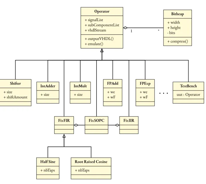
FloPoCo is also an extensive operator library which is already developed in the generator, and can be complemented by the designer’s own operators. A comprehensive list of the available operators can be found on the project’s homepage*. The class hierarchy is also briefly presented in Figure 2.11.
From a designer’s perspective, there are two main points of interest in FloPoCo: operators and targets. Most of the code of the FloPoCo framework is dedicated to operators, while the devices on which these operators can run on are abstracted as targets [37].
Operators (such asIntAdder,IntMultiplier,FixFIRetc.) model the flow of information in hardware datapaths, while targets (such asVirtex6,Kintex7,StratixVetc.) model the underly-ing hardware. The two work in conjunction. Thus, FloPoCo offers an opportunity in terms of the design process: the use of target-specific parameters during datapath creation . These parameters cover both the available hardware and the timing inside the datapath. Using this information, it is possible to create operators that are optimized for a given target and a given context.
Operator + signalList + subComponentList + vhdlStream + outputVHDL() + emulate() Shifter + size + shiftAmount IntAdder + size IntMult + size FPAdd + we + wF FPExp + we + wF TestBench uut : Operator FixFIR Half Sine + nbTaps
Root Raised Cosine + nbTaps
FixSOPC FixIIR
. . .
Figure 2.11:Par al Class diagram for the FloPoCo framework. Accent is put on the operators of interest to the work
presented in this thesis.
The rest of Section 2.3 deals with these two building blocks of the FloPoCo framework. Section 2.3.3 presents in more details the process of arithmetic datapath design, illustrated by constructing a toy operator. Section 2.3.4 presents concepts related to targets and how they influence a operator’s design.
Operators
FloPoCo arithmetic operators are hardware implementations of mathematical functions. They range from very basic ones like + and×, to trigonometric functions (sin, cos, atan), elementary functions (log, exp), to more complex ones like filters and polynomial approximations. From an architecture
point of view, they can be constructed as stateless (memoryless), combinatorial circuits†. From an arithmetic point of view, on the other hand, the operators are (in most cases) numerical approxima-tions of the actual mathematical funcapproxima-tions. Figure 2.12 shows an example of a mathematical function and its corresponding FloPoCo operator. The conceptual differences between the two (such as the domain for the inputs/outputs) are visible in the figure. Figure 2.13 shows another example, where the output of the operator is an approximation of the true mathematical result, on the target output precision.
+
x∈ R
y∈ R
r = x + y∈ R
(a)A mathema cal func on
+
X Y R / (16, 0) \ (16, 0) / (17, 0)(b)An operator with fixed point inputs and outputs
Figure 2.12:Example of a mathema cal func on and its corresponding FloPoCo operator
Figure 2.10 shows that the functional specification and the performance specification of a FloPoCo operator are separated. This is a design paradigm that has existed in FloPoCo since its early versions [37].
sin
x∈ R r = sin(x)∈ R
(a)A mathema cal func on
sin X R s.t.|R − sin(X)| ≤ 2−16 / (0,−15) / (0,−15) (b)An operator
Figure 2.13:Example of a FloPoCo operator approxima ng a mathema cal func on
An operator’s initial design phase is usually only concerned with the implementation of the func-tional specification. The implementation of the performance specification is left to further design iterations. These modifications should not impact the functionality of the operator, which might have already been tested and certified by this point. The main optimization is the pipelining of the datapath. This topic is introduced with the help of an example in Chapter 3 and discussed in more detail in Chapter 4, after a presentation of the state of the art in Section 3.3.
Targets
TheTargetclass tries to model the target hardware platform, in terms of timing and architectural
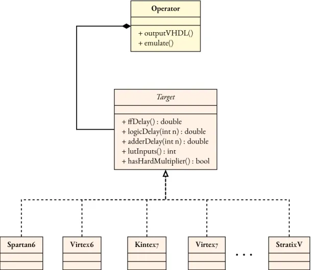
resources. Examples of how to integrate targets in the design of an operator’s datapath are provided in the listings of Chapter 3. The class diagram of theTargetclass is shown in Figure 2.14. Some of the details related to the hierarchy of theOperatorclass have been left out, for the sake of the clarity.
Operator + outputVHDL() + emulate() Target + ffDelay() : double + logicDelay(int n) : double + adderDelay(int n) : double + lutInputs() : int + hasHardMultiplier() : bool
Spartan6 Virtex6 Kintex7 Virtex7 StratixV
. . .
Figure 2.14:Class diagram for the FloPoCo framework with focus on the Target hierarchy
TheTargetclass provides information on the delays of the various elements of the datapath of
a FloPoCo operator. For example, a call toDSPMultiplierDelay()method the theTargetclass provides the delay of a hard multiplier block. The granularity of the information provided by the
Targetcan be very fine, such as the delay of a look-up table (LUT), or of a wire, or of a multiplier
block as in the previous example. The granularity can also be coarser. For example, the call to the
On the architecture side, theTargetclass abstracts details about the target device, that the de-signer can use inside its operators. For example, thelutInputs()method returns the number of inputs to the look-up tables (LUTs) on the target platform. The presence or the absence of certain capabilities in the hardware is also modeled in theTargetclass’ methods and attributes.
TheTargetclass can also abstract timing information on the various parameters of the target
platform, for use in the design of a datapath. Such methods exist for most of the elements that can be found in a target device. Thus, theTargetclass allows the designer to create generic datapaths, which produce operators tailored specifically to the target device and the target constraints.
As pointed out in [37], constructing models for target devices is a perpetual effort. On the one hand, there are always new devices to model and add to the supported library. On the other, the tim-ing information used for emulattim-ing the target devices is obtained from the evolvtim-ing vendor-provided tools. This means that:
• theTargetmodels are inherently approximate • theTargetmodels are constantly evolving
The structure and design of theTargetclass is in accordance to the paradigm used by the FPGA design suites. The class spans a large range of granularity for the level of control it provides to the designer. Experienced users can model their datapaths very precisely. This is in sync with the tools, which provide the necessary feedback so as to extract the information required to model theTarget
classes. However, there currently is a shift in the paradigm used by most of the vendor design suites. It is becoming increasingly difficult to predict the behavior and possible optimizations done by the synthesis/placement tools. In accordance, the evolution of theTargetclass, and the new design paradigm which it entails, is further discussed in Chapter 4.
Part I
Automatic Pipeline Generation for
Arithmetic Operators
Part I introduces the typical design flow for a FloPoCo operator , as well as how the operator’s frequency can be improved through pipelining. Chapter 3 presents the basics of creating an op-erator’s datapath with the use of an example (aMultiply-Accumulate unit). It also gives an overview of the current state of the art solutions for inferring pipelines inside arithmetic operator generators. Chapter 4 deals with FloPoCo’s new automatic pipeline generation framework. Finally, Chapter 5 discusses another new automatic feature of FloPoCo, the hardware resource consumption estimation.
The bi est difference between time and space that you can’t reuse time.
Merrick Furst
3
Operators and Pipelines
Lexicographic Time
This Section introduces a few notions related to timing and the system used by the pipelining frame-work for ordering signals inside a datapath.
Inside a combinatorial circuit, the timing of signals can be determined by accumulating the delays on simple paths to inputs. The timing of a signal is given by the longest (in terms of accumulated delay) such path.
Inside a pipelined circuit, however, the timing of a signal is usually given in a lexicographic system by a pair (c,τ). The cycle c is an integer that counts the number of registers on the longest path from the input with the earliest timing to the respective signal. The critical pathτ is a real number that represents the delay since the last register.
Signals can be ordered in a lexicographic order using the following relationship. A signal s1, with timing (c1,τ1), is before a signal s2, with timing (c2,τ2), if
(c1,τ1) < (c2,τ2) ⇐⇒ c1< c2 or c1= c2 and τ1<τ2 (3.1)
Another important notion required for the scheduling algorithm is that of lexicographic time addition. For a target frequency f , the corresponding cycle latency is 1/ f . The addition between a
∗
z∈ R
y∈ R x∈ R
+
r = z∗ y + x ∈ R(a)The mathema cal func on
∗
Z Y X+
R / wIn / wIn / wOut / 2∗ wIn T / 2∗ wIn (b)The operatorFigure 3.1:Example of a mul ply-accumulate unit
pair (c,τ) and a time delay δ is defined as:
(c ,τ) + δ = ( c + ⌊ τ + δ δob j ⌋ , τ + δ δob j − ⌊ τ + δ δob j ⌋) (3.2) In Equation 3.2,δob jis defined asδob j = 1/ f − δf f, whereδf fis the time delay of a register and f is the user-specified target frequency, with the corresponding cycle latency of 1/ f .
The addition between a lexicographic pair (c1,τ1)and another one (c2,τ2)can be performed as:
(c1,τ1) + (c2,τ2) = (c1 + c2,τ1) + τ2 (3.3)
which can further be reduced by using Equation 3.2. This is a sequential composition of operators.
Pipelining in FloPoCo 4.0
In the following, an example circuit is going to be built so as to give an idea of the design flow for an arithmetic operator in FloPoCo, as well as to illustrate the intricacies of the process. The cho-sen design is an example taken from the FloPoCo developer’s manual*, and describes a multiply-accumulate unit (MAC). A block schematic of the operator is presented in Figure 3.1.
Most of the code used for generating the datapath of an arithmetic operator is found inside the operator’s constructor, as illustrated by the example of Listing 3.1. An exception to this remark is represented by code reuse and factoring through methods, macros, auxiliary classes etc..
Every datapath in FloPoCo is an operator . Thus, the core class of the generator is theOperator
![Figure 2.2: Architecture and die of a Xilinx Virtex 7 chip. Image extracted from [6].](https://thumb-eu.123doks.com/thumbv2/123doknet/14590316.730057/25.892.160.803.668.931/figure-architecture-die-xilinx-virtex-chip-image-extracted.webp)
![Figure 2.5: Organiza on of logic resources on Intel devices. Image extracted from [9].](https://thumb-eu.123doks.com/thumbv2/123doknet/14590316.730057/29.892.165.786.153.591/figure-organiza-logic-resources-intel-devices-image-extracted.webp)
![Figure 2.6: Overview of an ALM on Intel devices. Image extracted from [9].](https://thumb-eu.123doks.com/thumbv2/123doknet/14590316.730057/30.892.121.715.155.611/figure-overview-alm-intel-devices-image-extracted.webp)
![Figure 2.7: Overview of a DSP slice on Xilinx devices. Image extracted from [5].](https://thumb-eu.123doks.com/thumbv2/123doknet/14590316.730057/31.892.170.782.153.483/figure-overview-dsp-slice-xilinx-devices-image-extracted.webp)
![Figure 2.8: Overview of a Variable Precision DSP Block on Intel devices. Image extracted from [10].](https://thumb-eu.123doks.com/thumbv2/123doknet/14590316.730057/32.892.123.729.165.419/figure-overview-variable-precision-block-intel-devices-extracted.webp)