Controlled fabrication of nanoscale gaps using stiction
The MIT Faculty has made this article openly available. Please share
how this access benefits you. Your story matters.
Citation
Niroui, Farnaz, Ellen M. Sletten, Parag B. Deotare, Annie I.
Wang, Timothy M. Swager, Jeffrey H. Lang, and Vladimir Bulovic.
“Controlled Fabrication of Nanoscale Gaps Using Stiction.” 2015
28th IEEE International Conference on Micro Electro Mechanical
Systems (MEMS) (January 18-22, 2015), Estoril, Portugal.
As Published
http://dx.doi.org/10.1109/MEMSYS.2015.7050892
Publisher
Institute of Electrical and Electronics Engineers (IEEE)
Version
Author's final manuscript
Citable link
http://hdl.handle.net/1721.1/108573
Terms of Use
Creative Commons Attribution-Noncommercial-Share Alike
CONTROLLED FABRICATION OF NANOSCALE GAPS USING STICTION
Farnaz Niroui, Ellen M. Sletten, Parag B. Deotare, Annie I. Wang,
Timothy M. Swager, Jeffrey H. Lang, and Vladimir Bulović
Massachusetts Institute of Technology, Cambridge, Massachusetts, USA
ABSTRACT
Utilizing stiction, a common failure mode in micro/ nano electromechanical systems (M/NEMS), we propose a method for the controlled fabrication of nanometer-thin gaps between electrodes. In this approach, a single lithography step is used to pattern cantilevers that undergo lateral motion towards opposing stationary electrodes separated by a defined gap. Upon wet developing of the pattern, capillary forces induce cantilever deflection and collapse leading to permanent adhesion between the tip and an opposing support structure. The deflection consequently reduces the separation gap between the cantilever and the electrodes neighboring the point of stiction to dimensions smaller than originally patterned. Through nanoscale force control achieved by altering device design, we demonstrate the fabrication of nanogaps having controlled widths smaller than 15 nm. We further discuss optimization of these nanoscale gaps for applications in NEM and molecular devices.
INTRODUCTION
As dimensions are continuously scaled down to achieve electronic, photonic and electromechanical devices with improved performance and novel principles, developing methods for the controlled fabrication of electrodes separated by nanometer-thin gaps is important to enabling reliably-functioning devices. Current methods of fabricating such nanogaps include oblique-angle shadow evaporation, electrochemical deposition, electromigration, mechanical break junctions, molecular junctions and etching of nanometer-scale sacrificial layers [1-5]. However, these approaches, mainly developed for two-terminal devices, commonly involve multiple processing steps and lack robustness and tunability, thus preventing effective incorporation into more complex multi-terminal designs. These limit their practical applications in integrated systems.
A common mode of failure in electromechanical systems is permanent adhesion between device components, referred to as stiction. Stiction arises due to the surface adhesion forces overcoming the elastic restoring force of a mechanically active structure, leading to its collapse and hindering its recovery. As surface adhesion forces increase with the decrease in gap dimensions, stiction becomes increasingly more challenging in NEM devices.
Here, we propose the use of stiction, typically considered an irreversible failure mode, to promote controlled fabrication of electrodes separated by nanoscale gaps of varying widths. The feasibility of this approach to form nanogaps with dimensions smaller than 15 nm, and their potential applications are investigated in this paper.
DESIGN PRINCIPLES
Capillary forces exerted on the mechanically-active structures of electromechanical systems by the drying of the liquid trapped in the small gaps of the devices after wet fabrication processing can readily lead to stiction [6]. Taking advantage of this stiction, our proposed method of fabricating nanogaps relies on control of the surface adhesion forces at the nanoscale to enable control of cantilever deflection that is used to tune the gap. The laterally-actuated cantilever and other device components are fabricated through a one-step lithography process. During the wet developing of the patterned structures, capillary forces induce deflection and eventual collapse of the cantilever. The stiction between the cantilever and a support structure enables formation of gaps smaller than originally patterned between the cantilever and additional electrodes located relative to the point of stiction. Through changes to the structural design and liquid phase processing step, surface adhesion forces caused by the capillary action can be adjusted to allow for precise control of the gap size.
FABRICATION
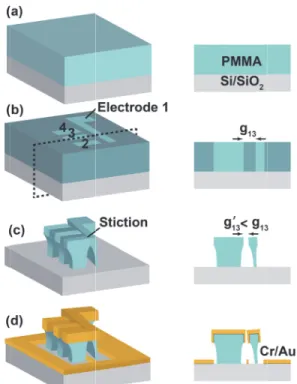
The fabrication scheme for stiction-induced formation of nanogaps is shown in Figure 1. Five layers of poly(methyl-methacrylate) (PMMA), a positive electron beam resist, are spun over a silicon (Si) substrate with 2 µm-thick thermal oxide (SiO2). Each layer is spun at 2000 rpm
for 45 s and baked at 180 oC for 90 s. The initial three
layers of PMMA have molecular weight of 495 kg/mol (PMMA 495 A6) and the following two layers have molecular weight of 950 kg/mol (PMMA 950 A4). Next, the cantilever and other electrodes are defined by patterning the PMMA film using electron-beam (e-beam) lithography. The resist is developed in 1:3 dilution of methyl isobutyl ketone (MIBK) in isopropanol for 3 min, placed in an isopropanol bath to thoroughly rinse, and dried under a gentle stream of nitrogen normal to the surface. Finally, about 10 nm of chromium (Cr) and 100 nm of gold (Au) are deposited over the substrate using thermal evaporation to form the electrodes.
The five layers of PMMA of two different molecular weights with a total thickness of about 1.5 µm allow fabrication of large aspect ratio features with an undercut profile, a thinner base and a thicker top section. The undercut is achieved due to the differential dissolution rate of PMMA of varying molecular weights in MIBK; lower molecular weight PMMA has a faster dissolution rate than the higher molecular weight PMMA. The undercut prevents sidewall coverage during metal deposition and ensures electrical isolation between the electrodes. The undercut and the high aspect ratio of the PMMA cantilever also
e e f la c ( s e f n c g T c d c m e s
R
s in o c a d li e p li a m d c p th th a ~ th in c o c F to s d n li s b renable the struc During the exerted on the force can cause arge to overco collapses on t (Electrode 2) a stiction reduce electrodes posit from the poin nanogaps sma constant of the geometry and t Then, by adju control the ex desired gap dim can further be r metal onto the electrodes. The step is depende
RESULTS A
The feasib smaller than pa n Figure 2. T overcome the causing the ir altering the des dimensions of t iquid used, th ensure collaps processing. Th imited to the approach. Sim materials other different materi controlling the process [8]. In he scheme in he gap size be approximately ~50 nm betwee he stiction reg n a similar can Through e cantilever, and opposing elect controlled. An Figure 3. Figu o ~10 nm by p stiction. The demonstrated in nm to 170 nm imited to two same lithograph be fabricated. relevant to ap cture to freely d e wet-developin cantilever (E e deflection of ome the spring to an opposin and undergoes e the gap betwtioned along th nt of stiction, aller than orig
e cantilever ca the relative po usting the surf tent of deflec mensions are ac
reduced in size PMMA struc e reduction in ent on the thick
AND DISCU
bility of utilizin atterned in a si To promote stic elastic restor rreversible co sign and proce the cantilever, he surface adh se of the acti he nanogap fab material sets milar results than PMMA a ials selections e surface adh n the cantileve Figure 1, stict etween Electrod 30 nm. Once en Electrodes gion is achieve ntilever that hasengineering o the geometry trodes, the si n example ~35 ure 3b illustrate positioning Ele tunability of n Figure 4 whe m are formed. o-terminal stru hy step, device These mul plications in deflect due to a ng process, a c lectrode 1) in f the cantilever g restoring forc ng PMMA s s stiction. Th ween the cant he length of the leading to th ginally pattern an be adjusted sitioning of co face adhesion ction and its p chieved. The f e by evaporati ctures to define
gap size durin kness of the dep
USSION
ng stiction to d ingle lithograp ction, the capil
ring force of llapse of the essing conditio the patterned esion forces c ive structure brication presen used in our are expected and Au are use provide an add esion forces er of Figure 2, tion is promote de 1 and Elect e collapsed, an 1 and 3 at the d compared to s not undergon f the spring y and relative p ize of the na nm gap fabric es the reductio ectrode 3 close
the gap dime ere gaps rangin As shown, th uctures. Furth es with multip lti-terminal de integrated sys an applied forc capillary force Figure 1. Th r. If sufficien ce, the cantilev support structu he deflection a
tilever and oth e cantilever aw he formation ned. The spri
d by altering ounter electrod forces, one c profile such th formed nanoga ing a thin-film e the conducti ng this processi posited film. develop nanoga hy step is show llary forces mu f the cantilev structure. B ns, including t gap size, and t can be altered during the w nted above is n proof-of-conce in cases whe ed. Furthermo ditional means
and the sticti fabricated usi ed by decreasi trodes 2 and 3 effective gap e point closest o the 200 nm g ne stiction. constant of t placement of t anogaps can cated is shown on in the gap si er to the point ension is furth ng from about he process is n her, through t le electrodes c evices are mo stems and allo
Figure than pa a canti cantilev capilla leading Figure stiction Si/SiO2 pattern electro develop isoprop ~10 nm pattern ce. e is his ntly ver ure and her way of ing its des. can hat aps of ive ing aps wn ust ver, By the the to wet not ept ere ore, of ion ing ing by of to gap the the be in ize of her 10 not the can ore ow 2: Stiction pr atterned; (a) S ilever with a g ver positioned ary force in (b g to stiction an e 1: Controlled n; (a) multilay 2 substrate an
ned using e-be odes separated ped in 1:3 solu panol bath and m of Cr and ~ ned structures d romotes format Scanning electr gap of ~200 n d closer to ele (b) causes col nd reducing the d fabrication o yer PMMA e-b nd baked after eam to define d by a defined ution of MIBK d dried under ~100 nm of Au
defining the ele
tion of nanoga ron micrograph m, (b) SEM of ctrodes 2 and llapse of the e gap between 1 of nanoscale g beam resist is r each spin, (b cantilever and d gap “g”, (c in isopropano a stream of ni u is evaporate ectrodes. aps smaller h (SEM) of f the same d 3. Larger cantilever, 1 and 3. gaps using spun onto b) resist is d opposing c) resist is l, rinsed in itrogen, (d) ed onto the
F F p f E p F p n v e f w s t s a Figure 3: SEM Figure 1. Cap pattern cause forming a gap Electrodes 1 a positioning Ele Figure 4: Op placement rela nanogaps with various multi-t exploration of m A potenti fabrication sche which, with t switching and echnology com semiconductor actuation voltag M of nanogaps f pillary forces stiction betwe p of ~35 nm and 3. The sma
ectrode 3 close timizing devic ative to the po h controlled w terminal device more complex ial application eme is in the d their large on near-zero leak mpetitive with transistors [8] ges is among t fabricated usin during wet de een Electrodes (a) and ~10 n aller gap in (b) er to 2. ce architecture int of stiction width, useful fo es. device designs n of the pro development o n-to-off curren kage currents h h complementa . However, th the main challe
ng the scheme eveloping of th 1 and 2, whi nm (b) betwee b) is achieved b e and electrod allow achievin or fabrication s and concepts oposed nanog f NEM switch nt ratios, abru have emerged ary metal-oxid he need for lar
enges preventi in he ile en by de ng of Figure smaller be fab (blue c switche bottom (b) Pro . gap es, upt as de-rge ing integrat reduce switchi electros nanoga been a size of devices fabricat stiction device remain applied more modula current bias. T through approac switche transist Na applica molecu formed metallic fragile workin Throug damage molecu formati liquid-p functio attachm 5: (a) Throug r gaps and mo bricated to un compared to r es. Insets sho cantilever (bl ototype design tion of NEM s
the operating ing gap is nece
static force o ap size to the fundamental f f the switching s lowers due to tion. In con n is used to ben design, the stationary or d voltage. As s flexible ca ation of the g t modulation o The desired sw h the optimizat ch can also b es that more tors. A prototy anogaps have ations in mole ule-metal junct d using techn c contacts, wh organic mole ng devices an gh the proposed e to the mol ules are intro ion through te phase self-asse onalized with ment onto th gh altering dev ore flexible ca ndergo electro red), useful fo ow correspon lue) ~20 nm th of a three-term switches into w g voltage, dec essary, as it le of actuation. few-nanomete fabrication cha g gap decreases o failure mode ntrast, in our nefit nanogap f collapsed elec r undergo mec shown in Figu antilever all gap. In this of 1011 is achie witching perfo tion of the fab be extended t closely rese ype design is sh e also been ecular electron tions. These niques such a hich has the ecular layer, le nd structures d stiction-indu lecular layer oduced into t echniques such embly. In self terminal grou he electrode vice geometry antilevers, nan omechanical m for application nding devices hinner than the minal NEM swi widely used sy rease in the s eads to an incr The reductio er regime, how allenge. Typic s, the yield of es such as stict proposed app formation. Dep ctrode can be chanical motio ure 5, a smaller low electrom two-terminal eved within 3 ormance can b brication techn to three term emble the co hown in Figure n widely de nics that rely gaps are conv as direct dep potential to d eading to low that lack r uced nanogap f can be avoid the gap after h as vapor dep f-assembly mo ups that enable
surfaces. For to achieve nogaps can modulation ns in NEM with the e top (red). itch. ystems. To size of the ease in the on of the wever, has ally, as the f functional tion during proach the pending on e made to on with an r gap and a mechanical example a V applied e achieved ique. This minal NEM onventional e 5b. esired for on metal-ventionally position of damage the w yields of robustness. fabrication, ded as the r electrode position or olecules are e selective r example
F o d R N d th s d s d o in n e f th c to o f f c S s g a e u a th d s th
C
g f in d T p Figure 6: The of different s decanethiols s Representative Nanogaps of d design while ch hiolated molec shows the cur different sizes self-assembled deposition. As observed with nterpretation o nature of the experimentation formed, furthe hrough chang changes in surf o form anti-st operation reliab for quantum tun Although fabrication of n challenges that SEM images, th surface roughn gap size, makes and can alter de exploring mate use of techniqu atomically smo hat require na different mate structures requ hat may increaCONCLUSI
A method gaps is propose failure in ele nduced during deflection of a The deflection patterned. The current-voltag izes with mo self-assembled e SEM image different sizes hanging the siz cules self-asse rrent-voltage c with thin-film on the Au expected, a h the decre of the data to molecular jun n. We specula er decrease in ges in surface face properties. tiction coating bility, and to f nneling NEM s providing nanogaps, the p must be addre he as-deposite ness, which ints the devices su evice performa rials alternativ ues such as at ooth surfaces. nogaps with a erials can be uires modificat
ase its complex
ION
for controlled ed that utilizes ectromechanica g liquid phase p a movable elec leads to redu e experimental ge characterist lecular layers d on the Au e of the device are achieved ze of original g emble onto go characteristics ms of fluorin surface usin general increa ease in gap extract inform nction require ate that as mol n gap size c adhesion for . This approach s in NEM dev form molecula switches [10]. a promising proposed techn essed. As obse d metal electro troduces inhom usceptible to e ance. This can ve to Au and PMtomic layer de In addition, fu asymmetric me envisioned. ions to the fab xity.
fabrication of s stiction, a co al systems. C
processing of t ctrode and con uction in the l results suppo
ics of three gap s of fluorinate electrodes (lef es tested (righ using the sam gap patterned. old [9]. Figure of nanogaps ated decaneth ng vapor pha ase in current size. Furth mation about t es more detail lecular layers a can be achiev rces imposed h is also valuab vices to enhan ar switching ga platform f nique faces som erved through t odes have a lar mogeneity in t electrical shorti n be overcome MMA or throu eposition to for unctional devic etal electrodes Enabling su brication schem f nanometer-sca ommon source Capillary forc the sample cau nsequent stictio size of the ga ort the feasibil
ps ed ft). t). me e 6 of hiol ase is her the led are ved by ble nce aps for me the rge the ing by ugh rm ces of uch me ale of ces use on. aps lity of the control enginee of this develop electrom
ACKN
Th Founda Science the sup CounciREFE
[1] H. thr mo 01 [2] T. Ma [3] F. S R. of film [4] J. O Yo dev [5] D. Am deM ele Co [6] O. “In ME 10 [7] M. On pla eff [8] O. con 29 [9] J. C M. thi Ch [10] F. Ya “N sel Int SysCONT
*F e proposed m lled widths s ering of surfac s versatile fa pment for mechanical andNOWLEDG
his work is ation (NSF) C e (E3S) Award pport of Natur il of Canada (NERENCES
B. Akkerman rough single onolayers”, J. 3001, 2008. Li, W. Hu, ater., vol. 22, p Streller, G. E. W. Carpick, platinum silic ms”, Adv. Mat O. Lee, Y. Song oon, “A sub-1vice”, Nature N J. Beesley, massian, M. A Mello, “Sub-1 ectrodes and d ommun., vol. 5, Raccurt, F. Ta nfluence of liq EMS”, J. Micr 90, 2004. Toda, A. Yo no, “Fabricatio astic deformat fects”, Microsy Y. Loh, H. ntact switches 5, 2012. C. Love, L. A. . Whitesides iolates on me hem. Rev., vol.
Niroui, P. B. ablonovitch, T Nanoelectromec lf-assembled ternational Co stems, pp. 1103
TACT
F. Niroui, tel: + method to fab smaller than ce adhesion for fabrication pla various a d molecular deGEMENTS
supported by Center for Enerd ECCS-0939 ral Sciences an NSERC). n, B. de Boer e molecules Phys.: Con D. Zhu, “Nan pp. 286-300, 20 Wabiszewski, “Tuanble, sou ides and nano ter. Interfaces, g, M. Kim, M. -volt nanoelec Nanotech., vol J. Semple, A. McLachlan, 15-nm patterni devices by adh , 3933, 2014. ardif, F. Arnau quid surface te romech. Micro okoyama, N. V on of nano-g tion of straine yst. Technol., p D. Espinosa, s”, Nature Nan Estroff, J. K. K s, “Self-assem etals as a for 105, pp. 1103-Deotare, E. M . M. Swager, chanical tunne molecular onference on M 3-1106, 2014. +1-617-324811 abricate nanog 15 nm, thr rces. Further op atform allows applications evices. y the Nationa rgy Efficient E 514. F.N. ack nd Engineering r, “Electrical c and self-ndens. Matter, nogap electro 010. , F. Mangolini urce-controlled gaps from thin , vol. 1, 130012 Kang, J. Oh, H ctromechanical l. 8, pp. 36-40, L. K. Jagad T. D. Anthopo ing of asymme hesion lithogra ud d’Avitaya, ension on sticti oeng., vol. 14, V. Toan, N. In gap structures d Si springs b pp. 1-6, 2014. “Nanoelectrom notech., vol. 7 Kriebel, R. G. mbled mono rm of nanotec -1169, 2005. M. Sletten, A. I J. H. Lang, V eling switches layers”, IE Micro Electro M 0; fniroui@mi gaps, with rough the ptimization s nanogap including al Science Electronics knowledges g Research conduction -assembled , vol. 20, des”, Adv. i, G. Feng, d formation n precursor 20, 2014. H. Yang, J. l switching 2013. damma, A. oulos, J. C. etric metal aphy”, Nat. T. Varine, ion of SOI , pp. 1083-nomata, T. based on by stiction mechanical 7, pp. 283-Nuzzo, G. layers of chnology”, . Wang, E. V. Bulović, s based on EEE 27th Mechanical it.edu