Cryogenic Characterization of Josephson Junctions
by
Keith Andrew Brown
Submitted to the Department of Physics
in partial fulfillment of the requirements for the degree of
Bachelor of Science in Physics
at the
MASSACHUSETTS INSTITUTE OF TECHNOLOGY
May 2006
( Massachusetts Institute of Technology 2006. All rights reserved.
A uthor ...
... ...
...
Department of Physics
May 18, 2006
Certified
by...
Leonid Levitov
Professor
- -~-/7 Thesis Supervisor
William D. Oliver
MIT Lincoln Laboratory
Thesis Supervisor
Accepted
by ...
... .
.. ...
David E. Pritchard
Senior Thesis Coordinator, DeDartment of Physics
ARCHIVES
MASSACHU8sE-rs SSItE
OF TECHNOLOGY
Cryogenic Characterization of Josephson Junctions
by
Keith Andrew Brown
Submitted to the Department of Physics
on May 18, 2006, in partial fulfillment of the requirements for the degree of
Bachelor of Science in Physics
Abstract
Cryogenic characterization is a crucial part of understanding the behavior of low-temperature quantum electronics. Reliable device testing provides the feedback to fabrication process development, facilitating the rapid development of quantum de-vices. The research presented in this thesis explores the cryogenic testing, analysis, and characterization of a superconducting quantum device, the Josephson junction. This thesis begins with a theoretical description of superconductivity and Josephson junctions, two superconductors separated by a thin insulating battier. Two models of
Josephson barriers are presented for use in analysis. The effect of self-induced mag-netic field is considered. A numerical simulation is performed to justify neglecting effects of self-induced magnetic field in junctions of diameter less than the Josephson penetration depth Aj. Lincoln Laboratory's Josephson junction fabrication effort is described along with the apparatus used to test junctions at 4.2 K. Custom soft-ware used to test these junctions is then presented. The analysis of 4.2 K data is shown with a simple model of a disc as the insulating barrier. 391 valid Josephson junctions are analyzed across 16 wafers in 3 runs. The critical current density J is
calculated to be 4.88 i 2.81 ( 2) for junctions with expected J of 5 (A2). The superconductive energy gap A is calculated to be 1.51 ± 0.31 meV. The process bias 60 is shown to be -0.35 i 0.12 ,tm. Analyzing the junctions with an alternate model
taking into account pollution produces an upper bound for barrier pollution depth
of approximately 60 nm. Discussion of a 300 mK apparatus is then presented. This apparatus is constructed and presently being incorporated in an existing 300 mK 3He
refrigerator. Finally, the results are concluded with a discussion of advantages, and proposed initial experiments for the 300 mK apparatus.
Thesis Supervisor: Leonid Levitov Title: Professor
Thesis Supervisor: William D. Oliver Title: MIT Lincoln Laboratory
Acknowledgments
I would like to acknowledge many people for their contributions to my thesis. First, my advisor at Lincoln Laboratory, Dr. William Oliver, has been extraordinarily helpful and patient. I owe him my deepest gratitude for his continual help and advice about this thesis and more. Terry Weir, Robert Konieczka, and JoAnne Rantz have been very helpful, and I thank them for their technical help, advice, and company. I would like to thank Vladimir Bolkhobsky for his help as well. On campus, Prof. Terry Orlando was very helpful and welcoming as I worked through the simulation. I would like to thank Janice Lee for her help with theory. David Berns deserves my thanks for his patience and help with laboratory and apparatus design. Prof. Leonid Levitov also deserves my thanks for his feedback on my thesis. I would also like to thank the MIT machine shop and Peter Morley in particular for their patience in dealing with someone who had never done design before. I would like to thank peers who helped me through technical difficulty, Mike Wolf, Victor Brunini, Sam Raymond and Matthew Drake. Finally I would like to thank my friends and family
that sympathized and supported me during this project.
Contents
1 Theory and Motivation
1.1 Motivation .
1.2 Superconductivity. ...
1.3 The Josephson Equations ...
1.4 Relation of Shape to Critical Current . . 1.5 Self-Limiting Induction Effects .
17 ... ...17 ... ...18 ... .. 21...
... .. ...
24
... .. ...
26
2 4He Josephson Junction Characterization 29 2.1 The Junctions ... 29
2.2 Apparatus Description . . . ... 31
2.3 Characterization of Josephson Junctions ... 33
2.4 Analysis of Wafers ... 37
3 4He Cryogenic Results 39 3.1 Energy Gap Determination . . . ... 39
3.2 Critical Current and Process Bias ... 40
3.3 Barrier Pollution Analysis ... 43
4 Apparatus for 3He Refrigerator 47 4.1 Battery Boxes ... 47
4.2 Switching Matrix ... 49
4.3 High Precision Instrumentation Amplifier ... 50
4.5 300 mK Electronics ... 55 4.6 Other Room Temperature Electronics . . . ... 56 4.7 Testing Room Temperature Apparatus ... 57
5 Future Plans and Concluding Remarks 59
5.1 Summary ... 59
5.2 Future Plans ... 60
A Figures 63
B MatLab Code 75
B.1 Self-Limiting Induction Effects ... 75 B.2 Characterizing Josephson Junctions ... 77
List of Figures
1-1 (Left) Sample I-V traces of a Josephson junction at different temper-atures with fetemper-atures relevant to analysis labeled. The blue curve
cor-responds to T = 0 K and the red curve corcor-responds T > T > 0.
(Right) Energy diagram of a Josephson junction with applied voltage V. Thermal excitations have put some electrons in the quasiparticle regime. For as long as there can be supercurrent, as governed by equa-tion (1.16), there is no voltage gap. As soon as the applied current exceeds J, voltage between the two superconductors jumps up until
the superconducting band of one is level with the normal band of the
other. This allows for quasiparticle tunneling. This persists even when the voltage is then reduced, because there are still electrons excited that will continue to tunnel resulting in a subgap voltage ... 23
1-2 Diagram of the Josephson junction barrier model being analyzed. This analysis is most convenient in cylindrical coordinates ... 25
1-3 (Left) Dimensionless plot of maximum current against Josephson junc-tion radius. The two lines are indistinguishable until nearly 2AJ.(Right) Calculated starting value of used at s = 0 to give the maximum value of I,. The curve originating at is expected because in small junctions the self field doesn't have a big effect so the current can be maximum everywhere. As the size increases the starting value goes to 0, which
2-1 (Left) This diagram shows the materials that make up a Josephson Junction in the Niobium trilayer junctions. The diagram is not to scale. (Right) A scanning electron microscope image of the pillars that will form Josephson Junctions. These are very small junctions,
approximately 0.2 /um in diameter. ... 30
2-2 4.2 K Peterson testing apparatus. The oscilloscope is connected to a computer that is used to control readout and record the data. .... 32
2-3 Current voltages traces of two working junctions. These are direct output plots of the program. The second shows two artifacts of the data collection method. The presence of two distinct lines in the sub gap regime is because of the averaging, and the slight jump close to the negative knee is a mistake that comes from stopping data collection while the current is still sweeping back and forth. ... 36
3-1 Histograms of measured A from two of the three runs. The gaussian is only used for purposes of reporting a mean and variance in mean for A. 40
3-2 (Left) Histogram and Gaussian fit of fitted die J from die of wafers with expected J of 5 $-. The gaussian is used for mean and error determination with results listed in table (3.2). (Right) Histogram and gaussian fit of the process bias of all die analyzed. The gaussian is used for mean and error determination with results in table (3.2). ... 43
4-1 A diagram of the 300 mK refrigerator fitted to analyze devices. Each component is discussed in more depth in Chapter (4). The voltage across the source resistor gives a current reading for the oscilloscope and the amplified voltage from the chip gives the voltage reading for
the oscilloscope. ... 48
A-1 A diagram of a test structure that shows the connecting pads for a single Josephson junction. The inset shows the relative scale of the
A-2 Graphical user interface (GUI) of the custom MatLab software devel-oped for the LTSE and DSM project. The drop box has two options of what to analyze, the two images show these two options. The check boxes control what the program analyzes and saves ... 64
A-3 Two failure modes of Josephson junctions that are caught by analysis. These are direct output plots of the program. The left junction is leaky, where resistive channels are present across the insulating barrier. The second is shunted. These failure modes are distinct but do not reveal exactly which fabrication problem they represent. The red points on the graph indicate points used for fitting ... 65
A-4 An example wafer map measuring critical current density. The blank squares indicate that either no chips were tested from that die or that there were not enough valid junctions to determine Jc ... 65 A-5 Plots of fitting averages across a single run. In these plots, LTSE05_1
is summarized. In the plots of average So and Jc the error bars signify the range of the value from each wafer. The expected J¢ was 5 'LA for
wafers 1 through 8 ... 66
A-6 A bar graph that shows distribution of junction type and failure mode by wafer number. This makes it clear what kind of failure modes were
dominant on each wafer. ... 67
A-7 A plot of the fitted V/ vs. 6. An entire wafer of data is shown here, with individual die differentiated by different colors and direction triangles. Triangles with a red 'x' inside them signify that the point was not used for fitting, either due to a of lack of points or it was determined to be an outlier. ... 67 A-8 Data from the DSM2_19_8 wafer. Every chip on the wafer was tested
and the yield was high, making it an ideal wafer to look at trends across the wafer. Error reported is error in linear fitting. Traits that are reported with zero error indicate only two functioning junctions,
A-9 Fitting residuals plotted against junction diameter. There are notice-able trends in the average residual for a given diameter. The residual would be centered about 0 if the noise was random ... 68
A-10 Histogram of the modified determinant with a gaussian fitted to it. The mean is -. 0010 .0079 m2. ... 69
A-11 Example of voltage vs. time plots from the output of the waveform generator and from the amplifier. While the input amplitude is the same for both plots, the phase is different because the measurements were taken at different times. The amplifier presents a 10 kQ load resis-tance, which greatly dominates the source resistance of 50 Q. Internal scope resistance of 1 MQ is used to get a similar load for the scope. . 70
A-12 Histogram and Gaussian fit of zero input voltage readings of the AD8221
amplifier ... 70
A-13 (Left) Histogram and Gaussian fit of zero input voltage readings of the AD8221 amplifier. (Right) Histogram of zero input voltage reading of the optical isolation amplifier. The voltages do not fit a gaussian, but the mean is 4 mV and the variance can be approximated by 6 mV. . 71
A-14 The top graph is the frequency ramped sine wave input to the amplifier. The bottom graph is the output of the amplifier. The The envelope of the bottom graph is the frequency response of the device ... 71
A-15 The top graph is the frequency ramped sine wave input to the optical isolation amplifier. The bottom graph is the output of the optical isola-tion amplifier. The The envelope of the bottom graph is the frequency
response of the device. ... 72
A-16 4.2 K Peterson testing apparatus modified with custom electronics for the purpose of verifying the electronics. Components in shaded boxes indicate that they were designed and tested for this project. ... 73
A-17 (Left) Current-voltage trace of a Josephson junction taken by the cus-tom apparatus described in figure (A - 16). (Right) Current-voltage
trace of the same Josephson junction taken by the apparatus described
in figure (2 - 2). ... 73
C-1 Electrical schematic of the battery circuit. A single voltmeter can be switched to read either polarity. Each battery circuit ground can be connected to the neighboring circuit's ground. ... 100
C-2 Design schematic of the physical battery box. Two complete batteries fit inside each box. A simple aluminum lid (not pictured) is attached to the top of the box to ensure electrical shielding. The box is designed to fit in a standard rack mount. ... .. 101
C-3 Design schematic of the thermal finger that holds the chip in place. The chip attaches to a small mount that screws onto the end of the finger. This both holds the chip in place and maintains a good thermal connection. The four holes through the finger are where the copper
powder filters attach ... 102
C-4 Design schematic for the box that holds the RC filter. A mini D-sub plug attaches to each side of the box. Two removable lids (not
pictured) attach to the top and bottom for access to the circuit boards.
The circuit boards mount back to back in the middle of the device for space conservation. . . . ... 103
C-5 Design schematic for the copper powder filters. Each unit holds six copper powder filters, each with a twisted pair running though it. The filters attach to the thermal finger via two screws ... 104
C-6 PC board design for the RC low-pass filter. Each of twelve channels has room for a resistor in series and a capacitor to ground. The back is a ground plate that rests on the device box ... 105
C-7 PC board design for the amplifier circuit. In addition to decoupling capacitors, the design also features single pole RC high-pass filters on the inputs. This eliminates DC noise. External connections enter through Molex connectors soldered onto the surface . ... 105 C-8 PC board design for the optical isolation circuit. The circuit has a
total of eight decoupling capacitors. There are three potentiometers used to trim various characteristics of the device. The chip itself fits inside an 18-pin dip connection for easy interchange. ... 106
List of Tables
3.1 Mean values of A for three runs. BCS predicted value for niobium is A(T=o) = 1.40 meV, from equation (1.10). This has been experi-mentally shown to be 1.55 meV, which is shown to be constant over
0.4- 4.2 K [25]. . . . 40 3.2 Typical values of fitting parameters from the linear model. For finding
J,, only junctions with expected J of 5 AA are used. For finding 60
all junctions are used . . . ... 43 3.3 Table of fit values for the quadratic fit y = ax2 + bx + c of I(6). .. 44
3.4 Summary of values from analysis. Some outliers were discounted in the range determinations, but only those that were clearly mistakes of fitting. These statistics encompass all 391 junctions used in analysis. 46
Chapter 1
Theory and Motivation
1.1 Motivation
The Josephson effect is the physical effect that describes tunneling between two super-conductors through an insulator i.e., a Josephson junction. The Josephson junction has been an important device in quantum electronics since it was predicted in 1962 by Brian David Josephson [1]. The properties of Josephson junctions and Josephson-based devices have made them of particular interest to the areas of precise magnetic sensing, quantum computing, superfluidity, and solid state physics. These proper-ties include extreme sensitivity to magnetic fields, a small voltage-free dissipationless supercurrent, and nonlinearity in resistance.
Josephson junctions have been used as constituents of Superconductive Quantum Interference Devices (SQUIDs) which are used to measure magnetic fields with very high sensitivity [2]. High resolution probes for detecting magnetic fields have been implemented with SQUIDs with spatial resolution of 10 Mm [3]. This has also been implemented in Niobium systems operated at 4.2 K [4]. SQUID based magnetic imaging has been used to detect nuclear magnetic resonance (NMR) and biomagnetic signals at ultra-low fields [5].
Josephson junctions can be used as the building blocks of logic elements for
Quan-tum Computation. Persistent current quanQuan-tum bits (qubits) are a convenient and
[6]. Multiple qubit systems have been fabricated out of charge-based and flux-based qubits comprised of Josephson junctions [7]
The Josephson effect has been observed in systems besides superconducting tun-nel junctions. Josephson effects have also been observed in carbon nanotubes [8]. Josephson-type dynamics are applicable to other superfluids. Bose-Einstein conden-sates also exhibit this type of behavior and this has been studied [9],[10]. Josephson junctions can also be used to study anisotropy in the superconducting energy gap, and it has been used to study the energy gap of lead [11].
MIT Lincoln Laboratory has a continuing effort to fabricate and test Josephson junctions and other superconducting circuit elements. This is contained in a push towards quantum computing and has collaboration with the Orlando group in MIT's Research Laboratory of Electronics. Research within this collaboration has a broad scope and encompasses many facets of superconductive electronics [6, 12, 13, 14].
Making devices with reliable properties requires the accurate characterization and analysis of Josephson junctions. This requires cryogenic testing and analysis of many junctions. The aim of this thesis is the characterization and analysis of Josephson
junctions. It encompasses the apparatus for taking data at 4.2 K, the methods for
characterizing junctions, the analysis of aggregate data, and finally the progress to-wards constructing a separate apparatus for testing these circuit elements at 300 mK.
1.2 Superconductivity
Before analyzing superconducting tunneling junctions, it is natural to begin with an overview of superconductivity. Unless otherwise cited, this background is borrowed from references [2] and [15]. Certain materials will exhibit characteristics of supercon-ductivity when it is cooled below a critical temperature T¢ that is dependant on the material. Below this temperature electrons will pair together to form Cooper pairs, which behave as bosons. These pairs form a many particle wave function which has phase coherence over macroscopic distances. Each electron of a Cooper pair exists at
an energy below the Fermi surface of A(T). This is known as the superconducting
energy gap and it is a temperature dependant property of the material.
Superconductivity was originally described by the London equations:
Et= s (1.1)
and
B
=-Vx
LJ
(1.2)
AL is known as the London penetration depth; it is a temperature dependant property
of the material and will be discussed later. Equation (1.2) can be combined with the Maxwell equation for curl of a magnetic field to yield the second order-equation,
2~
B
V2B= (1.3)
Superconductive materials exhibit two important characteristics that follow from the London equations. Like perfect conductors, they have no resistance (perfect conduc-tivity). This follows from equation (1.1). Resistance is related to the proportionality in Ohm's law of electric field to velocity. In superconductivity, the electric field is pro-portional to acceleration, which implies there is no limit to conductivity. Equation (1.3) describes the Meissner effect, the property that superconductors expel mag-netic fields with a penetration depth of AL. The Meissner effect is a characteristic of superconductors that perfect conductors do not share.
The London equations may be derived from the quantum mechanical definition of canonical momentum, = mt + -A. The argument follows from the assumption that there exists a ground state with zero momentum. This leads to an equation for average velocity,
eA
(V) e . (1.4)
mc
to a description of the current density,
J = n
() =
se
--
(1.5)
mc
Defining AL = c2m the two London equations follow from taking either the curl
or time derivative of equation (1.5). The particles described by these equations are Cooper pairs, with values of mass and charge that are twice that of an electron.
We may write a many-body wave function to describe electron density in a super-conductive solid. In a general form, this can be written in terms of magnitude and phase,
,(3 = I( leie(' ' . (1.6)
To fulfill the normalization condition, it is required that JI* = ns(r). This re-quirement allows us to write the wave function in terms of local density of electrons
participating in the superconducting state.
q/(r = .'ei(
o
(1.7)
These equations also produce a characteristic length that gives a measure for how deep magnetic fields can penetrate the superconductor. The expression for the London
penetration depth is,
AL = e2 (1.8)
The microscopic effects that produced these effects were described by Bardeen, Cooper, and Schrieffer in their 1957 paper which describes BCS theory [16]. BCS theory validated previous research by providing a microscopic mechanism for super-conductivity. The interaction that creates the lower energy state of Cooper pairs is a weak electron-phonon interaction. The bound particles interact on distances of order
~o.
=
a--
(1.9)
ikT
[17]. The result from BCS theory most pertinent to this research is the definition of the energy gap. The zero-temperature value for A is given by,
2A(0) = 3.52kBTc. (1.10)
A has very little variation up to 2'. Close to Tc it has behavior given by,
A(T) 3.2kBT(1 - -)1/. (1.11)
Tc
1.3 The Josephson Equations
The derivation of the equations that govern Josephson tunnel junctions comes from describing Cooper-pair tunneling as coupled wave functions across the barrier. We consider the time dependant Schrbdinger equation for the wave functions on both sides of the insulating gap [18],
ih
= U
1'l + K
26t
iht2
= U2'2+
K
1(1.12)
where K is a coupling constant, and U1,2 are the energies of the wave functions.
The only relevant energy is the energy difference between the sides. With a voltage source V present, the energy difference becomes U2 - U1 = e*V where e* is the
effective charge, twice the charge of an electron. These substitutions lead to the new equations, A~IJ1 ¢*V t 2 i'J2 e*V ih = 2 q2 + KxJ1 (1.13) 6t 2
Combining equation (1.13) with the ensemble wave function expression in equation (1.7) introduces pair density into these equations. Evaluating the imaginary part
yields a relationship for change in carrier density,
65l = -K(nilns2)l/2sin~ = (1.14)
The phase difference b is defined as 02 - 01. This relationship can be turned into
a definition of current by defining 1, the tunnel junction barrier width, and can be
further simplified with the assumption that the pair densities are equal, which must
be true because change in carrier density would lead to charge imbalance between the electrons and ions. This carrier density is maintained by the circuit connected to the junction [15].
in, 2eKn21
J = lens
ssin = J sinq
(1.15)
5t h
This is known as the Josephson current-phase relation. While this is not a derivation of Jc, as K is an assumed quantity, it does follow the correct limits, e.g., if the coupling is removed, K = 0, then Jc disappears and there is no tunneling. A derivation of the critical current was done by Ambegaokar and Baratoff and is based in microscopic theory [19]. It was later verified experimentally by Milan Fiske [20]. The result pertinent to this thesis is the expression for Jc in terms of area A and normal resistance
Rn,
= R
(7r(T)) tanh [A(T)]
(1.16)
RnA 2e t 2kBTJ
To continue the macroscopic derivation, substituting equation (1.7) into equation (1.13) and looking at the real component yields expressions for change in phase,
081 K ns2 1/2 e*V
-
=-
I)
cos
X
+
--it h n, 2h
62 _ K (n, l/2 os e*V (1.17)
6t h \ns2 ) 2h
I
I. Cn A(T) e V 11Figure 1-1: (Left) Sample I-V traces of a Josephson junction at different temperatures with features relevant to analysis labeled. The blue curve corresponds to T = 0 K and the red curve corresponds Tc > T > 0. (Right) Energy diagram of a Josephson junction with applied voltage V. Thermal excitations have put some electrons in the quasiparticle regime. For as long as there can be supercurrent, as governed by equation (1.16), there is no voltage gap. As soon as the applied current exceeds J, voltage between the two superconductors jumps up until the superconducting band of one is level with the normal band of the other. This allows for quasiparticle tunneling. This persists even when the voltage is then reduced, because there are still electrons excited that will continue to tunnel resulting in a subgap voltage.
simplifies to the other Josephson junction equation, the voltage-phase relation: Jo 2eV
At~ ~ _ Pi~ 2eV (1.18)
-= h
where V is the voltage across the junction. An alternate derivation of these equations is given in reference [21].
A sample current-voltage diagram of a Josephson junction is shown in figure (1-1). The diagram extends symmetrically into the negative IVI and I domain, but is not shown for simplicity. The junction is hysteretic, not returning to the supercurrent from V > 0 until arriving at V = 0 through the subgap regime. This is explained in the energy diagram shown in figure (1 - 1).
The slope of the normal regime is known as the normal conductance, which follows the temperature dependance of normal-electron tunneling, but is nominally the same at cryogenic temperatures or room temperature. The energy gap is directly related to the point at which the normal regime ends and subgap regime begins. At nonzero
temperatures below To, this point is compressed in V due to the effects of decreasing A, and the reduction is thermally spread. For analysis, the voltage at which the normal regime ends is labeled Vknee and the voltage at which the subgap regime ends is labeled Vsubgap. The voltage that corresponds to the energy gap is between these and is denoted Vgap.
1.4 Relation of Shape to Critical Current
The simplest way to calculate the critical current of a junction is to assume that the critical current density is spatially invariant along the junction barrier. Two relation-ships, equation (1.15) and equation (1.16), define conditions for this assumption. The first, that 0 is constant, will be addressed in section (1.5). The second assumption is based on the geometry and composition of the junction. Holding A and T as con-stant is reasonable in the case of a junction of uniform composition, which is the case treated here. Jc is proportional to conductance, which is exponentially dependant on barrier thickness. This is predicted by the WKB approximation describing tunneling when applied to barriers of uniform potential [18]. For a barrier that has current density Jo at thickness t, this relationship can be given by,
t-d
Jc = Joe- (1.19)
where d is the thickness of the junction. Two geometries are of particular interest. The first is trivial, a circular barrier of diameter 6 and uniform thickness t. The critical current of this geometry is,
Ic = 6rJo (1.20)
The other geometry is picked for its relevance to likely fabrication features in Joseph-son junctions. The barrier is a uniform disc of thickness t with a thicker ring of insulator around the edge. This edge has additional thickness to and width do. This
Barrier Geometry
Superconductor Superconductor to t SuperconductorFigure 1-2: Diagram of the Josephson junction barrier model being analyzed. This analysis is most convenient in cylindrical coordinates.
geometry can be seen in figure (1 - 2) and is given by,
6
d=t: <s< - do
-2 6 dt+to
:--do<s<-2 -2The integral to determine I(6) = f Jc(6)dA simplifies to,
I=
62
rJ°- dorJo (1 -e
) +d7rJo(1-e-).
(1.21)This definition has a linear dependence as well as a constant term, rather than the simple quadratic prediction. If to > t such that the exponential term is essentially 0, the equation reduces to the expected I of simple disc junction with a reduced diameter 6 - do.
1.5 Self-Limiting Induction Effects
Just as superconductors can have their superconductivity quenched by a magnetic field, Josephson junctions too can have their critical current modified by a magnetic field. The relation of magnetic field to critical current is given by [2],
IC(.,I) = IC(0) sin(r4/qo) (1.22)
where Do = .e is the flux quantum. Because currents are flowing across the barrier
of a junction, this induces a magnetic field. These fields affect the phase difference between the sides of the junction and therefore change the critical current. This is demonstrated in [2] and [22] for a rectangular junction and very extensively treated in [23] for a square junction. Of particular interest to this thesis is examining this effect for circular junctions. A useful constant in this examination is known as the
Josephson penetration depth,
h 1
A= (1.23)
J
=2eJ (2AL
+ d)'
where AL is the London penetration depth as defined in equation (1.8) and d is the barrier thickness. The London penetration depth of niobium is 39 nm and barrier
distance is of the order of 1 nm. The target J is about 5 2. A typical AJ with these parameters is about 25 tm.
This effect is explored through simulation. We define a circular junction in cylin-drical coordinates with its axis aligned with the i axis and with a radius r. it can be assumed that the current is only is only axial and only depends on radius, J = J(s). The gradient of the phase is given by [22],
(J)1
J x ) (1.24)where f is the normal vector that points axially from the first to the second super-conductor, and B is the self-induced magnetic field. The self-induced magnetic field
is must only have a component in the 0 direction that depends only on s. A radial magnetic field would either have to break symmetries in the problem or violate vecbigtriangledown B = 0, and an axial field would be parallel to current. Ampere's law may be used to relate the magnetic field to current, x B = Jfo0 [18]. The
limited components of current and magnetic field simply the problem. Application of equation (1.15) allows the extraction of a first-order differential equation that relates phase and magnetic field. Another first-order differential equation can be extracted from equation (1.24),
- (sBO(s)) = sJc sin . (1.26)
Solving equation (1.25) for BO(s) and plugging it into equation (1.26) yields the second-order differential equation, which can simplified with the dimensionless
vari-able 1 = '7
62 b 1 o
+ = sin (1.27)
612 1 61
The total current of the junction is given by,
I = 2irJCAj sin(O)l dl (1.28)
This integral may be evaluated numerically. Values for L may be evaluated from equation (1.25) in which Be is known because of Ampere's law and the calculated enclosed current. Combining these with equation (1.27) allows for a second order Taylor expansion of 0(l). Finding an initial value for 0 is not trivial, however. Trial and error is necessary to set value of b at the origin to whatever value will maximize the current, giving a true maximum of I,. This value is found by sweeping 0s=O.
The best value starts at in small junctions and approaches 0 as the size increases. This value is plotted in figure (1 - 3) along with a plot of maximum current vs. junction radius. In the dimensionless units of this analysis, the unbiased curve is
- = r ( ). It is clear from the graph that junctions less than 2 Aj in radius have
Size of Junctibn vs. Maidmum Ic 4 3 A a 2 1 .J ( 5
+80 that gives Mazdmum c
rrI A r I
Figure 1-3: (Left) Dimensionless plot of maximum current against Josephson junction radius. The two lines are indistinguishable until nearly 2Aj.(Right) Calculated start-ing value of b used at s = 0 to give the maximum value of Ic. The curve originatstart-ing at is expected because in small junctions the self field doesn't have a big effect so the current can be maximum everywhere. As the size increases the starting value goes to 0, which means the current is concentrated at the edge.
negligible deviation from the unbiased graph. We may safely ignore this effect in our analysis of junctions with r < Aj. These results are consistent with with results in [2],[22] and [23]. The code used to simulate this effect is shown with comments in
addendum (B.1).
DU,~
Chapter 2
4
He Josephson Junction
Characterization
2.1 The Junctions
The 4.2 K 4He initiative is designed to test niobium trilayer Josephson junctions below the critical temperature of Niobium, 9.26 K. Niobium is a good choice for a superconductor because of its high critical temperature and depth of research regard-ing its material properties [25, 26]. The devices are fabricated onto six inch diameter wafers. Each wafer contains 25 complete reticles, each of which is called a die. These are labeled by a letter (column) and a number (row). In each die is an identical set of chips. My testing focuses on a chip with 6 Josephson junctions. An example of such a test structure is shown in figure (A - 1).
The junctions are fabricated at Lincoln Laboratory in connection with the Low Temperature Superconducting Electronics (LTSE) and Deep Submicron (DSM) projects. A cross section of the junctions is shown in figure (2 - 1). The junction is formed by separating a layer of superconducting niobium from a circular niobium pillar with an insulator, 1 nm of amorphous aluminum oxide. In addition to the oxide barrier, 6 - 7 nm of aluminum is left from processing. Aluminum is a normal metal at this temperature. Because the metal is so thin, the junction can still be treated as a Superconductor Insulator Superconductor (SIS) junction due to the proximity effect
Nb
Al -6nm A1203 -1 nm
Nb
Figure 2-1: (Left) This diagram shows the materials that make up a Josephson Junc--tion in the Niobium trilayer juncJunc--tions. The diagram is not to scale. (Right) A scanning electron microscope image of the pillars that will form Josephson Junctions.
These are very small junctions, approximately 0.2 zm in diameter.
from the superconducting niobium 2]. The resistance of the barrier in quasiparticle tunneling dominates that of the aluminum layer, so its addition to Rn is negligible. A Scanning Electron Microscope (SEM) image of four junctions is shown in figure (2 - 1), SEM imaging is used as part of the fabrication feedback process.
A 1-nm oxide barrier means that there are only three to four monolayers of insu-lator between the niobium and the aluminum. As shown in the diagram, it is likely that there are oxidation effects that pollute both the niobium and the aluminum. These increase the barrier thickness along the perimeter of the junction. There are other fabrication faults but most of them drastically modify the behavior of the junc-tion, making them distinguishable. For example, resistive channels can form directly through the barrier and give the appearance of leaky or shunted junctions.
One of the most critical details that can be extracted from cryogenic data is information about junction size. The electrical diameter of the junction can be broken down into several terms,
delectrical = ddrawn + doptica} + dNbOx + dunknown- (2.1)
30
delectrical is the effective diameter of the junction based on electrical characteristics.
ddran is the actual diameter of the junction as specified by the design. All the other terms may be thought of as biases, as they are deviations from the desired size. doptical represents the size change due to optical lithography. This is measured by a SEM, and it has been shown to be size dependent, taking a range of value between 0.03 and 0.15 /tm. dNbOx is the size loss due to oxidation. NbO5 forms along the edge of
the junctions with a depth of 50 - 100 nm. This material is a conductor at room temperature, so its effect cannot be adequately measured without cooling down the chip to 4 K, at which point the NbOx has frozen out. Approximate values can be determined by oxidizing different size wires of Niobium and observing them with a SEM. This has been done, and the results are size independent, taking values 0.1-0.2
ALm. dunknown is a term that encompasses deviations from the other biases as well as unknown factors. Because this information is unavailable at room temperature, this is cryogenic testing must be used to determine.
2.2 Apparatus Description
The apparatus used to test Josephson junctions at 4.2 K was being used previously to my involvement in the project. The probe relies on a four-point measurement of devices on a chip dipped into liquid helium inside a vacuum insulated dewar. When submerged in helium, the electronics on the chip are held at a consistent 4.2 K. This temperature is the boiling point of Helium at standard pressure.
An electronic diagram of the 4He apparatus is shown in figure (2 - 2). A voltage
is applied across a variable resistor to create a current source. The resistors span each decade from 1 Q to 100 kQ to allow for a range of currents. On each side of this source resistor, 880 kQ resistors are connected to the positive and negative inputs of a differential amplifier. Because the source resistance is known, this voltage provides a, measure of current passing through the device. This measurement is displayed as the vertical axis on the oscilloscope.
Figure 2-2: 4.2 K Peterson testing apparatus. The oscilloscope is connected to a
computer that is used to control readout and record the data.
Peterson probe. This is a long probe that sticks into the helium dewar. The probe has a switching box on top with four BNC inputs for V± and I±. There are twenty four switches in addition to four grounding and shorting switches to connect these inputs to the cables that lead down to the chip. Shorting and grounding allows discharge of built up voltage that would otherwise damage the chip. This is called the make-before-break connection method which entails connecting to the device before make-before-breaking the connection across the device.
The chip is held by a spring-and-screw mechanism which holds the chip against a set of gold leads that maintain electrical contact. This allows for reliable contact and quick changing of chips. Each chip is has 24 contact pads and 24 grounding pads.
Voltage is measured across the V± leads that connect on separate paths directly next to the junction. This minimizes the effect of the large source current creating line resistance across V±. The V± leads also run through 880 kQ resistors and into a differential amplifier with 100 MQ input impedance. This voltage is the device voltage. Finally the I_ channel is connected to common ground.
The oscilloscope is connected to a computer which has been fitted with custom data collection software. This software was written by George Fitch, and it communi-cates with the analog oscilloscope and controls collection times. The data is acquired by averaging the current measurements acquired by sweeping the voltage across the region of interest. The data then undergoes preliminary analysis, and is and saved for further analysis.
2.3 Characterization of Josephson Junctions
Besides cryogenic testing, one of my main contributions to the group's process testing efforts was to develop and test custom software in MatLab that can be used to analyze current-voltage traces of devices. The algorithm to analyze current-voltage traces is shown in addendum (B.2). The software also has methods to analyze aggregate statistics of wafers and entire runs. The user controls the program by way of an user interface shown in figure (A - 2). The GUI is important, because this program will
likely be used to analyze data after my involvement in the project, so it needs to be easy to use.
The data is read from a ASCII .txt file, which has been labeled with a scheme that reveals everything about where the data comes from. The scheme is, Group,YearRun
NumberWaferDieMaskReticleC ascii.txt. for example,
LTSEO4_1441 B4_PT6_ 1Cascii.txt
is the 14th LTSE run in 2004, wafer 1, from the B4 Die and 11th chip on the PT6 mask. The data is put into tab delimited columns. The first column is the voltage read directly from the scope in mV. Each trace is made up of two additional columns. The second column is the only relevant one, the first is a zoomed in version of the middle of the trace. The second column is the value of the junction current in LA. It requires the input of the source resistor, which is done by the program initially used
to record the data.
The first step in the software is to read in the data from these files. The raw data is grouped with information about the chip by looking at the filename. This information is then compared to a local database of masks to find out what devices are expected to be in each location. The program is fit to deal with junctions, strings of junctions, resistors, or vias. Strings of junctions exhibit the same behavior as single junctions except the trace is broadened in the voltage domain proportionally to the number of junctions in the string.
At this point the data is passed to a subroutine that analyzes all data the same way. The first step is to remove excess points from the data. When the original data is saved, it includes values up to the maximum voltage of the oscilloscope, which might be clipped. The final observed value is reported as every uncollected data point. These values are removed before analysis.
The characterization begins with testing for known failure types, e.g., null data, open and short circuits. Null data sets contain no data after removing the excess points. An open circuit doesn't allow any current through at any voltage, which is
checked for by fitting the data to a horizontal line. This indicates a gap in the circuit, not always associated with the junction. A short circuit never has voltage across it when current is applied, this is evident when the trace is very small in the voltage regime. This is the trace expected for a superconducting via.
The next step in the analysis process is to find the knee voltage. Niobium's value of 2eA is close to 3 mV, therefore, It looks for the knee at 3 mV times the number of junctions in the string. Once the knee voltage is identified, the algorithm looks at higher voltages for the normal regime. This regime is identified by similarity of slope and extends from above the knee to the edge of the trace. This region will be used to find normal resistance.
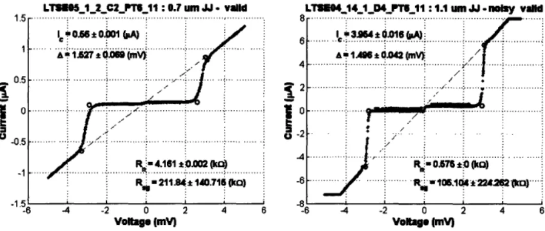
The algorithm also looks for a subgap regime around 0.75 mV times the number of junctions in the string. Once this region has been identified by similarities in slope, it averages slope to determine the subgap resistance. The averaging algorithm on the oscilloscope sometimes averages poorly, leaving half the points obviously on a higher line and half on a lower line. This would create a large problem in curve fitting if not corrected. The algorithm is designed to correct for this: the trace is defined as "noisy" if the points fall close to two different current values throughout the length of the sub gap regime. The current value with more points is considered correct and the other is shifted by an amount to equilibrate their means. This allows for more accurate fitting of the subgap. This is shown in figure (2 - 3).
The normal resistance is calculated by applying a least squares linear fitting algo-rithm to the normal regimes on both sides of the axis. Using both sides of the axis eliminates potential voltage offsets. The line is expected to go through the origin, as it is Ohm's law. With both quadrants present, it is safe to allow for a nonzero current intercept and justify it as an offset in current or voltage.
The program is less reliable for determining subgap resistance. This is because the data in this region does not always appear linear, and we do not have high resolution in this region. The individual subgap resistances for each side are calculated and averaged to provide this value. At this point, the subgap and normal resistances are compared. If they are similar, then the device is assumed to be resistive and a linear
LTIS_2_C2_PTI11: 0.7 um JJ valid LT_4_14__D4_PTL_1 :1.1 u JJ - mnoy valid 1.5 .. ... ... ... ... .. ... ..a...<... 8 ... ... ... 8 ... ... . ,: ...
1,5|
~
~
~
~
~ ~ ~ ~ ~ ~~~~~~~~~~~~~..
-... -
0...
...
0.5 .... .... ... ... ... . .... ...f
° - ° I,...
... ... ... ( _1 A.~h27±ODSS~~~mV) 0.001 . 00.A) 6 A~ . it .. ... Rn 0.676 . t 0 *0)0%,-211*140.716
g")
-6
... ..
1 2 -6 4 -2 0 2 4 6 4 -2 0 2 4 6 Votage (mV) Voltage (mV)Figure 2-3: Current voltages traces of two working junctions. These are direct output plots of the program. The second shows two artifacts of the data collection method. The presence of two distinct lines in the sub gap regime is because of the averaging, and the slight jump close to the negative knee is a mistake that comes from stopping data collection while the current is still sweeping back and forth.
fit is made to the whole set of data.
This is also the part of the routine where leaky and shunted junctions are identified. Examples of these two failure modes are shown in figure (A-3). Shunted junctions are identified because of the voltage jump at the origin. Leaky junctions are determined in two ways: either a similarity in subgap resistance to normal resistance but with overall resistance nonlinearity, or if the knees aren't steep enough.
To determine the characteristic voltages and currents of the junction, the program uses a series of linear fits. It estimates a slope for the knee and fits a line to the knee section. The intersection of this line and the normal line is at the knee voltage. The intersection of this line and the subgap line provides the subgap voltage. Averaging the positive and negative voltage measurements for each of these eliminates the offset. The algorithm assumes an error in measurement associated with scope resolution that is the distance in current between the closest points. The parameters extracted from each working trace are Vknee, Vsubgap, and Rn.
2.4 Analysis of Wafers
Analyzing individual traces for characteristics is very important but the most useful feedback cryogenic testing provides is from analyzing wafers as aggregates of junctions. Fabrication parameters are varied from wafer to wafer, so comparing wafer statistics is the most enlightening.
The two types of devices that are useful to analyze are resistors and Josephson junctions. While resistor analysis is full of subtly, it is not the focus of this thesis and so not much detail will be paid to it. In brief, resistor analysis is centered on the measured resistance and expected resistor width. Only one dimension is varied so a linear fit can be used to determine trends in width as well as resistivity. This analysis is based on the definition of resistance as R = where resistivity p and length I are constant for all devices. Area A is allowed to vary across devices. The equation to fit to is
W Wo I
w+
w = 1 (2.2)Rs R, Rn
with 1 being the length of the resistor, 100 um. Rn is the measured normal resistance, IV is the drawn size, Wo is the sum of all biases and Rs is the sheet resistance, a constant that only depends on the resistivity and height of the junction. A least-squares fit will give the best values of W0o and Rs. This analysis is done by die, and plotted by location on the wafer.
The analysis of Josephson junctions is covered in great depth in Chapter (3). The program automatically performs the analysis to determine parameters that are of use to fabrication. The parameters that are calculated for each die are the critical current density Jc and average process bias do. These results are plotted on displays of the wafers such as figure (A - 4).
The program also plots median characteristic values for each wafer. For Josephson junctions, it plots J and 60, and for resistors, it plots Rs and Wo. An example is
shown in figure (A - 5). A final summary that this program provides is of device type. This breaks down by size and wafer number how many of each failure mode there were. An example of this plot is shown in figure (A - 6).
Chapter 3
4
He Cryogenic Results
3.1 Energy Gap Determination
The most valuable asset of 4.2 K cryogenic testing at is the rapid feedback of otherwise unattainable information. Room-temperature testing can provide a value for normal resistance, but this resistance cannot be separated from the NbOx conductor on the outside of the junction. Likewise Jc can be measured at room temperature to within 10%, but information about the size of the junction cannot be determined unless it is cooled. Additionally, whether or not the junction functions correctly is also
unattainable at room temperature.
The junctions are drawn between 0.4 m and 1.1 pm in diameter, less than 5% of Aj which is 25 pm. With sizes this small, self-field effects do not significantly impact the critical current, as shown in section (1.5).
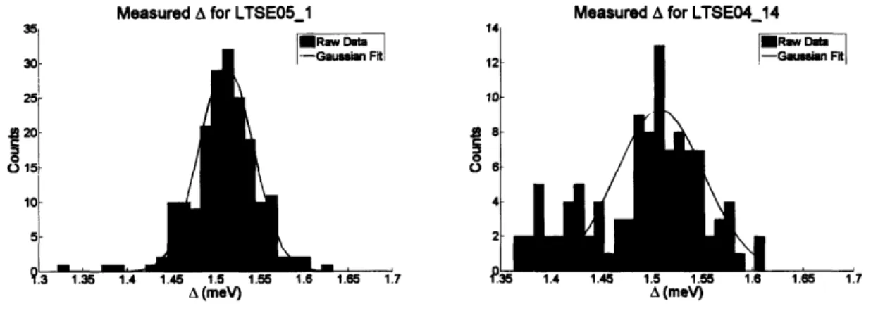
The first piece of data calculated is the superconducting energy gap. 2A/e is located between Vsubgap and Vknee as seen section (1.3). The average of these voltages is used to calculate the energy gap. Table (3.1) lists the mean values of A reported for each run. Histograms of calculated A are shown with the superimposed gaussians used for finding the mean and variance are shown in figure (3-1). All analysis follows standard error determination [27].
Experimental values of A confirm the assumption of treating this as a
Run Valid Junctions A meV
LTSE04_14 106 1.508 i 0.044
LTSE05_1 189 1.513 i 0.031
DSM205-19-8 96 1.511 ± 0.020
Table 3.1: Mean values of A for three runs. BCS predicted value for niobium is A(T=0) = 1.40 meV, from equation (1.10). This has been experimentally shown to be 1.55 meV, which is shown to be constant over 0.4 - 4.2 K [25].
Measured A for LTSE05_1
1__ _ I unEW n FL 3aussin F 30 25 o 15 a mev) 14 12 10
i8
6 4 2 1.65 1.7Measured A for LTSE0414
r1,~_.. n I
a mev)
Figure 3-1: Histograms of measured A from two of the three runs. The gaussian is only used for purposes of reporting a mean and variance in mean for A.
superconductor (NIS) junction is A/e, half the gap of an SIS junction [2]. The in-dividual junction's energy gap is used in further calculation. A shows no explicit dependance the on size of the junction. This is consistent with the prediction that A only depends on temperature and the material parameters. Variations in A can be
attributed to inhomogeneities in the materials.
The other parameter that is directly taken from the current-voltage trace is the normal resistance. Rn is the inverse of the slope in the normal regime. Together with equation (1.16), I, can be calculated.
3.2 Critical Current and Process Bias
The junctions are fabricated with an expected J¢ and expected diameter. The ex-pected Jc can vary with the wafer, as it is a parameter of fabrication. Any description
-Gausen Fit
1.65 1.7
of critical current density must include discussion about the geometry of the junction. The diameter of the junction is specified, but shifted by an unknown quantity 60, see equation (2.1). Additionally the barrier is not necessarily uniform.
Two steps are taken to simplify this analysis. The first step is the assumption is that the parameters of interest, 60 and J, do not vary on each chip. Additionally, a model must be adopted for the junction barrier. The simplest model neglects barrier pollution and assumes the barrier to be a flat disc. This is defined by equation (1.20). Bias is accommodated by separating the diameter into and 60, where is the sum of drawn size and optical. Values for 6
Nb0x have been observed, but since the bias is
constant with respect to junction diameter, we may let it vary and determine it for each chip. Therefore, the measured bias is a sum of the niobium oxidation bias and unknown biases which is known as the process bias.
To begin the analysis of bias and critical current density, Ic is written in a form that is quadratic in . There is no reason to deal with the quadratic though; the repeated roots imply that it is possible to linearize. The following line can be used to fit the data in this model,
4II
-Js6+
6
0.
(3.1)A least-squares method is used to fit the working junctions from each chip. The algorithm looks for points to throw out that are clearly outliers. It does this by recalculating the fit as is a given point had not been there. If removing a point changes the fit a great deal and would leave at least two points to fit, it removes the point from the fit. This allows the program to discount anomalies of the junction fitting algorithm. An example of a set of fitted data is shown in figure (A - 7).
There are several ways to organize the data to make viewing trends obvious. The most useful is to plot the desired data on top of the wafer so trends across the wafer can be seen. This is known as a wafer map, and an example can be seen in figure (A - 8). Another way of organizing the data is to show it as a comparison across wafers of the same run. An example of this is shown in figure (A - 5).
The results of this analysis reveals two important things: typical values of pa-rameters and trends across wafers and runs. Values from this analysis show high variance inside both wafers and runs. Variance between wafers in the same run is expected because processing is intentionally different. Variance inside single wafers can be attributed to processing inhomogeneities as well as inaccuracies associated with fitting lines to between 2 and 6 points.
Looking at the wafer maps, it becomes obvious that the assumption that these parameters change across wafers is valid. The effects of stresses and strains during deposition and processing (etching) make the junction parameters vary. Looking at figure (A - 8), the top left of the wafer has low process bias and low critical current while the bottom left has the opposite. In general, areas with low bias were observed
to have low critical current density.
Values for process bias range from enlargements less than 0.1 Am to reductions less than 0.6 m. The expected diameter pollution of niobium oxide falls into this range because it is between 0.1 and 0.2 m. Enlargements and reductions greater than 0.4 Am are not physical. The smallest junction is 0.43 Am, so a bias of that order would completely close off these junctions. Junctions of this size did yield on chips with calculated diameter reductions greater than 0.5 Am. Similarly, enlargements
would imply that there is no oxidation or that the junction has somehow expanded its effective area past what was drawn. Observation of oxidation makes these results nonphysical as well.
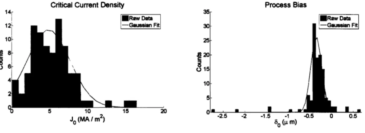
Similar conclusions may be drawn from J. The majority of wafers analyzed have a target J, of 5 ( 2 ). Critical currents were consistently calculated to be lower than
this target. This means that either the fitting is done poorly, or the resistivity is increased by a thicker barrier than anticipated. J is best evaluated on a wafer by wafer basis because of the varying target Jc. In the case of wafers with target J¢ of 5
( ), a histogram and gaussian fit current by die is shown in figure (3 - 2). Typical
Variable Typical Value
J
4.88 2.81
(A )0 -0.35 ± 0.12 (m)
Table 3.2: Typical values of fitting parameters from the linear model. For finding J, only junctions with expected J of 5 A are used. For finding 60 all junctions are
/m2
used.
Critical Current Density Process Bias
14r o a Cis Jo (MA/m2) = , 15 20
Figure 3-2: (Left) Histogram and Gaussian fit of fitted die J from die of wafers with expected J of 5 A. The gaussian is used for mean and error determination with
results listed in table (3.2). (Right) Histogram and gaussian fit of the process bias of all die analyzed. The gaussian is used for mean and error determination with results in table (3.2).
3.3 Barrier Pollution Analysis
Knowing that fabrication never produces ideal junctions, it is natural to question the validity of such an ideal barrier model. One way inaccuracies would manifest would be reoccurring nonlinearities in the data. A way to check for this is to analyze the residuals of the linear fit. If certain diameters consistently deviate in the same way, it indicates the necessity of a new model. This could also mean that new values are needed for expected biases. Fitting residuals from run LTSE05_1 are shown in figure (A - 9). The residuals plotted on this graph exhibit a clear size dependance, indicating a systematic problem with analysis.
Another check of the model is executed by relaxing the linear assumption and
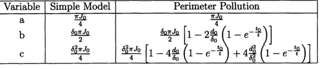
Table 3.3: Table of fit values for the quadratic fit y = ax2 + bx + c of Ic(6).
quadratic would be zero, indicating repeated roots. Before performing this check, it is useful to speculate what the determinant should be in an alternate model.
A natural model to adopt is one that treats perimeter pollution effects in a simple way. The model in equation (1.21) and figure (1 - 2) treats this effect. We must again add the bias effect, so 6 becomes 6 + 60. Because the barrier is only a few monolayers in thickness, it is likely that the pollution would also only be a few monolayers in thickness. If the barrier were much thicker, that section of barrier would probably be too thick to contribute significantly to the critical current. This model does assume, however, that the pollution is uniform thickness and has width and height that is independent of size. For this reason a model like this will merely serve to give a bound for this effect rather than produce actual numbers. While the quadratic fit may be used in either model, the parameters represent different values. The parameters of the y = ax2 + bx + c fit are shown in table (3.3) in terms of the constants of the models.
The perimeter pollution model changes the linear and constant term of the fit. A way to compare the models quantitatively is by looking at b2- 4ac. For the simple model this is 0 because the roots are repeated. For the pollution model this is not zero. Dividing by a2 reduces it to parameters of the pollution,
b2- 4ac 2-(
a2 =-- 16 d 1-e t e t. (3.2)
Because fitting to a parabola requires at least 3 points, the data available to this analysis is very small. Also, in sets with small numbers of data points, bad points can throw off the fit a great deal. A histogram of this modified determinant shows
Variable Simple Model Perimeter Pollution
a 4
b (rJ o0-Jo ° rJp -d -e
c
Jo [6Jo
1-4I-e-t
+
4
1
-1-eet
77 of the 81 points clustered together at the origin and the last 4 are discarded as outliers. A gaussian fit to the histogram is shown in figure (A - 10). The result does not fit either model perfectly. There is a great deal of deviation from the origin, unlike the simple model predicts, and while the pollution model predicts a negative mean, the determinant is centered around the origin.
This data may be used to predict a maximum value for the perimeter pollution depth, however. Assuming to is positive, meaning increased thickness due to oxida-tion, then (1 -e-t e varies between 0 and -0.25. To establish a maximum we must minimize to/t. A natural lower limit is 1/5, which would represent a single monolayer contamination in a barrier five monolayers thick. This would leave the modified determinant approximately equal to 2 d2. An upper bound is established by taking the variance of the mean to be a typical value for the modified determinant. The approximate maximum is 60 nm, which when doubled to effect the diameter is of order 0.1 ,um. This implies that while the entire junction is shrunk by 50- 100 nm from oxidation, additional oxidation effecting barrier thickness is limited to about 60 nm of penetration.
Cryogenic testing of Josephson junctions is very important for providing feed-back for fabrication. Values for normal resistance and the superconducting energy may be extracted from the current-voltage trace of the junction, both of which are unattainable at room temperature. The critical current may then be calculated from these results. When this value is compared across many junctions on the same chip, values for critical current density and process bias may be calculated. These values are shown to vary across each wafer. Adopting a model of perimeter pollution allows for the determination of an upper limit of barrier pollution, which is shown to be approximately 0.06 tim. Summary values for all variables attained from cryogenic testing are shown in table (3.4).
Table 3.4: Summary of values from analysis. Some outliers were discounted in the range determinations, but only those that were clearly mistakes of fitting. These statistics encompass all 391 junctions used in analysis.
Variable Range Average
RN 0.10 - 863 kQ 13.88 kQ Vknee 2.85 - 4.49 mV 3.12 mV Vsubgap 2.43 - 3.11 mV 2.92 mV A 1.33 - 1.63 meV 1.51 meV Jcl 0.10 - 181 () 4.88 ( m2) 60 -0.80 - 0.67