Analog to Digital Converters for CMOS Imagers
by
Susan Dacy
Submitted to the Department of Electrical Engineering and
Computer Science
in partial fulfillment of the requirements for the degree of
Master of Engineering
at the
MASSACHUSETTS INSTITUTE OF TECHNOLOGY
June 1998
@
Susan Dacy, MCMXCVIII. All rights reserved.
The author hereby grants to MIT permission to reproduce and
distribute publicly paper and electronic copies of this thesis
document in whole or in part, and to grant others the right to do so.
Author... . ... .- ...--
Department of Electrical Engineerin' and Computer Science
May 8, 1998
Certified by...
...
Charles Sodini
Professor of Electrical Engineering
Thesis Supervisor
Certified by...
...
Marc Loinaz
Member of Technical Staf,-Bll Laborato
,Lucent Technologies
/
-•
-- lýheIs
Supervisor
MA SACiSS INST'TU
JUL 14 1998
Arthur C. Smith
I airman, Department Committee on Graduate Students
Analog to Digital Converters for CMOS Imagers
by
Susan Dacy
Submitted to the Department of Electrical Engineering and Computer Science on May 8, 1998, in partial fulfillment of the
requirements for the degree of Master of Engineering
Abstract
A/D converters for single chip CMOS imagers have often been designed using the column-parallel approach, employing a slow A/D converter for each column of the sensor array. This thesis investigates a serial approach utilizing a single fast A/D converter to process all of the imager pixels. If power scales linearly with frequency in a given A/D architecture, power dissipation for the two approaches should be com-parable. However, the serial approach should occupy less area since only the cost of
one A/D converter is incurred. A figure of merit ( p powersarea) is introduced to ver-ify this theory by comparing previously reported A/D approaches after appropriate technology, speed, and supply scaling.
Camera system specifications require a single serial A/D converter to have 10b resolu-tion at a 3MHz sampling rate for a CIF (352x288) imager array running at 30 frame
Area minimization, power minimization, and the ability to build the A/D in a stan-dard CMOS process are extremely important for consumer product applications. A single slope A/D architecture with a subnanosecond time digitizer shows promise for optimizing figure of merit over pipelined and folding interpolating approaches. This work focuses on the design issues of the 3MHz single-slope based A/D converter. Architectures appropriate for extending this A/D converter to 12MHz for four times CIF image arrays (704x576) are discussed.
The 3MHz converter was designed, simulated, and laid out in a 0.35um CMOS tech-nology. At 3.3V supply, 25°C and nominal process conditions, the converter dissipates 29 mW while occupying 0.3 mm2. A 12MHz trislope extension of this converter is
estimated to dissipate 37 mW in 0.4 mm2 Thesis Supervisor: Charles Sodini
Title: Professor of Electrical Engineering Thesis Supervisor: Marc Loinaz
Acknowledgments
This research was completed at Bell Labs Innovations for Lucent Technologies in Holmdel, NJ under the MIT VI-A program. Many people in the DSP & VLSI Research Department deserve thanks for their friendship, advice, and technical assis-tance. I would like to thank Patrik Larsson for helping with the PLL and reading this thesis, Chris Nichol for help with the low-power digital circuits, Venu Gopinathan, Turi Aytur, Dan McMahill, Steve Decker, and Harry Lee for attending my design re-views and brainstorming with me, and Bryan Ackland for reading drafts of my thesis proposal and thesis. Thanks also to Dave Inglis, Kim Dugo, and Jay O'Neill for their support.
I'd like to give a special thanks to my Thesis Supervisor, Marc Loinaz. Marc provided the inspiration for this research. He has taught me to be an independent researcher, to give clear presentations, and to justify my design decisions. Thanks are also due to Charlie Sodini for his support and encouragement during my internship at Bell Labs.
My gratitude goes to the DOD/NDSEG Fellowship Program and Lucent Tech-nologies for funding this research.
Finally, I'd like to thank my family for their support during my education at MIT and Bell Labs.
Contents
1 Introduction
2 Analog to Digital Converter Performance Requirements 2.1 Analog Signal Chain of CMOS Imager . . . . 2.2 Analog to Digital Converter Specifications . . . . 2.2.1 Performance Metrics . . . . 2.2.2 Analog to Digital Converter Requirements . . . . .
3 Number of Converters
3.1 Column Parallel Approach ... 3.2 Semi-Column Parallel Approach . . 3.3 Serial Approach and Architectures .
3.3.1 Pipeline ...
3.3.2 Folding Interpolating .... 3.3.3 Single Slope ... 4 Single Slope Architecture
4.1 Traditional Single Slope ...
4.2 New Single Slope with Sub-nanosecond Time Digitizer . . . . 4.3 C alibration . . . .
5 Design of a 10b, 3 MS/s Single Slope A/D
5.1 Introduction . . . . 5.2 Tim e D igitizer . . . . 11 11 15 15 19 23 . . . . 24 . . . . . 25 . . . . . 26 . . . . 27 . . . . 28 . . . . 28 29 29 31 33 34 34 35
5.3 5.4 5.5 5.6 5.7 5.2.1 Overall Architecture . . . . 5.2.2 Ring Oscillator and Phase Locked 5.2.3 Latches ...
5.2.4 Coarse Counter . . . . Track & Hold ...
Ramp Generator ... Comparator ... Calibration ... Layout .. ... . . . .... 6 Extension of Design to 12MHz 6.1 Increasing LSB Resolution ...
6.1.1 Faster Ring Oscillator . .
6.1.2 Interpolation Between Edges 6.2 Subranging ...
6.2.1 Tri-Slope Converter ... 6.2.2 Integrated 2b Flash . . . . .
7 Simulation Results and Conclusions
Loop.
° o. . . ° ° ° ° .
List of Figures
Active Pixel Sensor . . . . Single Chip Camera Architecture . . . . Spectral Response of Photogate Sensor . . . Ideal A/D transfer characteristic . . . . Poor DNL Example: Missing Output Code . Transfer curve with large INL ...
Quantization Error ... Noise of Imager Pixels ...
Blank Pixels Between Lines and Frames . .
3-1 Typical Pipelined Converter . . . . 3-2 Folding Architecture ...
4-1 A 10b, 3MHz Traditional Single Slope Architecture . . . 4-2 New Single Slope Architecture with Subnanosecond Time 4-3 Linear Tradeoff Between Resolution and Speed . . . . 4-4 Single Slope Endpoint Calibration . . . .
Digitizer
Single ended representation of Single Slope Architecture Single ended representation of Time Digitizer . . . .
Phase Locked Loop Block Diagram . . . . Ring Oscillator Stage ... ...
B uffer . . . . fully-differential to single ended converter . . . . 2-1 2-2 2-3 2-4 2-5 2-6 2-7 2-8 2-9 . . . . . 12 . . . . 13 . . . . 14 . . . . 16 . . . . 17 . . . . 17 . . . . 18 . . . . 2 1 . . . . . 22 5-1 5-2 5-3 5-4 5-5 5-6 41 41
5-7 5-8 5-9 5-10 5-11 5-12 5-13 5-14 5-15 5-16 Coarse Counter
Interleaved Track & Hold . . . . Folded Cascode Amplifier . . . . Ramp Generator Model . . . .
Ramp Model ...
Ramp Voltage versus Time . . . . INL versus Time(Trigger Point or Vin) . . Ramp Implementation . . . . Comparator ...
Small Signal Model for determining output A/D Calibration loop . . . . A/D Layout ...
Ring Oscillator Routing . ... Weighted Summer used as an Interpolator Architecture using Interpolators . . . . Trislope Converter . . . . Coarse 2b Flash ...
edge
° . ,
Single ended divide by 2 . . . . Divide by 17 . ... . . . ...
Phase Detector ...
Dead zone in phase transfer characteristic . . Charge Pump ...
Loop Filter ... . ... .. ... ... Phase Locked Loop Parameter Block Diagram Block Diagram from Output of Buffers . . . Fully-Differential, Master Slave Latch . . . . .
5-17 5-18 5-19 5-20 5-21 5-22 5-23 5-24 5-25 5-26 5-27 5-28 6-1 6-2 6-3 6-4 rate ... : : : : :
List of Tables
2.1 A/D Specifications ... 19
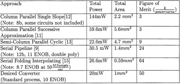
3.1 Scaled Comparison of Previously Reported A/D Approaches .... . 26
5.1 PLL Loop Crossover and Stability . ... . 48
5.2 Chip Area Breakdown ... 68
7.1 Power Consumption ... 77
7.2 Summary of Sources of A/D Nonlinearity . ... 77
Chapter 1
Introduction
CMOS technology is used for most microprocessors and ASICs, and is backed by an enormous worldwide research and development effort. Device feature sizes are decreasing by about a factor of two every five years. The CMOS Camera Project at Lucent Technologies explores the use of this booming CMOS technology for imaging applications. Building an imager in CMOS technology allows processing circuits to be integrated on the same monolithic chip. This system integration will allow CMOS cameras to provide low-cost, low-power solutions for applications such as video conferencing, document imaging, and security/surveillance [1].
Power minimization, area minimization, and the ability to build the imager in a standard CMOS digital process are extremely important for consumer product applications. High localized power dissipation can degrade the performance of the imager sensor and reduce the benefits of on chip Analog to Digital (A/D) conversion
[2]. Area minimization is essential for reducing fabrication costs. Building the imager in a standard, digital CMOS process is also important for cost reduction and for initiating widespread use of CMOS imagers. This thesis focuses on the design of an A/D converter in a standard, digital CMOS process for a 352x288 imager that minimizes power and area. Avenues for extending this design to a larger (704x576) imager array are discussed.
The thesis is organized as follows. In Chapter 2, the analog signal chain through the imager is described. The operation of CMOS pixels, readout circuits,
pro-grammable gain amplifier (PGA), analog to digital converter, control logic, and the overall single chip CMOS camera are explained. Performance specifications for the A/D converter are derived from the overall camera requirements.
Chapter 3 addresses the number of A/D converters needed in an imager to min-imize power and area. Column-parallel, semi-column parallel, and serial approaches are compared. The serial approach is selected for its potential to minimize area. Ar-chitectures appropriate for the serial approach are described. The new single slope architecture is investigated for its potential to minimize the power-area figure of merit over pipelined and folding interpolating approaches.
Single slope approaches are explained in Chapter 4. The new single slope architec-ture with a subnanosecond time digitizer is compared with a traditional single slope design. The overall architecture and calibration scheme for this new single slope A/D are detailed.
Chapter 5 details the analog circuit design involved in implementing the new single slope architecture described in Chapter 4. The major analog blocks include the time digitizer, track and hold, ramp generator, and comparator. Design tradeoffs are justified in terms of their minimization of power and area. The digital calibration loop algorithm and implementation is also discussed. Layout of the chip is explained. Issues encountered include optimizing layout to minimize mismatch, area, and noise coupling.
Chapter 7 elucidates an extension of the 3MHz design to 12MHz. Architectures based on increasing LSB resolution and subranging are discussed. Power and area numbers for the 12MHz design are predicted from the achieved 3MHz power and area
numbers.
Chapter 8 reports simulation results for the 3MHz A/D. The power-area figure of merit for the 12MHz extension is compared to the current imager A/D design, column parallel and semi-column parallel approaches, and previously reported pipeline and folding interpolating designs.
Chapter 2
Analog to Digital Converter
Performance Requirements
The A/D performance specifications are derived from the overall camera requirements. These specifications aid the selection of an A/D architecture. Section 2.1 describes the operation of a CMOS photogate pixel. The analog signal chain is then traced from the pixel through the PGA and A/D to the control logic and calibration. The operation of the overall single chip CMOS imager is detailed. Section 2.2 derives the A/D specifications from the desired imager system performance.
2.1
Analog Signal Chain of CMOS Imager
Active pixel image sensors (APS's) are the origin of the analog signal in the CMOS imager. APS technology is a low power, low cost, easily integrable alternative to CCD technology. Active pixel sensors can easily be built in CMOS technology with analog processing circuits, and digital timing and control electronics. The main disadvantage of APS technology compared to CCDs is process dependent leakage current and low quantum efficiency [3].
A pixel schematic with readout circuits is shown in Figure 2-1. Charge is inte-grated under the photogate for a fixed period of time (integration time). During integration, the polysilicon Photogate is held at Vdd and photo-generated carriers are
Vb2
·-1C
Phe
To PGA
Figure 2-1: Active Pixel Sensor
collected beneath the gate oxide. Vbias is held at around 1.OV to isolate the collected charge from the Signal Node when the photogate voltage is high. During readout, the
Signal Node is reset by pulsing Reset high and turning on Ml. The reset level of the
signal node is copied by the source follower M3-M5 onto the gate capacitance Cr by pulsing SHR to Vdd. Photogate is then driven to ground, turning on M2 and transfer-ing the collected charge to the Signal Node. This charge displaces the voltage on the
Signal Node by an amount that depends on the incident light intensity. The charge
is then sampled on the gate capacitance Cs by pulsing SHS. Column Source followers M11-M16 drive the double-sampled signal into the fully differential, switched capaci-tor PGA. On one clock phase of the PGA, these signal and reset values are sampled. On the other clock phase, crowbar (CB) is pulsed and the offset difference between the column source followers is sampled and subtracted. This two-level correlated double sampling suppresses column offsets, pixel k noise associated with the reset operation, 1/f noise, and fixed pattern noise due to threshold voltage variations [4].
The pixel consisting of the photogate and M1-M4 of Figure 2-1 is repeated in a 352x288 array as in Figure 2-2. The two-level correlated double sampling circuit consisting of M5-M16 in Figure 1 is repeated at the end of each column in Figure 2-2. Each pixel in the array has a color filter that allows either red, green, or blue light to pass through. The signal and reset voltages of these pixels are fed as a fully
It
rrr%356x288 imager
row decoders pixel
row address column address
output circuits & column decoders
Signal Reset DSP
control
PGA host interface
fully color interpolation
differential color correction
exposure control
Figure 2-2: Single Chip Camera Architecture differential signal into the Programmable Gain Amplifier (PGA).
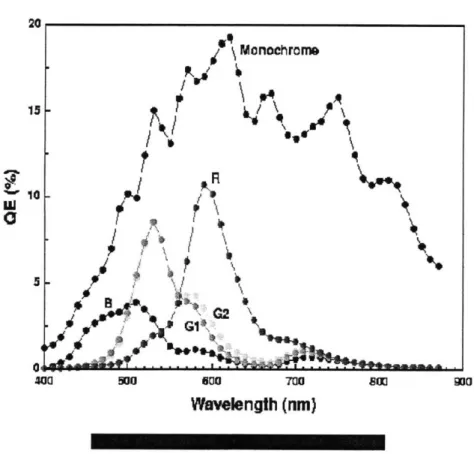
The PGA provides variable gain to individual pixels. Programmable gain allows for correction of silicon's varying spectral response as shown in Figure 2-3. Specifically, the photogate sensor has a poor blue spectral response. When a blue pixel is read out, the PGA can amplify that pixel relative to the red and green pixels in order to achieve white balance. In low light conditions, the PGA can amplify all the pixels. This form of automatic gain control helps relax the resolution needed by the subsequent analog to digital converter.
The PGA design was investigated in Summer 1996. The PGA had a programmable gain from 1-16 and a 3db bandwidth of 60MHz with a gain of 16 under a 2pF load.
The fully differential output signal had a 2V range with a 3.3V supply. The PGA consisted of a fully differential, high gain-bandwidth op amp in a switched capacitor integrator configuration. Two pipelined PGA stages, each with a programmable gain from 1-4 were used to meet the specifications [5].
WI
'U
400 5IO 600 700 80B
Wavelength
(nm)
(A/D). The digital output of the A/D is then processed by the Digital Signal Processor (DSP). The DSP is responsible for color interpolation and color correction of this digital output. The R, G, and B values for a single pixel are interpolated from the surrounding pixels by interpolating from a 3x3 neighborhood surrounding each pixel.
Color correction involves a linear 3x3 matrix transformation that minimizes mean colorimetric error [6].
2.2
Analog to Digital Converter Specifications
The A/D in Figure 2-2 converts the fully differential PGA output into digital codes that can be processed by the DSP. Performance metrics for the A/D are defined in Section 2.2.1. Specifications for the A/D performance are derived from the overall imager system requirements in Section 2.2.2.
2.2.1
Performance Metrics
Several parameters are used to measure the performance of an A/D. The param-eters relevant to this A/D design are discussed below.
Conversion Rate
Conversion rate is the number of digital samples an A/D can convert in a given amount of time, measured in MSanles. For Nyquist rate A/Ds, the input signal frequency is limited to half of the conversion rate. In CMOS imager applications, the analog input voltage is held constant by the PGA. The conversion rate (f,) in the imager application is governed by the size of the imager (r*s pixels), frame rate (f) and the number of A/D converters used (N):
fe
= (2.1)The
tradeoff
between
f
and
N
be discussed further in Chapter 3.N
will
Differential Nonlinearity (DNL)
For an ideal A/D, the digital output codes as a function of the analog input voltage are shown in Figure 2-4.
Dout Di+1 Di Vin Vi Vi+l Vlsb
Figure 2-4: Ideal A/D transfer characteristic
In an ideal A/D, the analog input voltage change corresponding to two adjacent output codes is equal to the voltage Vsb. Vlsb is the voltage corresponding to one Least
Significant Bit (LSB). One LSB is - where VFs is the full scale input voltage and n is the number of bits of the converter. A/D non-idealities can cause the spacing between adjacent digital output codes to be greater than or less than one LSB. Differential Nonlinearity (DNL) is a measure of this error and is defined as [7]
DNL[i] - i+ 1 (2.2)
VLSB
where i is the index at which DNL is being measured. This measurement is defined in units of LSB's.
An extreme example is shown in Figure 2-5. The digital output code Di never appears at the output. In this case, the DNL=-1 for the code Di. From equation 2.2 a DNL of -1 is the worst case negative DNL and a code is missing. On the other end of the spectrum, a code can be very wide and have a positive DNL greater than 1. DNL is a measure of the error in the resolution of the A/D.
Integral Nonlinearity (INL)
Integral Nonlinearity (INL) measures the absolute accuracy of the A/D. INL in LSBs is the difference between the actual A/D transfer curve and the ideal A/D
Dout Di+2 Di+l Di Vin Vi=Vi+l DNL- 1
Figure 2-5: Poor DNL Example: Missing Output Code
transfer curve as shown in Figure 2-6. INL is defined after correction for gain and offset error. In the example of Figure 2-6, the DNL is small, but integrates to give a large INL in the middle of the transfer curve [7].
Dout
Vin
Figure 2-6: Transfer curve with large INL
Signal-to-Noise Ratio and Effective Number of Bits (ENOB)
Quantization error is defined as the difference between the original input and the digitized output converted back to an analog signal using an ideal D/A. Quantization Error for an ideal A/D transfer curve is shown in Figure 2-7. The quantization error decreases as the resolution of the converter increases. Quantization error can be modeled as an additive noise source appearing at the output [7].
Assuming the quantization error is uniformly distributed and independent of the analog input, the quantization noise power can be expressed as the mean square of the quantization error in Figure 2-7 [7]
Lngio Outpu Vlsb 5Vlsb 2 2 Quantization Error Analog Input
Figure 2-7: Quantization Error
IV
f 211Sb V2dV 1
Vnoise,rms = b sb (2.3)
A sinusoidal analog input with a peak-to-peak voltage of VFS = 2" V* Isb (where n is the number of bits) has an RMS value:
1
VFSRMS = 2 Vlsb (2.4)
2V2
Thus an ideal n-bit A/D with a sine wave input has an SNR:
SNRFs[dB] = 20 loglo VFsRMs = 6n + 1.76 (2.5)
Vnoise,rms
For example, an ideal 10-bit A/D has a peak SNR of 61.76 dB. While SNR is a measure of the noise level of an A/D relative to its peak input signal, Signal to Noise plus Distortion Ratio (SNDR) is a measure of the noise plus harmonic distortion relative to the input. This distortion is a result of nonlinearity (INL) of the A/D. Effective Number of Bits (ENOB) is computed by measuring the SNDR and using equation 2.5:
SNDR[dB] - 1.76
ENOB =(2.6)
6
A/D. ENOB can be measured as a function of the sample rate and bandwidth of the incoming signal, whereas INL & DNL are "DC" parameters.
2.2.2
Analog to Digital Converter Requirements
The A/D specifications are listed in order of importance in Table 2.1. These specifications are justified in terms of the overall camera system requirements.
Table 2.1: A/D Specifications Resolution 10 bits
Conversion Rate 356 * 288 * 30•' -= 3Msampes 1 2 Msamples
DNL < 0.5LSB
INL Not critical - < 5LSB
Area < 1mm2
Power < 20 mW
ENOB > 8b
Supply 3.3 Volts
Technology 0.35um, no linear capacitors or resistors Calibration flexible- several lines of blanking intervals Input fully differential
Temperature 00-700C
Supply variation 3.3V ± 10 % Vincommonmode 1.5V
Vindifferential 1V
The resolution needed by the A/D is reduced by the gain control function of the PGA. In medical and scientific imaging applications, 12b resolution is often needed with a CCD imager. In consumer electronics, 8b or 10b resolution is commonly in use. Figure 2-8 shows the output signal level relative to the photon shot noise and dark current shot noise for a CMOS photogate imager [3]. This shows that the imager signal to noise ratio is only about 50dB, or 8 bits. Thus the A/D should achieve at least 8 effective bits (ENOB) so that camera performance is limited by the imager and not the A/D. An A/D resolution of 10 bits is needed for digital post processing (about 2 bits of resolution are thrown away in digital post processing). Additionally, as the signal to noise ratio of the photogate pixel improves, higher resolution converters will
be needed. For CCD applications where the imager signal to noise ratio is higher, a higher resolution converter will be needed.
For the 356x288 imager running at a CIF standard frame rate of 30 f, mes
conversion rate of 3 Msamples second is needed in a single A/D from Equation 2.1. Also of interest is extending this design to a four times CIF image array (704x576), requiring
a conversion rate of 12 Msamplessecond
The A/D does not require good integral nonlinearity (INL), but does require good differential nonlinearity (DNL) - less than half an LSB. This is because the human eye is logarithmically sensitive to light intensity. The eye is sensitive to the difference in pixel intensities, not the absolute linearity of the intensity difference [8].
Area and power minimization are the main challenges in this A/D design. Area consumption will be minimized, with a target of 1mm2 in 0.35um CMOS. The area of the A/D is part of the cost of fabrication. Cost reduction is essential for the consumer products market. The current single chip imager in [6] has a total die size of 100mm2. This includes the imager, readout circuits, PGA, A/D, and digital color processing. The target lmm2 is about 1% of this total chip area, and a factor of three reduction in area over the 3.6mm2 A/D reported in [6]. Power dissipation will also be minimized, and should not exceed 20 mW. The power dissipation for the total single chip imager reported in [6] is 188mW. The target of 20mW is 20% of this total power and a factor of two reduction in A/D power over the converter in [6]. The analog circuits on the imager chip will operate with high quiescent power dissipation compared to the dynamic power dissipation of the digital circuits. Thus, as technology and supply are scaled, an increasing fraction of the total power of the imager chip will be dissipated by the analog circuits. Power minimization techniques are essential for the design of a scalable imager A/D [9].
The technology available for fabrication of this A/D is 0.35um CMOS with a 3.3 Volt supply. Design challenges in this technology include using a standard digital process. This means that there is no high-resistance poly available for making large resistors in a reasonable area. The sheet resistance of the polysilicon in this digital process is about 30 squareu , indicating that large resistors will consume a lot of area.
. 1 _ ._. !.F i ill ~Z~i~t . I -- w--i~---- - ' .:...i. i i. ItD~lf~ 15~ -~--~-U-~J~C~T~ i 1 ir~c~~ -~-~-~-~ · i ' i ~3 -- ·I--I, ~- ---*-c -- · -*- -~-*-pl "" L-C I u ~ I- -- ·-i i; I 10- 1 Sh ·--· -- · ·- --- · ""' ic, i-~II. i c-i pow 10o
Illuminance
(lux)
le I" ~ I I, _L I -e1. ~ ~cl +- I--lr I -L. L -5 L 101 -t-I,. f I,T
-e
.~i~ i I i -* I -5· -- I---L ·-e -+ t -r-i i 102Figure 2-8: Noise of Imager Pixels
.I~. -r I, i-- cc-;--· rr 10IU" loo 4-1 '3 O 10-2 S102 I n-4 .narl* eI ~I w RI&uI% -2 10 I I _ ·__·· _~_·I III~-II-~·IC·--·-·-L-li·--- IIII~-II-~·IC·--·-·-L-li·---III~-II-~·IC·--·-·-L-li·----r-·-·III~-II-~·IC·--·-·-L-li·---·IIII~-II-~·IC·--·-·-L-li·----·-CII I : ~C_ " i i --- ct--- (-·--CI-L--- ~(-·--CI-L---t- ~---t- ~i--i-i / I 1 ~---~ -- · · ^--··--t---LI ? - · ··~ I 1 ~c-~T~c 1Rt Isr c I" ---7C -~'^- II" ---~· -- - -- ·- -,-·---- - -- ----+--I -i Illlill
~---;f-i
II~-
~~~ .~~.~
'"
~I
--
r--· -r _L d ~ -*I T--*I -e ;Z~ -L I" -r. -e I ---- , --- ·. ---, - --- --· _1 .I~i-.. ---- -t--L. ---·t ---- r- -- I-ii cl -- ·-i m -~---,-I__
" " ' m ' i ' i ' I_ m -, j L356 pixels 35 pixels 356 pixels 3500 pixels Input to A/D
HSYNC *ee
VSYNC
*--Figure 2-9: Blank Pixels Between Lines and Frames
There is also no thin dielectric available for making large capacitors in a small area. Standard Poly/M1/M2 have a capacitance of around 6 * 10-2 -, so large capacitors will also consume a large amount of area. Ideally, the A/D will be an all-MOS design utilizing only small resistors and small capacitors. However, as capacitors and resistors become smaller, they are more sensitive to mismatches.
The input signal for the A/D is shown in Figure 2-9 (assuming one A/D is used). There are 35 "blank" pixel times between each line of 356 pixels. Blanking intervals exist for line and frame synchronization in video systems. For a 3MHz clock, this allows about 12usec for calibration. Between frames, there are 10 blank lines (3500 pixels), allowing lmsec. This dead time gives flexibility in the calibration scheme that may allow extra design opportunities for power and area minimization.
Since the A/D will be embedded on the same chip with the imager, the A/D should not produce too much substrate or supply bounce. This bounce is especially critical during pixel readout. By minimizing full scale voltage switching at high frequencies, this bounce should be reduced. It is even more important that the A/D converter be
insensitive to switching noise caused by digital control and processing circuits on the chip.
Circuits that are not part of the pixel array, including the A/D, will be covered by a light shield. This avoids high leakage currents and degradation of signals caused by photo-generated carriers.
Chapter 3
Number of Converters
The A/D architecture chosen for imaging applications is highly dependent on the number of converters, since the number of converters determines the speed of A/D operation. The optimal A/D solution for consumer products applications minimizes the total power and area of all the converters needed to process an image.
power/area figure of merit is defined as 1 . Power and area are weighted
equally in this formula, so designs are equivalent even if they dissipate twice the power as long as they occupy half the area. This formula assumes that all designs are 10b and that they have been scaled for 0.35um technology, 3.3V, and the appropriate conversion rate. The optimal A/D solution has the largest figure of merit. The extension of this design to a four times CIF imager array size (704x576) is ultimately important. Thus, the comparisons in this chapter are done for a 704x576 imager operating at 30 fsm, giving a conversion rate of 12MHz.
Section 3.1 describes the column parallel approach and gives some previously reported data. Section 3.2 details the semi-column parallel approach. Section 3.3 describes the serial approach. Previously reported power and area numbers and figure of merits are compared for all approaches. These numbers indicate that the serial approach should result in maximum power/area figure of merit. Architectures appropriate for the serial approach are described. The new single slope architecture is chosen for its potential to minimize power and area relative to folding interpolating and pipeline approaches.
3.1
Column Parallel Approach
The column parallel approach involves building an A/D at the bottom of each column. This A/D processes all the pixels in that column. The number of A/D's needed is now equal to the number of columns - 704 in this case. The speed of the converter is smaller than would be necessary with a single A/D, down by a factor
of 704 to 17 ksamples second " However, a PGA will be needed on every column, thereby
decreasing the bandwidth but increasing the overall area costs of the PGA. If no PGA is used, the resolution of the converter will need to be increased. Although some reported designs have used 10 bits without a PGA, the use of color filters degrade the sensor signal by a factor of around 10. Thus, about 12 bits of resolution will be needed for operation down to 1 lux [10]. Each A/D in the column-parallel approach needs to achieve 12 bit resolution, less than 20mrW*2 = 56.8uW of power
dissipation and minimal area consumption at 1 7 ksames second The factor of two in the
power spec is because no PGA is needed. The 20mW of power budgeted for the PGA can therefore be added to the 20mW already budgeted for the A/D.
A column parallel approach utilizing a successive approximation converter was taken in [11]. A slow 10b successive approximation converter was built in the pixel pitch width at the end of each column. Each A/D occupied 0.094 mm2 in 1.2um technology. Scaling for 0.35um technology and multiplying by 704 gives a total area of 5.6 mm2. Scaling the quoted single A/D power consumption of 8.6uW from 5V to
3.3V, 333Hz to 17kHz, 1.2um to 0.35um, and multiplying by 704 gave the total power number of 59.6mW. Scaling of power with conversion rate, technology, and supply was done linearly.
A column parallel approach was also taken in [12]. Slow 8-b standard single slope converters were built at the end of each column of the imager. Each A/D occupied 0.1 mm2 in 2um technology. Note that this area does not include the counter, ramp generator or any calibration circuitry, which were built off chip. Scaling for 0.35um and multiplying by 704 columns gave a total best case area of 2.2 mm2. The 125uW
for the ramp generator and counter are not given). Scaling from 5V to 3.3V, 1.2 ksamples second to 17 ksamples second 2um to 0.35um, and multiplying by 704 gave a total power
consumption of 144mW. Scaling of power for supply, conversion rate, and technology were done linearly.
Both of these column parallel approaches were used for a small array size at low conversion frequencies. When appropriately scaled for a large array size at high conversion frequencies, the total power and area consumption are large as summarized in Table 3.1. These two converter power/area figure of merits were the highest of those found in the literature. These A/Ds were probably not aggressively optimized for power and area, since their overall power and area were small in absolute terms for small array sizes operating at low conversion frequencies.
Designing column parallel A/Ds has the additional layout challenge of fitting the A/D in a pixel pitch width, which in this application is a factor of 2 smaller than in [11] or [12]. Column parallel A/Ds also have the potential problem of mismatches between A/Ds in different columns causing fixed pattern noise. This issue was not addressed in [11] or [12].
3.2
Semi-Column Parallel Approach
Another option is a semi-column parallel approach in which one A/D is used for every x columns [2]. This decreases the conversion rate over the serial approach by a factor of 704 However, it increases the area by a factor of 704
A semi-column parallel approach was used in [13]. A 10-b cyclic A/D converter was designed for every 2 columns of the imager. Each A/D occupied 0.07mm2 and
dissipated 100uW of power. Scaling for 0.35um technology, the total area of 74 such converters is 4.7 mm2. The power dissipation is 22.6mW after scaling from 15.3
kSamples to 34 kSamples 5V to 3.3V, and 0.8um to 0.35um. Scaling for conversion rate,
second second
power supply, and technology was done linearly. The power/area figure of merit is better than the column parallel approach, but still smaller than the desired figure of merit as shown in Table 3.1. The semi-column parallel approach still has the pixel
Table 3.1: Scaled Comparison of Previously Reported A/D Approaches
Approach Total Total Figure of
Power Area Merit ( kpowe-*area) Column Parallel Single Slope[12] 144mW 2.2 mm2 3
(Note: 8b, some circuits not included)
Column Parallel Successive 59.6mW 5.6mm2 3 Approximation [11]
Semi-Column Parallel Cyclic [13] 22.6mW 4.7 mm2 9
Serial Pipeline [9] 30.5 mW 1.4mm2 24
(Note: 12b, 11 ENOB, double poly)
Serial Folding Interpolating [15] 26.6mW 0.59mm2 64
(Note: 8.7 ENOB at 5 0MSample)
Desired Converter 20mW 1mm2 50
(Standard process, 10 ENOB)
pitch matching and column fixed pattern noise issues. Measurements of column fixed pattern noise due to different A/D converters were not reported in [13].
3.3
Serial Approach and Architectures
The serial approach to A/D conversion for CMOS imagers involves using a single A/D and PGA to process the whole image. Since the same A/D is used to process every pixel, the issue of fixed pattern noise caused by A/D mismatch is eliminated. Although the serial approach only has the hardware costs associated with one A/D, this A/D has to operate at a high conversion rate. Intuitively, if power scales linearly with frequency, the column parallel, semi-column parallel and serial approaches should have comparable power dissipation. However, the serial approach should minimize area since only one A/D is needed. Table 3.1 summarizes power, area, and power/area figure of merit for previously reported column parallel, semi column parallel, and serial designs. This figure of merit indicates that the serial approach is optimal for a low power, small real estate A/D solution.
While the serial approach shows promise for minimizing power and area, the conversion rate is the same as the pixel data rate, and is therefore proportional to
the total number of pixels. This conversion rate of 12 MSamples limits the choice of
architecture. A conversion rate of 1 2M s a mp es, power dissipation < 20mW and an area around 1mm2 in 0.35um standard CMOS are needed if a serial approach is used. Architectures capable of achieving the necessary conversion rate are outlined in the following sections. Previously reported data for these architectures has been scaled and is compared in Table 3.1.
3.3.1
Pipeline
The pipelined converter architecture shown in Figure 3-1 is based on an Analog to Digital Subconverter (ADSC) to perform a 1 bit comparison of the output voltage and the reference voltage. The Digital to Analog Subconverter (DASC) is basically a switch that subtracts the reference voltage from the input if the output of the comparator was a 1. There are B pipeline stages, each of which finds the value of a bit and passes on the residue voltage. The conversion speed of the A/D is therefore equal to the conversion speed of a single stage, allowing high throughput. The resulting latency can be tolerated as it only gives an initial delay in reading out the image [9].
Stage I Stage 2
vi are I4 + I1Vre 2
bit B bit
B-Figure 3-1: Typical Pipelined Converter
A 12b dynamic range, 11 effective number of bits (ENOB), 1 bit per stage pipeline converter was designed in [9]. This converter dissipates 33mW of power in 17mm2. Scaling from 1.2um to 0.35um, 2.5V to 3.3V, and 5MHz to 12MHz, gives 30.5mW of power dissipation in 1.4 mm2. Scaling of power with supply voltage, conversion
rate, and technology was done linearly. Scaling of area with technology was done as the square of the feature size ratio. This design utilized a process with double poly, allowing small, well-matched pipeline capacitors. In a standard, digital CMOS process without double poly, capacitors will be about a factor of 7 larger [14]. More power
would also be dissipated due to the bottom plate capacitance of metal capacitors. Thus the power and area numbers reported in [9] will both be increased in a CMOS process without double poly capacitors.
3.3.2
Folding Interpolating
A typical folding architecture is shown in Figure 3-2. The first m bits are re-solved by a course m-bit A/D. The folding circuit produces a residue voltage from which the least significant k-bits are determined. A folding architecture has a conver-sion rate comparable to a flash A/D, while the folding circuit reduces the hardware costs of the flash A/D [9]. Interpolation techniques can be applied to the k-bit A/D to increase the resolution of the converter [7].
A 10b dynamic range, 8.7ENOB folding interpolating converter was designed in [15]. This A/D dissipated 240mW in 1.2mm2. Scaling from 0.5um to 0.35um, 50MHz
to 12MHz, and 5V to 3.3V gave 26.6mW in 0.59 mm2. Scaling of power for technology, conversion rate and supply was done linearly. These power and area numbers, when scaled, were the smallest of those found in the literature for this type of architecture.
Vin
First m bits
Figure 3-2: Folding Architecture
3.3.3
Single Slope
The serial pipeline and folding interpolating figure of merits are close to the desired figure of merit. However, the new single slope architecture described in Chap-ter 4 shows promise for achieving comparable power dissipation, smaller area, and a high ENOB in a standard CMOS process.
Chapter 4
Single Slope Architecture
A single slope converter converts an input voltage into a time interval, the duration of which is proportional to the value of the input voltage. A time digitizer converts this interval into a digital output. The speed and accuracy of the time digitizer typically limits single slope performance.
Section 4.1 describes a traditional single slope architecture and outlines problems at high conversion rates. Section 4.2 describes the new single slope architecture uti-lizing a subnanosecond time digitizer. This time digitizer increases the achievable conversion rate over the traditional single slope design. Section 4.3 outlines an end-point calibration scheme for the new single slope converter.
4.1
Traditional Single Slope
A traditional single slope converter is shown in Figure 4-1. Vi, is one input to a comparator. A ramp generator starts ramping from Vdd at time Tstart. When the ramp voltage reaches the input voltage at time Tstop, the comparator is triggered, generating Vstop. The duration of Tpulse=Tstart-Tstop is proportional to the input voltage. Tstart and Tstop are triggering signals for a time digitizer. A counter acts as the time digitizer by counting the number of periods of a fixed frequency clock in Tpulse. The digital output of the counter is the output of the A/D.
Stop Counter N1fsample
CK< 3 GHz
Start Qout (1024 counts * 3MHz)
10 Dlout Tstart t Vstart ,Tpulse Vstop Tstart Tstop
Figure 4-1: A 10b, 3MHz Traditional Single Slope Architecture
can be resolved. For 10b to be resolved at a 3MHz conversion rate, a 3GHz counter is needed. A 3GHz clock is not available on the single chip imager. Additionally, such high frequency clocking creates substrate bounce. This counter clock also must be low jitter to achieve the desired effective number of bits. Traditional single slope converters have been used in low conversion rate applications, such as a column parallel A/D approach. An alternative method of time digitization is described in the next section which eliminates the need for a high frequency clock, thereby increasing the conversion rate achievable in a single slope converter.
From Figure 4-1, a single slope converter has minimal power and area require-ments. There are no large capacitors, reference ladders, or resistors that require good accuracy and matching. There are also not a large number of power consuming op amps or comparators. The critical components are a low jitter time digitizer, ramp generator, and comparator. Thus, when initially comparing the single slope converter to pipeline and folding interpolating architectures, it showed promise for maximizing the power-area figure of merit.
4.2
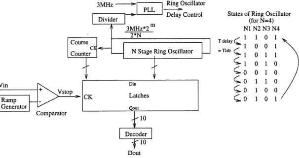
New Single Slope with Sub-nanosecond Time
Digitizer
The new single slope converter with a sub-nanosecond time digitizer is shown in Figure 4-2. The single slope part of the A/D is as described in Section 4.1 with a ramp generator and comparator. The time digitizer uses a gate delay to set the resolution of the converter (tlsb)[16]. This gate delay is controlled by phase locking the ring oscillator to a lower frequency system clock, often at the conversion rate of the A/D. If there are N stages in the ring oscillator, there are 2N possible states of the ring oscillator. Thus, the ring oscillator provides the least significant ln2 2N = 1+ In2 N
bits and the coarse counter provides the remaining bits. This architecture makes the speed and resolution performance of the A/D independent of the availability of a high frequency, low noise, on-chip clock. The maximum frequency on chip is now 2, where N is the number of stages in the ring oscillator, and m is the number of bits
of resolution. Additionally, using a gate delay as the time measurement unit allows the resolution of the time digitizer and thus the overall performance of the A/D to improve with technology scaling.
Another interesting feature of the single slope converter is the tradeoff between conversion rate and number of bits for a given tlsb. This tradeoff is depicted in Figure 4-3. 10b can be resolved at 3MHz using tlsb=325psec. Or, 9b can be resolved at
6MHz using the same tIsb. The Phase Locked Loop (PLL) and ring oscillator frequency stay the same. The A/D converter could potentially be programmable along this resolution/speed curve at minimal additional hardware cost. At high resolutions (low conversion frequencies), the accumulation of jitter will reduce the effective number of bits. However, there is still a linear tradeoff between dynamic range and speed.
At 12MHz, tlsb=81psec, which is too fast for 0.35um technology given variations in temperature, process and power supply. Sub-gate delay resolution has been obtained in [16] and [17]. These extensions will be elaborated on in Chapter 9.
States of Ring Oscillator (for N=4) N1 N2 N3 N4 =Tl delay 1 0 1 = 1 0 1 1 o 1 0 S0 1 0 O 1 1 o0 0 1 0 0 0 1 0 1 Vin V+n Vst< Ramp Generator Comparator Dout
Figure 4-2: New Single Slope Architecture with Subnanosecond Time Digitizer
S..
m m
1024 Tlsb's=10 bits in 1
3MHz
1
512 Tlsb's=9 bits inFigure 4-3: Linear Tradeoff Between Resolut6MHz
Figure 4-3: Linear Tradeoff Between Resolution and Speed
TlsbEFl_
4.3
Calibration
Calibration of the A/D can be performed at the end of each line of the image during the 35 pixel period blanking interval. The proposed calibration technique consists of measuring and storing the digital value of the comparator delay. This delay is subtracted from the digital output of the converter. Then, the full scale input voltage is applied. The slope of the ramp is adjusted to achieve Dmax when the input is full scale. The effect of this calibration is shown in Figure 4-4. This calibration scheme only aligns the endpoints of the A/D transfer curve. Since no calibration is performed in the middle of the curve, the A/D must be designed for good linearity. This translates to the need for a linear ramp generator.
Dmax 0
Dout
ramp slopeS
change 0 VfsChapter 5
Design of a 10b, 3 MS/s Single
Slope A/D
5.1
Introduction
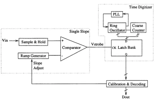
The new single slope architecture described in Chapter 4 is detailed in Figure 5-1. The single slope compares the input voltage to a ramp to generate Vstrobe. The time digitizer uses Vstrobe to latch the state of a ring oscillator and coarse counter. The final output is decoded from the latch bank. Endpoint calibration is performed during the blanking intervals at the end of each line and at the end of each frame by adjusting the slope of the ramp.
This chapter details the design of the analog blocks in Figure 5-1. Design choices are motivated by the minimization of power and area. The analog blocks include the time digitizer, track and hold, ramp generator, and comparator. Bias point generation and critical timing issues are also discussed.
Time Digitizer
-Vin
Dout
Figure 5-1: Single ended representation of Single Slope Architecture
5.2
Time Digitizer
5.2.1
Overall Architecture
A high resolution time digitizer is a critical part of increasing the conversion rate
of time based A/D converters. In the architecture shown in Figure 5-2, the state of a phase locked ring oscillator gives the least significant 1 + ln2 N bits (where N is the
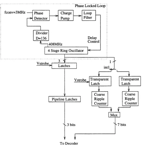
number of ring oscillator stages), while a coarse counter provides the most significant bits. The resolution of the time digitizer is given by tlab = where N is the number of stages in the ring oscillator, D is the divider ratio, and f, is the conversion rate of the A/D. t1ib is the delay of a single ring oscillator stage, and the minimum value of tl8b will scale with smaller feature sizes. Thus the achievable performance of this A/D architecture (in terms of resolution and conversion rate) follows technology scaling curves. The divider ratio, D, can be changed depending on the value of N and
f,. Given fe, N is chosen based on power, area, and noise considerations.
Area stays approximately fixed over a small range of increasing N. This is be-cause the small area of the ring oscillator increases, but the area of the coarse counter decreases. Power, however, increases with increasing N. This is because the ring
os-Phase Locked Loop :
fconv=3MHz Phase Charge Loop
Detector S e Pump O Filter
Divider
D=136 Delay
Control
408MHz
4 Stage Ring Oscillator
To Decoder
cillator is implemented using fully-differential current-steering circuits to minimize noise caused by and coupled into the ring oscillator. Each ring oscillator stage dis-sipates static power, as do the extra fully-differential buffers and fully-differential to single ended converters. The fewer the number of ring oscillator stages, the faster the frequency of the oscillator and the more dynamic power is dissipated in the ring oscillator and coarse counter. There is a tradeoff between static power dissipated in the ring oscillator and dynamic power in the single ended coarse counter. A four stage ring oscillator was chosen to make the static power dissipated in the ring oscillator approximately equal to the switching power dissipated in the coarse counter. The four stage ring oscillator was made by connecting three inverters and a buffer in a
chain, as shown in Figure 5-3.
The four stage ring oscillator has 8 possible states of nominally equal duration as shown in Figure 4-2. The least significant 3 bits are resolved. The divider value D for the phase locked loop is 136 given a system clock at the conversion rate of 3MHz.
The frequency of oscillation of the ring oscillator is 408 MHz. This gives a tlsb of
306psec and an overcount of 1 - 1024 * tlsb or 19.6nsec. The overcount allows for
the delay through the comparator and time needed to reset the ramp and track and hold.
Two ripple counters are interleaved to form the coarse counter as in Figure 5-2. This gives the transparent latch time to resolve the input from the ring oscillator and the coarse counter time to ripple that decision through. Since the two counters are interleaved, this resolution and ripple time does not deduct from the conversion time. The fine outputs are pipelined to match the latency in the coarse ripple counter and to increase the time for resolving the LSBs.
Section 5.2.2 describes the circuit design and issues involved in the ring oscillator and phase locked loop. Prominent issues include mismatches which cause DNL, jitter analysis and minimization, power reduction, and designing the loop to lock under all process, temperature and supply variations. Section 5.2.3 describes the fully-differential latches used to latch the state of the ring oscillator. Section 5.2.4 details the interleaved coarse counter implementation.
5.2.2
Ring Oscillator and Phase Locked Loop
The overall block diagram for the phase locked ring oscillator is shown in Figure 5-3. One output of the oscillator is buffered and converted from a fully-differential to a single ended signal. The divider was implemented in a single ended fashion. The output of the divider is fed to a phase detector with an off chip reference clock running at fe=3MHz. The phase detector then causes the charge pump to pump up or down, depending on the phase error between the output of the divider and the off chip reference clock. The charge pump circuit pumps current into a loop filter, which changes the control voltage that determines the ring oscillator frequency. A higher frequency clock could also be used as the reference clock, if available on chip.
fc=3M
z
Single Ended Fully Differential
Figure 5-3: Phase Locked Loop Block Diagram
Ring Oscillator
A schematic of one fully-differential ring oscillator stage for the time digitizer
is shown in Figure 5-4. The ring oscillator frequency is controlled by Vdelaycontrol changing the current through M20. M1 and M2 form a current-steering NMOS source-coupled pair with diode connected PMOS load devices. The output is shown such that this stage is an inverter. The output terminals are simply flipped for a non-inverting buffer connection, as in the last stage of the ring oscillator shown in Figure 5-3.
The output swing at the drains of M3 and M4 changes over temperature, process and supply by about 0.5Volts. This swing variation imposed some extra design chal-lenges to subsequent circuits. Another solution would have been to actively bias M3
Vin
Vdela
Tdelay = 306 psec
Fully Differential Swing = IV, nominal
Device W/L
M 1,M2 4/0.36
M3,M4 1.52/0.4
M20 2/0.88
when locked
Figure 5-4: Ring Oscillator Stage
and M4 in triode, using a replica bias circuit for the gate voltages of M3 and M4 to keep the output swing of the ring oscillator constant [18].
A potential problem in this design is mismatch between the input-referred offset voltage of different oscillator stages causing a fixed difference in delay. This mismatch translates directly into variations in time measurement units, and results in DNL. Since M1 and M2 are minimum size, it can be expected that they have a large threshold mismatch. Using a worst case estimate of a 10mV mismatch and multiplying by the inverse of the simulated output edge rate of the stage near switching gives a delay mismatch of 23psec. This translates to 0.08LSB DNL ( 23_ps). The channel lengths of M1 and M2 could be increased to minimize this mismatch induced DNL, but then more power (current through M20) would be needed to achieve the same delay. Since 0.08LSB DNL is sufficiently smaller than the 0.5LSB DNL specification, the channels of Ml and M2 were designed at minimum length to minimize power.
Mismatches in the M20 w's of different stages can cause different currents between stages. This current difference translates into a time delay difference, and also results in DNL. However, M20 was designed with twice minimum channel length and width to reduce mismatches. Careful, symmetric layout was also done on the ring oscillator stages to reduce mismatches.
Jitter is an uncertainty in the delay of the ring oscillator stage. This uncertainty is caused by supply noise and thermal noise in the MOSFETS. Jitter is a time varying error that contributes to the noise floor of the A/D and reduces the converters effective
number of bits (ENOB). Assuming that jitter should be less than quantization noise (0.3LSB RMS [7]) gave a jitter specification of less than 0.15LSB RMS. Multiplying this by TLSB = 306psec and dividing by 1024 gave a 1.5 P RMS jitter spec. The jitter was divided by i-024 because in the worst case, jitter is accumulated in quadrature over 1024 delays for a 10 bit measurement. This assumes that jitter in each stage is uncorrelated and that noise processes are rapidly varying.
Jitter due to thermal noise in the ring oscillator stage of Figure 5-4 was simulated. A small signal noise analysis was performed to obtain a value for the RMS output voltage noise at the buffer stage switching point. This voltage value was multiplied by the inverse of the edge rate of the oscillator to approximate a delay uncertainty. This simulated uncertainty was 0.7 psec per stage, a factor of two lower than the specification.
As the resolution of the converter is increased, jitter will start to degrade the effective number of bits. At a resolution of 14 bits, noise caused by jitter becomes on the order of quantization noise. Although this diminishes the advantages of the linear tradeoff between conversion rate and resolution (ENOB) as described in Chapter 4, there is still a linear tradeoff between conversion rate and dynamic range.
Buffer
The fully-differential circuit shown in Figure 5-5 buffers the output of each ring oscillator stage. The buffers provide the ring oscillator with protection from kickback due to the operation of subsequent circuits, such as the latches or fully-differential to single ended converters.
Transistors M3 and M4 are biased in the triode region by grounding their gates. Again, the output swing of the buffers varies over process, temperature and supply. The buffers were designed to have slightly larger swing than the ring oscillator to ensure that there is enough signal to trigger the differential to single ended converters over these variations. Matching between buffer stages is important so that delays are the same and DNL is minimized. Assuming, as above, a worst case 10mV mismatch in threshold voltages, the DNL error due to buffer mismatch should be less than
Fully Differential Swing = 1.2V, nominal Device W/L M1,M2 10/0.36 M3,M4 2/0.6 M20 10/1.6 Vi from Ring Figure 5-5: Buffer
O.1LSB. To minimize bias current mismatch, the current source transistor, M20, was designed to have a long channel length. Additionally, layout of the buffers was as symmetric as possible.
Differential to Single Ended Converter
The differential to single ended converter in Figure 5-6 converts the output of the ring oscillator buffer to a single ended signal for the phase locked loop (PLL) divider.
Vdd Vout single ended Vin from Buf: Device M1,M2 M3,M4 M20 Device M5 M6 W/L 10/0.36 2/0.72 W/L 1/0.36 2/0.4 4/0.7 Device M7,9,11 M8,10,12 W/L 1/0.36 2/0.4
Figure 5-6: fully-differential to single ended converter
In the circuit of Figure 5-6, the input source-coupled pair with active load (Ml-M4) acts as an open loop op amp that converts the fully-differential signal to a
higher swing single-ended signal at node ol. Source follower M5-M6 level shifts ol to be symmetric around the switching voltage of inverter M7-M8. Since the swing of the fully-differential input changes over temperature, process and supply variations, the swing of the single ended outputs ol and o2 varies too. Care was taken to ensure that the swing of o2 included the switching point of the subsequent inverter chain over process, temperature, and supply variations.
Divider
The divide-by-136 in Figure 5-3 divides the ring oscillator 408MHz oscillation down to 3MHz for comparison to the system clock. The divide by 136 was imple-mented as shown in Figure 5-3 with three divide by twos and a divide by 17. There was a tradeoff between dynamic power in a single ended, full swing CMOS divider given by
PSingle-Ended r C * Vd2d
f
(5.1)
and power in a fully-differential, low swing divider given by
PFully-Differential ^ StaticPower(constant) + C * Vdd * V,, * f (5.2)
Where V,, is the fully-differential output swing. At low frequencies, a full-swing, single ended divider will consume less power than a low-swing, fully-differential di-vider. At higher frequencies, the dynamic power of a single-ended implementation may approach the static power of a low swing, fully-differential divider. Thus, op-erating frequency determines if a fully-differential or single ended implementation saves power. A design tradeoff can be made where the high frequency stages are differential and the low frequency stages are single ended. A low-swing, fully-differential implementation also has the advantage of minimizing the effect of switch-ing noise coupled into the divider. In this design, the divider frequencies were low enough so that a full-swing single ended divider saves power over a low-swing, fully-differential divider. If the resolution of the converter were increased, or the number
of ring oscillator stages decreased, the frequency may become high enough that a low-swing, fully-differential divider makes sense.
Vout fout= fi n
Figure 5-7: Single ended divide by 2
The single ended divide by two is shown in Figure 5-7. A standard cell T flip flop is used. On every period of Vin, Vout transitions from high to low or vice versa. This gives a division of two between the frequency of the input and the frequency of the output.
Vin
Tin
Vin
iUUuil
uuIJUli
J
Vout
I
F
<
9*Tin <_ 8*Tin Figure 5-8: Divide by 17
The single ended divide by 17 of Figure 5-8 is based on [19]. Four divide by 2 circuits, implemented as shown in Figure 5-7, divide the input by 16 when Q is high
(M1 is on, M3 is off, and M2 and MO function as an inverter). However, on every cycle, when the "count" of the divider gets to a certain value, Q goes low for one cycle, causing M1 to turn off and M3 to turn on. This keeps the input to the divide by 2 chain high until the flip flop is clocked again. Thus, one period of the input
pulse is skipped. The duty cycle (d = -) of the output shown in Figure 5-8 does not affect PLL operation since the subsequent phase detector is only sensitive to the falling edges of its input.
Phase Detector
VCO too slow
I I VCo -LJ
L
Reference _] L-Up
•
-
-L
U-p Down P Loop Locked VCO Reference Down Up L Down J L from dividerFigure 5-9: Phase Detector
The phase detector shown in Figure 5-9 compares the negative edges of V,,f and VCO. Up and Down output signals are activated for a duration proportional to the phase error between Vref and VCO. These Up and Down pulses indicate if the charge pump should pump the control voltage up or down.
Two examples are shown in Figure 5-9. In the top example, the VCO frequency is lower than the reference frequency and the phase detector indicates that the charge pump should pump up. In the bottom example, the VCO and reference frequency are locked and the phase detector outputs short up and down pulses.
The phase detector must output these short up and down pulses when locked to avoid a "dead zone" in the phase detector transfer characteristic, as shown in the solid line of Figure 5-10. The phase detector transfer curve plots the phase error, Oe