broadband photoresponse in graphene-2D
semiconductor lateral heterojunctions
The MIT Faculty has made this article openly available.
Please share
how this access benefits you. Your story matters.
Citation
Yuxuan Lin et al. "Asymmetric hot-carrier thermalization and
broadband photoresponse in graphene-2D semiconductor lateral
heterojunctions." Science Advances 5, 6 (June 2019): eaav1493 ©
2019 The Authors
As Published
http://dx.doi.org/10.1126/sciadv.aav1493
Publisher
American Association for the Advancement of Science (AAAS)
Version
Final published version
Citable link
https://hdl.handle.net/1721.1/121449
Terms of Use
Creative Commons Attribution NonCommercial License 4.0
A P P L I E D P H Y S I C S
Asymmetric hot-carrier thermalization and broadband
photoresponse in graphene-2D semiconductor
lateral heterojunctions
Yuxuan Lin1*, Qiong Ma2*, Pin-Chun Shen1*, Batyr Ilyas2, Yaqing Bie2, Albert Liao1,
Emre Ergeçen2, Bingnan Han1,3, Nannan Mao1, Xu Zhang1, Xiang Ji1, Yuhao Zhang1, Jihao Yin3,
Shengxi Huang4, Mildred Dresselhaus1,2†, Nuh Gedik2, Pablo Jarillo-Herrero2, Xi Ling5‡,
Jing Kong1‡, Tomás Palacios1‡
The massless Dirac electron transport in graphene has led to a variety of unique light-matter interaction phenomena, which promise many novel optoelectronic applications. Most of the effects are only accessible by breaking the spatial symmetry, through introducing edges, p-n junctions, or heterogeneous interfaces. The recent develop-ment of direct synthesis of lateral heterostructures offers new opportunities to achieve the desired asymmetry. As a proof of concept, we study the photothermoelectric effect in an asymmetric lateral heterojunction between the
Dirac semimetallic monolayer graphene and the parabolic semiconducting monolayer MoS2. Very different hot-
carrier cooling mechanisms on the graphene and the MoS2 sides allow us to resolve the asymmetric
thermaliza-tion pathways of photoinduced hot carriers spatially with electrostatic gate tunability. We also demonstrate the potential of graphene-2D semiconductor lateral heterojunctions as broadband infrared photodetectors. The pro-posed structure shows an extreme in-plane asymmetry and provides a new platform to study light-matter inter-actions in low-dimensional systems.
INTRODUCTION
Breaking spatial symmetry in materials like graphene is a powerful tool to enhance or even induce new forms of light-matter interactions (1). For instance, edges and grain boundaries in graphene samples have been used to control surface plasmons (2–4). At the same time, electrostatic-gated homojunctions enable the hot carrier–mediated photothermoelectric (PTE) effect in graphene (5–8). An additional degree of freedom is given by vertical heterostructure assembly (9) of two-dimensional (2D) materials through aligned layer-by-layer stacking. This has made it possible not only to leverage the asymmetry in the out-of-plane direction but also to design artificial lattices with engineered symmetry through twisted angles between the layers (10–12). All of these have allowed the recent discovery of many pre-viously unidentified light-matter interaction phenomena on 2D ver-tical heterostructures, including interlayer excitonics/valleytronics (13, 14), photoexcited thermionic emission/tunneling (15, 16), fluores-cence intermittency (17), and tunable twisted-angle circular dichroism (18). In parallel, several groups have developed synthetic methods for lateral heterostructures with precise spatial confinement through either selective seeding or epitaxy, which further extended the de-sign space for multifunctional and high-performance electronic and optoelectronic devices and systems based on 2D heterostructures (19–29). One good example is the tunable photoluminescence (PL)
emissions induced by the epitaxial strain in WS2-WSe2 coherent
super-lattices (29). In spite of all this remarkable progress, the light-matter interactions of highly asymmetric lateral heterojunctions such as those between graphene and 2D semiconductors have not been explored.
Here, we aim to study the photoelectric response at graphene-2D semiconductor lateral heterojunctions. The massless Dirac transport in graphene leads to a unique hot-electron PTE effect (5–8, 30). Be-cause of the ultrafast electron-electron scatterings (on the order of 10 fs) (31, 32) and relatively slow electron-phonon scatterings (on the order of picoseconds) (33–37), the photoinduced carriers are thermalized by the electronic system and dissipate the heat very slowly to the lattice. In a conventional semiconductor with parabolic elec-tronic dispersion, on the other hand, the photoinduced electrons and holes either are separated and collected directly by a built-in electric field [the photovoltaic (PV) effect] or scatter strongly with phonons and impurities and transfer their kinetic energy to heat or lattice vibrations. If the Dirac semimetallic graphene and the parabolic 2D semiconductor are put in close proximity with each other within the 2D plane, then the vast asymmetry of the energy transfer path-ways on the two sides gives rise to very interesting features that can be addressed spatially through localized light excitation. In this work, we demonstrate such asymmetric hot-electron thermalization on a synthetic graphene-MoS2 lateral heterojunction. From gate-dependent
scanning photocurrent measurement, we were able to confirm that the PTE effect dominates the photoresponse at the lateral junction when the excitation photon energy is below the MoS2 bandgap. A
theoretical model was built to understand the asymmetric thermal-ization pathways of the photoinduced hot carriers at the junction, which matched our experimental observations very well. Spectral photoresponse measurements also suggested that the graphene-MoS2
lateral heterojunction could potentially be used as a broadband in-frared detector. Our proposed asymmetric lateral heterostructure provides a new platform to study novel light-matter interactions in 1Department of Electrical Engineering and Computer Science, Massachusetts
Insti-tute of Technology, Cambridge, MA 02139, USA. 2Department of Physics, Massachusetts
Institute of Technology, Cambridge, MA 02139, USA. 3School of Astronautics, Beihang
University, Beijing 100191, China. 4Department of Electrical Engineering, The
Pennsylvania State University, University Park, PA 16802, USA. 5Department of
Chemistry and Division of Materials Science and Engineering, Boston University, Boston, MA 02215, USA.
*These authors contributed equally to this work. †Deceased.
‡Corresponding author. Email: xiling@bu.edu (X.L.); jingkong@mit.edu (J.K.); tpalacios@ mit.edu (T.P.)
Copyright © 2019 The Authors, some rights reserved; exclusive licensee American Association for the Advancement of Science. No claim to original U.S. Government Works. Distributed under a Creative Commons Attribution NonCommercial License 4.0 (CC BY-NC). on June 27, 2019 http://advances.sciencemag.org/ Downloaded from
2D materials, especially for those that can be enhanced by spatial symmetry breaking, such as photoelectric and plasmonic effects in graphene and exciton transports in 2D semiconductors.
RESULTS AND DISCUSSION
Figure 1A shows a schematic of the lateral graphene-MoS2
hetero-junction device. The graphene-MoS2 lateral heterostructures were
obtained through the seeding promoter–assisted chemical vapor deposition (CVD) that we developed previously (see Materials and Methods for details) (25, 38). Atomic force microscopic (AFM) images, high-resolution transmission electron microscopic (HRTEM) images, and Raman and PL mappings (figs. S1 to S3) at the graphene- MoS2 interfaces confirm that the two materials overlap only a few
tens of nanometers at the interface (25). Note that such a nanometer- scale overlap does not substantially affect the photoresponse at the interfaces because the optical excitations cannot resolve any struc-tural features that are below the wavelengths, and both the depletion width (on the order of 100 nm) (39) in a PV effect and the cooling length (on the order of 100 nm to 1 m) (5, 7, 36) in a PTE effect are sufficiently larger than the size of the overlaps. Figure 1B shows the optical microscopic image of the graphene-MoS2 lateral
hetero-junction device. We fabricated multiple long and short electrodes near the graphene-MoS2 interface to perform transport and
photo-current measurement on both the lateral junction and each homo-geneous material. All the devices were fabricated on top of a 285-nm
SiO2/Si wafer, and the Si substrate served as a back gate. Figure 1C
plots the transfer characteristics for devices fabricated on the graphene layer, on the MoS2 layer, and across the interface (channel current, Ich,
versus back-gate voltage, Vg). The charge neutrality point of graphene
is around 3 V, whereas the threshold voltage of MoS2 is very
nega-tive (around −17 V). The weak nonlinearity of the output character-istics (channel current, Ich, versus channel voltage, Vch, with various
Vg), as shown in fig. S4, indicates that the Schottky barrier height at
the graphene-MoS2 interface is relatively low (on the order of 10 meV;
see fig. S10), which has also been confirmed by our previous work (25) and others (26, 27). Such a weak Schottky junction suggests that the PV effect, if any, would be very weak at the graphene-MoS2
inter-face. Figure 1D shows a scanning photocurrent microscopic (SPCM) image of the device with a 633-nm laser excitation (see Materials and Methods for experimental setups), from which it is observed that the strongest photocurrent response is localized at the graphene- MoS2 junction. The I-V curves with the 633-nm light shined on the
junction, as shown in fig. S5, indicate that there is an electromotive force generated, which rules out any photoconductive or bolometric effect.
Now, let us consider the PTE effect. The photoexcited carriers are first thermalized through either electron-electron scattering or electron-phonon scattering, leading to broader energy distributions of electrons. On the graphene side, because of the linear electronic dispersion and its low dimensionality, the electron-electron scatter-ings are substantially stronger than the electron-phonon scatterscatter-ings
Graphene MoS2 Junction T = 100 K –40 –20 0 20 Vg(V) Ich () m µ/ A µ 0 0.5 1 1.5 A B C D 633 nm Ri 20 0 –20 G M 5 µm MoS2 Graphene MoS2 Graphene ×0.1 A B C D B C G – + M X Dirac semimetal (graphene) Parabolic semiconductor (MoS2) EF Photon Electron Phonon EF E (µA/W)
Fig. 1. Graphene-MoS2 lateral heterojunction photodetector. (A) Schematic of the device. (B) Microscopic image of the as-fabricated device on a 285-nm SiO2/Si
sub-strate. Multiple long and short electrodes (Ni/Au) were placed around the lateral junction to probe different regions of the device electrically. The inset diagram indicates the cathode and the anode of the device for the electrical and photocurrent measurements; the axis indicates the direction of the x axis for the X-Vg mappings and the
simulation results. (C) Transfer characteristics of the graphene-MoS2 junction (orange, current applied across electrodes B and C and voltage probed across the short
electrodes), MoS2 (green, across electrodes C and D), and graphene (red, across electrodes A and B), respectively. The channel voltage Vch = 0.1 V. (D) Spatial
photorespon-sivity (Ri = Iph/Pin, with Iph and Pin denoting the photocurrent and the incident light power, respectively) of the device under a 633-nm laser excitation with Vch = 0 V and
Vg = 0 V. The dotted lines indicate the channel (in white) and electrodes (in orange) of the device. “G” and “M” are short for graphene and MoS2, respectively. (E) Schematics of
the dominating hot-electron cooling processes (top) and the spatial hot-electron thermalization pathways (bottom) of the Dirac semimetallic graphene (left) and the parabolic semiconducting MoS2 (right). In the bottom panels, the arrows indicate possible heat transfer paths, and the diameters of the purple cylinders connecting the
electron, the lattice, and the substrates indicate the strength of thermal couplings.
on June 27, 2019
http://advances.sciencemag.org/
(including scattering with optical phonons, acoustic phonons, and disorder-assisted supercollisions; see the Supplementary Materials for a detailed discussion) (33–37). Consequently, electrons in graphene would not reach thermal equilibrium with the lattice before being collected (Fig. 1E, left), given that the cooling length of hot electrons in graphene is typically hundreds of nanometers to micrometers (5, 7, 36). On the MoS2 side, however, the electronic dispersion at
the band edge is parabolic, in which the electrons and lattices are always in thermal equilibrium because of the much stronger electron- phonon scatterings (Fig. 1E, right, and the Supplementary Materials). Such an asymmetric behavior of heat dissipations on the two sides of the graphene-MoS2 junction could lead to very asymmetric
tem-perature distributions and unusual photocurrent profiles, which will be discussed later. The increased electron temperature at the graphene-MoS2 junction (hot side) with respect to the electrodes
(cold side) could then be transduced into an electric signal through the Seebeck effect, and the photovoltage is given by Vph = −(Sgr − SMoS2)·Tjel,
with Sgr and SMoS2 representing the Seebeck coefficients of graphene
and MoS2, respectively, and Tjel denoting the increase of electron
temperature at the graphene-MoS2 junction with respect to the
temperature of the unheated substrate. The Seebeck coefficient of graphene follows a nonmonotonic relation with respect to the Fermi level or gate voltage (5, 7, 36). Given that SMoS2 changes very slowly
and monotonically with the gate voltage when MoS2 is heavily doped,
the photovoltage induced by the PTE effect should approximately
follow the nonmonotonic trend of Sgr with gate voltage. Meanwhile,
the photovoltage induced by the PV effect should change mono-tonically with the gate voltage simply because the change of the bar-rier height at the junction is positively correlated to the difference between the Fermi level shifts of graphene and MoS2, which could
only change monotonically with a global gate voltage.
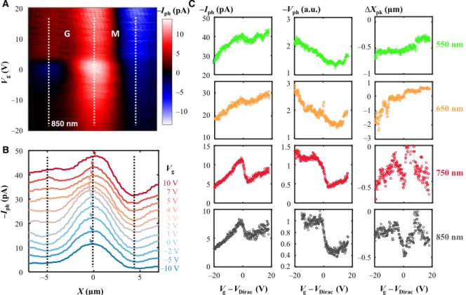
Gate-dependent SPCM measurements were carried out to con-firm that the PTE effect is dominant in the graphene-MoS2 lateral
heterojunction. Figure 2A shows the photocurrent mapping for an 850-nm laser beam sweeping along the linecut across the junction shown in Fig. 1D as the x axis while the gate voltage varying for each laser position sweep as the y axis. In addition to the main photocur-rent peak at the graphene/MoS2 interface, we also observed two extra
peaks at the graphene-metal and the MoS2-metal junctions. While
the photocurrent at the MoS2-metal junction increases
monotoni-cally with the gate voltage, the photocurrent at the graphene-metal junction follows an S-shape curve with the gate voltage (fig. S6). We also observed that the photocurrent at the graphene-MoS2
junc-tion undergoes a very nonmonotonic change with respect to the gate voltage around the charge neutrality point of graphene. This can be seen more clearly in Fig. 2B, as we stack the gate-dependent photocurrent line profiles on top of each other. The peak photocur-rent and the corresponding photovoltage as a function of the gate voltage for four different excitation wavelengths are plotted in the first and second columns of Fig. 2C, where the photovoltages are
A B C –Iph(pA) G M 850 nm Vg (V) –10 –5 0 5 10 –20 0 10 20 –10 –10 V –5 V –2 V 0 V 1 V 2 V 3 V 4 V 5 V 7 V 10 V Vg X (µm) –Iph (pA) –5 0 5 0 10 20 30 40 50
Vg–VDirac(V) Vg–VDirac(V) Vg–VDirac(V)
–20 0 20 –20 0 20 –20 0 20 0 5 10 0 5 10 15 10 20 30 20 30 40 50
–Iph(pA) –Vph(a.u.) ∆Xpk(µm)
1 2 3 1 2 3 0 0.5 1 1.5 0.4 0.6 0.8 1 0.2 –1 –0.5 0 –2 –1 0 1 –3 –0.5 0 –0.5 0 550 nm 650 nm 750 nm 850 nm
Fig. 2. Gate-dependent SPCM measurements of the device. (A) Gate voltage (Vg)–linecut (X) mapping of the photocurrent (Iph) under an 850-nm laser excitation. The
three dotted lines indicate (from left to right) the junctions of metal-graphene, graphene-MoS2, and MoS2-metal. The magnitude of Iph was flipped to make the
photore-sponse at the graphene-MoS2 junction positive. (B) Stacked linecuts along the x axis of Iph with different Vg. The arrows indicate the peak positions. (C) Peak photocurrent
Iph (left column), peak photovoltage Vph (middle column), and peak offsets Xpk (right column) as a function of the gate voltage with respect to the charge neutrality point
of graphene (VDirac), extracted from the Vg-X mappings with laser excitations of 550 nm (first row), 650 nm (second row), 750 nm (third row), and 850-nm (fourth row). Vph
is estimated by Iph·Rdark = Iph·Voffset/Idark, in which the dark resistance Rdark is inversely proportional to the dark current Idark averaged throughout the points whenever the
laser spot is off the device in the Vg-X mappings, assuming that a constant voltage offset Voffset is supplied by the measurement setup. a.u., arbitrary units.
on June 27, 2019
http://advances.sciencemag.org/
obtained by multiplying the photocurrent value by the resistance of the junction. With shorter excitation wavelengths (550 and 650 nm) or photon energies above the bandgap of MoS2, both the
photocur-rent and the photovoltage change monotonically with the gate voltage, whereas an S-shaped relation was observed with longer excitation wavelengths (750 and 850 nm) or photon energies below the bandgap of MoS2. Given that such an S-shaped photovoltage trend matches
well with the trend of the Seebeck coefficient change of graphene as a function of the gate voltage (5, 7), we concluded that the photore-sponse mainly originates from the PTE effect, especially at longer wavelengths.
The lateral geometry and the asymmetry of the graphene-MoS2
junction also make it possible to access different positions around the junction with light excitation. As a result, the spatial patterns due to the vast discrepancy of the thermalization pathways toward the two sides can be revealed. As shown in Fig. 2B and the third column of Fig. 2C, the photocurrent peak position was observed to undergo an unusual shift toward the graphene side by up to 500 nm as the graphene reaches its charge neutrality. This effect could be observed clearly at longer excitation wavelengths (750 and 850 nm). Note that no obvious shifts around graphene’s charge neutrality volt-age were observed on the graphene-metal or the MoS2-metal
junc-tion (fig. S6). Given that the incident light power is relatively low, the Seebeck coefficients would not be affected by the laser position to the first-order approximation. As a result, the photocurrent profile should follow the profile of the electron temperature change at the lateral junction as we move the laser beam position across the junction.
The photoinduced distribution of electron temperature is gov-erned by the heat transfer equation (5, 7, 40): ∇2Tel − g(Tel − T0) +
pin = 0, in which and g represent the lateral 2D thermal
conductiv-ity and the vertical heat loss, respectively; Tel is the electron tem-perature at a given position; T0 is the temperature of the substrate;
and pin is the input power density, which is provided, in our case, by
the incident laser beam. On the MoS2 side, the total thermal
con-ductivity tot and the heat loss into the substrate gsub should be con-sidered as the dominant terms, given that electrons and lattices are considered as a whole, as they are always in thermal equilibrium (Fig. 1E, right). On the graphene side, in contrast, electrons are thermally insulated from the lattice very well, so electron thermal conductivity el and the thermal coupling between electrons and
lattices gel-L = Cel with and Cel representing the electron-lattice cooling rate and electron heat capacity, respectively, govern the heat dissipation and hence determine the electron temperature distribu-tion (Fig. 1E, left). As given in more details in the Supplementary Materials, the typical values of the g and ratios are gel-L/gsub = 10−5 to 10−1 and
grel/MoS2tot = 0.01 to 1.5, which gives rise to much stronger
heat dissipations toward the MoS2 side than toward the graphene
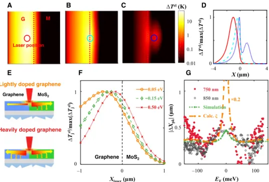
side. Figure 3 (A to D) and fig. S14 show the simulated 2D tempera-ture distributions and 1D linecuts across the junction of the device as the laser shines at the graphene, the graphene-MoS2 junction,
and MoS2 (see the Supplementary Materials for more details about
the simulation). It is clearly observed that the peak electron tem-perature becomes much higher when the laser shines on the graphene side, which matches the aforementioned discussion about the asymmetric heat dissipation pathways. This also explains why the junction temperature Tjel may reach its maximum when the center
of the laser spot is away from the geometric junction, toward the graphene direction (Fig. 3F). The distance between the peak position of Tjel and the geometrical junction can be characterized by the
cooling length of hot electrons, given by = (el/ Cel)1/2. becomes
Lightly doped graphene
Heavily doped graphene
0.01 0.1 1 10 ∆Tel(K) Laser position G M X (µm) –4 0 4 ∆ T el/max(∆ T el) 0 1 Graphene MoS2 0.05 eV 0.50 eV 0.15 eV Xlaser(µm) –1 0 1 ∆ Tj el/m ax(∆ Tj el) 0 1 Simulation 850 nm 750 nm Calc. ξ ×0.2 EF(meV) –100 0 100 |∆ Xpk | (µm) 0 1 0.5 A B C D E F G Graphene MoS2
Fig. 3. Theoretical analysis of the thermalization pathways. (A to C) Simulated distributions of electron temperature increase (Tel) as the laser spot is on the graphene
side (A), the junction (B), and the MoS2 side (C). The circles indicate the center positions of the incident laser. (D) Linecuts of Tel along the x axis normalized to the
maxi-mum Tel as in (A) to (C). (E) Schematics of the heat dissipations of photoinduced hot electrons when graphene is lightly doped (with the graphene Fermi level E
F = 0.05 eV;
top) and heavily doped (EF = 0.5 eV; bottom). (F) Normalized electron temperature at the graphene-MoS2 junction with different EF. The dashed line indicates the geometric
junction. (G) Measured magnitudes of peak position offsets (|Xpk|) with 750-nm (filled circles) and 850-nm (open circles) laser excitations, as well as the simulated |Xpk|
and calculated electron-lattice cooling length on the graphene side (), as a function of EF.
on June 27, 2019
http://advances.sciencemag.org/
much bigger as the Fermi level (EF) of graphene moves toward the
charge neutrality point, as shown in figs. S13 and S14. The simulated electron temperature profiles at the junction as the laser spot moves across the junction when graphene is at (lightly doped case; see Fig. 3E, top) and away from (heavily doped case; see Fig. 3E, bottom) the charge neutrality are plotted in Fig. 3F, from which it is observed that the peak of the Tjel profile shifts ~400 nm farther away from
the geometrical junction in the lightly doped graphene case than that in the heavily doped graphene case. The trends of the cooling length, the simulated Tjel peak offset with various EF of graphene, and the
peak photocurrent offsets with 750- and 850-nm light excitations are plotted in Fig. 3G, which are in accordance with one another.
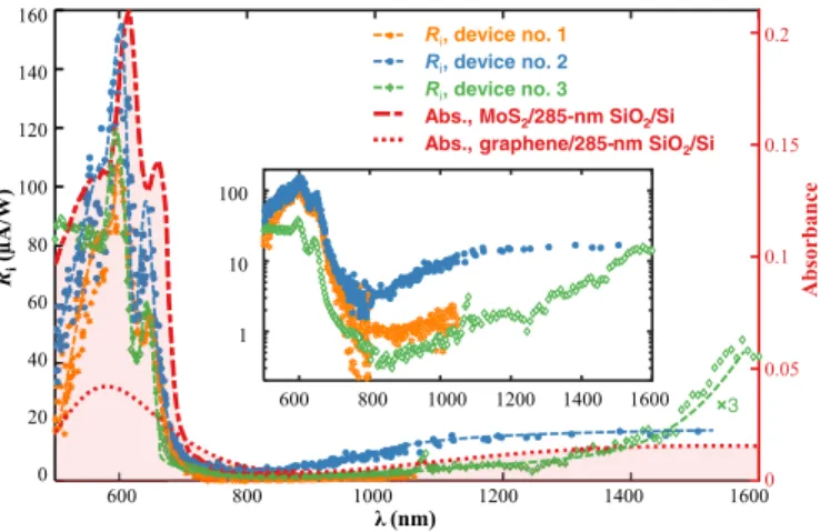
Last, we demonstrate the broad spectral range of photoresponses of such a graphene-semiconductor lateral heterojunction promised by the PTE effect. We observed strong photoresponse localized at the graphene-MoS2 lateral junction from SPCM mappings with a
variety of wavelengths ranging from visible to short-wave infrared range (Fig. 1D and fig. S9). In Fig. 4, the spectral photoresponsivity of three different devices is also exhibited. The response at shorter wavelengths (below 700 nm) follows the absorbance of MoS2, whereas
the response at longer wavelengths (above 700 nm) matches better with the absorbance of graphene on a 285-nm SiO2/Si substrate.
This—combined with the different gate-dependent photocurrents, photovoltages, and photocurrent peak positions at shorter wave-lengths (550 and 650 nm) and longer wavewave-lengths (750 and 850 nm)— clearly indicates that the photoresponse with the excitation photon energies above and below the MoS2 bandgap is dominated by the PV
or photoconductive effect in MoS2 and the PTE effect in graphene,
respectively. Note that the photoresponsivity reaches its minimum at around 900 nm, which corresponds to the valley of the interfer-ence fringes of the substrate. No sign of cutoff was observed in the spectral range (from 500 to 1600 nm) of our measurements. Theo-retically, the spectral response of such a structure should be extended to at least 5 m, limited by the Pauli blocking of graphene (41). In addition, the photocurrent scaled linearly with the incident power among all the wavelengths, as shown in fig. S7A. Temperature- dependent measurements reveal a relatively weak nonmonotonic relationship between the photoresponsivity and the temperature
(fig. S7B), which can be explained by the competition between two hot-carrier cooling mechanisms, that is, acoustic-phonon cooling (dominant at low temperature) and disorder-assisted supercollision cooling (dominant at high temperature) (36). Gate-dependent SPCM measurements at different temperatures (fig. S8) reveal that the photocurrent peak position shifts reach maximum at intermediate temperature (50 to 100 K), in accordance with these competing hot- carrier cooling mechanisms as well. According to the ultrafast photo-current autocorrelation measurement, the intrinsic time constant of the photogeneration process was extracted to be ~14 ps. These ob-servations suggest that the graphene-2D semiconductor lateral hetero-junction can be potentially used as a broadband (visible to mid-infrared), ultrafast (~10 ps), and room temperature photodetector.
In summary, we have studied the photoresponse on an asym-metric lateral heterojunction between Dirac semimetal graphene and parabolic semiconductor MoS2 and have attributed the
broad-band photoresponse to the PTE effect. A theoretical model was built to describe the asymmetric thermalization pathways of the photo-generated hot carriers, which has successfully explained the spatial feature from experiments. Our study provides a new perspective to study light-matter interactions in low-dimensional systems and paves the way for novel optoelectronic applications with 2D hetero-structures. With a rational design of such an in-plane asymmetry, one could possibly study many new phenomena that were either forbidden or requiring more advanced instrumentation in a homo-geneous film, including exciton diffusion, dichroic spin-valley photo-current in 2D semiconductors, electron-electron scattering, and surface plasmon polaritons in graphene.
MATERIALS AND METHODS
Synthesis of graphene/MoS2 lateral heterojunctions
Graphene flakes were first mechanically exfoliated onto a piranha- cleaned SiO2/Si substrate by the Scotch tape technique. Before the
growth of MoS2, the exfoliated graphene was annealed at 350°C in Ar
[300 sccm (standard cubic centimeters per minute)]/H2 (100 sccm)
for 3 hours to remove the tape residues. The parallel stitching growth of monolayer MoS2 was enabled by a seeding promoter–diffusion–
mediated CVD method (25). Perylene-3,4,9,10-tetracarboxylic acid tetrapotassium (PTAS) molecules were used as the seeding promoter. The PTAS was coated onto two additional clean SiO2/Si pieces,
which served as seed reservoirs, from which seeding molecules could selectively diffuse onto the hydrophilic surface of the target substrate for the MoS2 lateral synthesis. The target substrate (SiO2/Si
wafer with the graphene flakes) was then suspended between those two PTAS-coated SiO2/Si seed reservoirs. All of these three
sub-strates were faced down and placed on a crucible containing molyb-denum oxide (MoO3; 99.98%) powder precursor. This MoO3
precursor was put in the middle of a 25.4 millimeter quartz tube as the reaction chamber, and another sulfur powder (99.98%) precursor was placed upstream, 14 cm away from the MoO3 crucible, in the quartz
tube. Before heating, the CVD system was purged using 1000 sccm of Ar (99.999% purity) for 5 min; then, 20 sccm of Ar was intro-duced into the system as a carrier gas. Next, the temperature of the reaction chamber was increased to 350°C with a rate of 30°C min−1 and held at that temperature for 10 min. The temperature was then increased to 610°C with a rate of 30°C min−1. The monolayer MoS2
parallel stitched on graphene was synthesized at 610°C for 3 min under atmospheric pressure. The temperature of the sulfur source
600 800 1000 1200 1400 1600 λ (nm) 0 20 40 60 80 100 120 140 160 Ri (µA/W ) 0 0.05 0.1 0.15 0.2 Absorbance ×3 Ri, device no. 1 Ri, device no. 2 Ri, device no. 3
Abs., MoS2/285-nm SiO2/Si
Abs., graphene/285-nm SiO2/Si
1 10 100
600 800 1000 1200 1400 1600
Fig. 4. Spectral photocurrent response of the devices. Left axis: Photocurrent responsivity (Ri) as a function of the wavelength of incident light () of three different
devices. Right axis: Calculated absorbance (Abs.) of MoS2 (red dashed line) and
graphene (red dotted line) on a 285-nm SiO2/Si substrate based on the complex
refractive indices from (42, 43). The inset plots the spectral responsivity in log scale.
on June 27, 2019
http://advances.sciencemag.org/
was kept at ~170°C during growth. Last, the system was cooled down to room temperature quickly using an electric fan. During the cool-ing process, 1000-sccm Ar flow was maintained in the chamber to re-move the reactants, preventing further unintentional reactions.
TEM characterization
The as-grown graphene-MoS2 heterostructure was transferred onto
a TEM grid (Quantifoil, no. 656-200-CU; Ted Pella Inc.) by the poly(methyl methacrylate) (PMMA) method. After transfer onto a TEM grid, the PMMA layer was removed under vacuum annealing at 350°C for half an hour. HRTEM characterization of the hetero-structure at the atomic scale was carried out on a JEOL ARM 200CF transmission electron microscope equipped with a cold field-emission electron source and two spherical-aberration correctors operated under an accelerating voltage of 80 kV to reduce radiation damage.
AFM and spectroscopy characterization
The AFM characterization was carried out on a Dimension 3100 instrument, commercially available from Veeco Instruments Inc. PL and Raman spectra were carried out on a HORIBA Jobin-Yvon HR800 system and a WITec alpha 300 confocal Raman microscope. The laser excitation wavelength for the PL and Raman measurements was typically 532.5 nm. The laser power on the sample was about 0.1 mW. A 100× objective was used to focus the laser beam. The spectral parameters were obtained by fitting the peaks using Lorentzian/ Gaussian mixed functions as appropriate.
Device fabrication
The graphene-MoS2 heterostructures were first transferred onto the
285-nm SiO2/Si substrates with PMMA as the handling supporting
layer and diluted hydrofluoric acid (HF) as the oxide etchant to separate the material from the growth substrate. Electron-beam lithography (EBL) and e-beam evaporation followed by a liftoff process were used to deposit 30-nm Ni/20-nm Au stacks as the ohmic contacts to both the graphene and the MoS2 sides. Another EBL and reactive ion
etching with oxygen plasma were used to define the channel area.
Electrical and photocurrent measurements
The transport measurements and spatial photocurrent mappings were carried out with a confocal laser scanning microscopy setup. The chips were wire-bonded onto a chip carrier and mounted in a Janis ST-500 helium optical cryostat equipped with electrical con-nections, a well-defined microscopic optical path, and a tempera-ture controlling system. The device was kept under high vacuum (<10−5 torr) throughout the measurements. Sourcemeters (Agilent B2902a), current preamplifiers (Ithaco DL1211), and data acquisi-tion cards (Naacquisi-tional Instruments PXI module) were used for the electrical sourcing and probing. Both the transport and the photo-current measurements were performed at 100 K if not mentioned explicitly in the text. For the scanning photocurrent measurements, a broadband supercontinuum fiber laser (Fianium) was combined with a monochromator to generate the monochromic laser beam with the desired wavelength (tunable from 400 to 1600 nm). A two- axis piezo-controlled scanning mirror was coupled to a microscope objective through two confocal lenses to perform the spatial scan-ning with the laser beam spot of around 1 m on the device. The photocurrent and the reflected light intensity were recorded simul-taneously to form the scanning photocurrent images and the reflec-tance images. All the photocurrent results were measured under the
short-circuit condition, in which zero voltage bias was applied across the device. The photovoltage corresponds to the open-circuit voltage, in which the current flowing across the junction is set to zero. The absolute location of the photoinduced signal was found by comparing the photocurrent map to the reflection image. The incident laser power was measured at the output of the microscope objective using a calibrated photodetector.
SUPPLEMENTARY MATERIALS
Supplementary material for this article is available at http://advances.sciencemag.org/cgi/ content/full/5/6/eaav1493/DC1
Section S1. Additional results on the material characterizations
Section S2. Additional results on the electrical and photocurrent measurements Section S3. Band diagram of the graphene-MoS2 lateral heterojunction
Section S4. Electron-phonon coupling strength in graphene and MoS2
Section S5. Theoretical analysis of the electron temperature distributions
Fig. S1. Atomic force microscope (AFM) image of the graphene-MoS2 lateral heterojunction.
Fig. S2. HRTEM images of the graphene-MoS2 lateral heterostructure.
Fig. S3. Raman and PL of the graphene-MoS2 lateral heterojunction.
Fig. S4. Output characteristics.
Fig. S5. I-V characteristics with 633-nm light illumination and various gate voltages. Fig. S6. Gate-dependent photocurrent response at the graphene-metal and MoS2-metal
junctions.
Fig. S7. Power-dependent and temperature-dependent photocurrent response.
Fig. S8. Photocurrent peak position shift extracted from the Vg-X mappings with 850-nm laser
excitation and at various temperatures.
Fig. S9. SPCM mappings of the graphene-MoS2 junction with different excitation wavelengths.
Fig. S10. Band diagram of the graphene-MoS2 lateral heterojunction.
Fig. S11. Schematics showing two different hot-electron cooling pathways. Fig. S12. Extraction of graphene properties.
Fig. S13. Calculated physical parameters for graphene with different values. Fig. S14. Calculated physical parameters for graphene with different min values.
Fig. S15. Simulated electron temperature distributions with different Fermi level of graphene. References (44, 45)
REFERENCE AND NOTES
1. A. K. Geim, K. S. Novoselov, The rise of graphene. Nat. Mater. 6, 183–191 (2007).
2. J. Chen, M. Badioli, P. Alonso-González, S. Thongrattanasiri, F. Huth, J. Osmond, M. Spasenović, A. Centeno, A. Pesquera, P. Godignon, A. Zurutuza Elorza, N. Camara, F. J. García de Abajo, R. Hillenbrand, F. H. L. Koppens, Optical nano-imaging of gate-tunable graphene plasmons. Nature 487, 77–81 (2012).
3. Z. Fei, A. S. Rodin, G. O. Andreev, W. Bao, A. S. McLeod, M. Wagner, L. M. Zhang, Z. Zhao, M. Thiemens, G. Dominguez, M. M. Fogler, A. H. Castro Neto, C. N. Lau, F. Keilmann, D. N. Basov, Gate-tuning of graphene plasmons revealed by infrared nano-imaging. Nature 487, 82–85 (2012).
4. Z. Fei, A. S. Rodin, W. Gannett, S. Dai, W. Regan, M. Wagner, M. K. Liu, A. S. McLeod, G. Dominguez, M. Thiemens, A. H. Castro Neto, F. Keilmann, A. Zettl, R. Hillenbrand, M. M. Fogler, D. N. Basov, Electronic and plasmonic phenomena at graphene grain boundaries. Nat. Nanotechnol. 8, 821–825 (2013).
5. N. M. Gabor, J. C. W. Song, Q. Ma, N. L. Nair, T. Taychatanapat, K. Watanabe, T. Taniguchi, L. S. Levitov, P. Jarillo-Herrero, Hot carrier–assisted intrinsic photoresponse in graphene. Science 334, 648–652 (2011).
6. M. C. Lemme, F. H. L. Koppens, A. L. Falk, M. S. Rudner, H. Park, L. S. Levitov, C. M. Marcus, Gate-activated photoresponse in a graphene p–n junction. Nano Lett. 11, 4134–4137 (2011).
7. J. C. W. Song, M. S. Rudner, C. M. Marcus, L. S. Levitov, Hot carrier transport and photocurrent response in graphene. Nano Lett. 11, 4688–4692 (2011).
8. D. Sun, G. Aivazian, A. M. Jones, J. S. Ross, W. Yao, D. Cobden, X. Xu, Ultrafast hot-carrier-dominated photocurrent in graphene. Nat. Nanotechnol. 7, 114–118 (2012).
9. C. R. Dean, A. F. Young, I. Meric, C. Lee, L. Wang, S. Sorgenfrei, K. Watanabe, T. Taniguchi, P. Kim, K. L. Shepard, J. Hone, Boron nitride substrates for high-quality graphene electronics. Nat. Nanotechnol. 5, 722–726 (2010).
10. J. Xue, J. Sanchez-Yamagishi, D. Bulmash, P. Jacquod, A. Deshpande, K. Watanabe, T. Taniguchi, P. Jarillo-Herrero, B. J. LeRoy, Scanning tunnelling microscopy and spectroscopy of ultra-flat graphene on hexagonal boron nitride. Nat. Mater. 10, 282–285 (2011).
11. L. A. Ponomarenko, A. K. Geim, A. A. Zhukov, R. Jalil, S. V. Morozov, K. S. Novoselov, I. V. Grigorieva, E. H. Hill, V. V. Cheianov, V. I. Fal’ko, K. Watanabe, T. Taniguchi,
on June 27, 2019
http://advances.sciencemag.org/
R. V. Gorbachev, Tunable metal–insulator transition in double-layer graphene heterostructures. Nat. Phys. 7, 958–961 (2011).
12. A. K. Geim, I. V. Grigorieva, Van der Waals heterostructures. Nature 499, 419–425 (2013). 13. P. Rivera, J. R. Schaibley, A. M. Jones, J. S. Ross, S. Wu, G. Aivazian, P. Klement, K. Seyler, G. Clark,
N. J. Ghimire, J. Yan, D. G. Mandrus, W. Yao, X. Xu, Observation of long-lived interlayer excitons in monolayer MoSe2–WSe2 heterostructures. Nat. Commun. 6, 6242 (2015).
14. J. R. Schaibley, P. Rivera, H. Yu, K. L. Seyler, J. Yan, D. G. Mandrus, T. Taniguchi, K. Watanabe, W. Yao, X. Xu, Directional interlayer spin-valley transfer in two-dimensional heterostructures. Nat. Commun. 7, 13747 (2016).
15. Q. Ma, T. I. Andersen, N. L. Nair, N. M. Gabor, M. Massicotte, C. H. Lui, A. F. Young, W. Fang, K. Watanabe, T. Taniguchi, J. Kong, N. Gedik, F. H. L. Koppens, P. Jarillo-Herrero, Tuning ultrafast electron thermalization pathways in a van der Waals heterostructure. Nat. Phys. 12, 455–459 (2016).
16. M. Massicotte, P. Schmidt, F. Vialla, K. Watanabe, T. Taniguchi, K. J. Tielrooij, F. H. L. Koppens, Photo-thermionic effect in vertical graphene heterostructures. Nat. Commun. 7, 12174 (2016).
17. W. Xu, W. Liu, J. F. Schmidt, W. Zhao, X. Lu, T. Raab, C. Diederichs, W. Gao, D. V. Seletskiy, Q. Xiong, Correlated fluorescence blinking in two-dimensional semiconductor heterostructures. Nature 541, 62–67 (2016).
18. C.-J. Kim, A. Sánchez-Castillo, Z. Ziegler, Y. Ogawa, C. Noguez, J. Park, Chiral atomically thin films. Nat. Nanotechnol. 11, 520–524 (2016).
19. M. P. Levendorf, C.-J. Kim, L. Brown, P. Y. Huang, R. W. Havener, D. A. Muller, J. Park, Graphene and boron nitride lateral heterostructures for atomically thin circuitry. Nature 488, 627–632 (2012).
20. X. Duan, C. Wang, J. C. Shaw, R. Cheng, Y. Chen, H. Li, X. Wu, Y. Tang, Q. Zhang, A. Pan, J. Jiang, R. Yu, Y. Huang, X. Duan, Lateral epitaxial growth of two-dimensional layered semiconductor heterojunctions. Nat. Nanotechnol. 9, 1024–1030 (2014).
21. C. Huang, S. Wu, A. M. Sanchez, J. J. P. Peters, R. Beanland, J. S. Ross, P. Rivera, W. Yao, D. H. Cobden, X. Xu, Lateral heterojunctions within monolayer MoSe2–WSe2
semiconductors. Nat. Mater. 13, 1096–1101 (2014).
22. Y. Gong, J. Lin, X. Wang, G. Shi, S. Lei, Z. Lin, X. Zou, G. Ye, R. Vajtai, B. I. Yakobson, H. Terrones, M. Terrones, B. K. Tay, J. Lou, S. T. Pantelides, Z. Liu, W. Zhou, P. M. Ajayan, Vertical and in-plane heterostructures from WS2/MoS2 monolayers. Nat. Mater. 13,
1135–1142 (2014).
23. M.-Y. Li, Y. Shi, C.-C. Cheng, L.-S. Lu, Y.-C. Lin, H.-L. Tang, M.-L. Tsai, C.-W. Chu, K.-H. Wei, J.-H. He, W.-H. Chang, K. Suenaga, L.-J. Li, Epitaxial growth of a monolayer WSe2-MoS2
lateral p-n junction with an atomically sharp interface. Science 349, 524–528 (2015). 24. X.-Q. Zhang, C.-H. Lin, Y.-W. Tseng, K.-H. Huang, Y.-H. Lee, Synthesis of lateral
heterostructures of semiconducting atomic layers. Nano Lett. 15, 410–415 (2015). 25. X. Ling, Y. Lin, Q. Ma, Z. Wang, Y. Song, L. Yu, S. Huang, W. Fang, X. Zhang, A. L. Hsu, Y. Bie,
Y.-H. Lee, Y. Zhu, L. Wu, J. Li, P. Jarillo-Herrero, M. Dresselhaus, T. Palacios, J. Kong, Parallel stitching of 2D materials. Adv. Mater. 28, 2322–2329 (2016).
26. M. Zhao, Y. Ye, Y. Han, Y. Xia, H. Zhu, S. Wang, Y. Wang, D. A. Muller, X. Zhang, Large-scale chemical assembly of atomically thin transistors and circuits. Nat. Nanotechnol. 11, 954–959 (2016).
27. M. H. D. Guimarães, H. Gao, Y. Han, K. Kang, S. Xie, C.-J. Kim, D. A. Muller, D. C. Ralph, J. Park, Atomically thin ohmic edge contacts between two-dimensional materials. ACS Nano 10, 6392–6399 (2016).
28. Z. Zhang, P. Chen, X. Duan, K. Zang, J. Luo, X. Duan, Robust epitaxial growth of two-dimensional heterostructures, multiheterostructures, and superlattices. Science 357, 788–792 (2017).
29. S. Xie, L. Tu, Y. Han, L. Huang, K. Kang, K. U. Lao, P. Poddar, C. Park, D. A. Muller, R. A. DiStasio Jr., J. Park, Coherent, atomically thin transition-metal dichalcogenide superlattices with engineered strain. Science 359, 1131–1136 (2018).
30. X. Xu, N. M. Gabor, J. S. Alden, A. M. van der Zande, P. L. McEuen, Photo-thermoelectric effect at a graphene interface junction. Nano Lett. 10, 562–566 (2010).
31. K. J. Tielrooij, J. C. W. Song, S. A. Jensen, A. Centeno, A. Pesquera, A. Zurutuza Elorza, M. Bonn, L. S. Levitov, F. H. L. Koppens, Photoexcitation cascade and multiple hot-carrier generation in graphene. Nat. Phys. 9, 248–252 (2013).
32. K. J. Tielrooij, L. Piatkowski, M. Massicotte, A. Woessner, Q. Ma, Y. Lee, K. S. Myhro, C. N. Lau, P. Jarillo-Herrero, N. F. van Hulst, F. H. L. Koppens, Generation of photovoltage in graphene on a femtosecond timescale through efficient carrier heating.
Nat. Nanotechnol. 10, 437–443 (2015).
33. R. Bistritzer, A. H. MacDonald, Electronic cooling in graphene. Phys. Rev. Lett. 102, 206410 (2009).
34. J. C. W. Song, M. Y. Reizer, L. S. Levitov, Disorder-assisted electron-phonon scattering and cooling pathways in graphene. Phys. Rev. Lett. 109, 106602 (2012).
35. M. W. Graham, S.-F. Shi, D. C. Ralph, J. Park, P. L. McEuen, Photocurrent measurements of supercollision cooling in graphene. Nat. Phys. 9, 103–108 (2013).
36. Q. Ma, N. M. Gabor, T. I. Andersen, N. L. Nair, K. Watanabe, T. Taniguchi, P. Jarillo-Herrero, Competing channels for hot-electron cooling in graphene. Phys. Rev. Lett. 112, 247401 (2014).
37. J. C. W. Song, L. S. Levitov, Energy flows in graphene: Hot carrier dynamics and cooling. J. Phys. Condens. Matter 27, 164201 (2015).
38. X. Ling, Y.-H. Lee, Y. Lin, W. Fang, L. Yu, M. S. Dresselhaus, J. Kong, Role of the seeding promoter in MoS2 growth by chemical vapor deposition. Nano Lett. 14, 464–472
(2014).
39. H. Yu, A. Kutana, B. I. Yakobson, Carrier delocalization in two-dimensional coplanar p–n junctions of graphene and metal dichalcogenides. Nano Lett. 16, 5032–5036 (2016). 40. E. Pop, D. A. Mann, K. E. Goodson, H. Dai, Electrical and thermal transport in metallic
single-wall carbon nanotubes on insulating substrates. J. Appl. Phys. 101, 093710 (2007). 41. P. Avouris, M. Freitag, Graphene photonics, plasmonics, and optoelectronics. IEEE J. Sel.
Top. Quantum Electron. 20, 72–83 (2014).
42. K. F. Mak, M. Y. Sfeir, Y. Wu, C. H. Lui, J. A. Misewich, T. F. Heinz, Measurement of the optical conductivity of graphene. Phys. Rev. Lett. 101, 196405 (2008).
43. Y. Li, A. Chernikov, X. Zhang, A. Rigosi, H. M. Hill, A. M. van der Zande, D. A. Chenet, E.-M. Shih, J. Hone, T. F. Heinz, Measurement of the optical dielectric function of monolayer transition-metal dichalcogenides: MoS2, MoSe2, WS2, and WSe2. Phys. Rev. B
90, 205422 (2014).
44. K. Kaasbjerg, K. S. Bhargavi, S. S. Kubakaddi, Hot-electron cooling by acoustic and optical phonons in monolayers of MoS2 and other transition-metal dichalcogenides. Phys. Rev. B
90, 165436 (2014).
45. R. Yan, J. R. Simpson, S. Bertolazzi, J. Brivio, M. Watson, X. Wu, A. Kis, T. Luo,
A. R. Hight Walker, H. G. Xing, Thermal conductivity of monolayer molybdenum disulfide obtained from temperature-dependent Raman spectroscopy. ACS Nano 8, 986–993 (2014).
Acknowledgments
Funding: This material is based upon work sponsored in part by the U.S. Army Research Office
through the Institute for Soldier Nanotechnologies, under Cooperative Agreement number W911NF-18-2-0048, AFOSR FATE MURI, grant no. FA9550-15-1-0514, and the STC Center for Integrated Quantum Materials, NSF grant no. DMR 1231319. P.-C.S. and J.K. acknowledge the support from the NSF Center for Energy Efficient Electronics Science (E3S), under NSF grant no. ECCS-0939514. Q.M., Y.B., and P.J.-H. were partly supported through AFOSR grant FA9550-16-1-0382 and the Gordon and Betty Moore Foundation’s EPiQS Initiative through grant GBMF4541 (to P.J.-H.). X.L. acknowledges the support from Boston University and the membership of Photonics Center of Boston University. X.Z., N.M., and J.K. acknowledge the NSF grant NSF DMR-1507806 and NSF 2DARE (grant no. EFRI-1542815) for financial support. X.J., J.K., Q.M., Y.B., and P.J.-H. acknowledge the partial support by the Center for Excitonics, an Energy Frontier Research Center funded by the Basic Energy Sciences program of the U.S. Department of Energy Office of Science (award no. DE-SC0001088). B.I., E.E., and N.G. acknowledge the support from the Department of Energy, under award no. BES DE-SC0012509. This work was performed in part at the Microsystems Technology Laboratories (MTL) at MIT and the Harvard University Center for Nanoscale Systems (CNS), a member of the National Nanotechnology Coordinated Infrastructure Network (NNCI), which is supported by the NSF under NSF ECCS award no. 1541959. Author contributions: Y.L., Q.M., X.L., J.K., and T.P. conceived the experiment. P.-C.S., X.L., and X.J. contributed to the material synthesis supervised by J.K.. Y.L., B.H., and Y.B. conducted mechanical exfoliation. Y.L. fabricated the devices. Y.L., Q.M., and Y.B. carried out the transport and photocurrent measurements supervised by T.P. and P.J.-H.. B.I. and E.E. conducted additional time-resolved photocurrent measurements supervised by N.G. Y.L. and A.L. performed the simulation. Y.L., X.L., P.-C.S., and S.H. conducted TEM, AFM, and Raman/PL characterizations. Y.L., Q.M., and B.H. analyzed the data. Y.B., X.Z., N.M., S.H., M.D., Y.Z., and J.Y. contributed to discussions and interpretations of the data. Y.L., Q.M., P.-C.S., X.L., J.K., and T.P. cowrote the paper with input from all the authors. Competing interests: The authors declare that they have no competing interests.
Data and materials availability: All data needed to evaluate the conclusions in the paper are
present in the paper and/or the Supplementary Materials. Additional data related to this paper may be requested from the authors.
Submitted 18 August 2018 Accepted 9 May 2019 Published 14 June 2019 10.1126/sciadv.aav1493
Citation: Y. Lin, Q. Ma, P.-C. Shen, B. Ilyas, Y. Bie, A. Liao, E. Ergeçen, B. Han, N. Mao, X. Zhang,
X. Ji, Y. Zhang, J. Yin, S. Huang, M. Dresselhaus, N. Gedik, P. Jarillo-Herrero, X. Ling, J. Kong, T. Palacios, Asymmetric hot-carrier thermalization and broadband photoresponse in graphene-2D semiconductor lateral heterojunctions. Sci. Adv. 5, eaav1493 (2019).
on June 27, 2019
http://advances.sciencemag.org/
Kong and Tomás Palacios
Jing Zhang, Xiang Ji, Yuhao Zhang, Jihao Yin, Shengxi Huang, Mildred Dresselhaus, Nuh Gedik, Pablo Jarillo-Herrero, Xi Ling,
DOI: 10.1126/sciadv.aav1493 (6), eaav1493. 5
Sci Adv
ARTICLE TOOLS http://advances.sciencemag.org/content/5/6/eaav1493
MATERIALS
SUPPLEMENTARY http://advances.sciencemag.org/content/suppl/2019/06/10/5.6.eaav1493.DC1
REFERENCES
http://advances.sciencemag.org/content/5/6/eaav1493#BIBL This article cites 45 articles, 4 of which you can access for free
PERMISSIONS http://www.sciencemag.org/help/reprints-and-permissions
Terms of Service Use of this article is subject to the
registered trademark of AAAS.
is a
Science Advances
Association for the Advancement of Science. No claim to original U.S. Government Works. The title
York Avenue NW, Washington, DC 20005. 2017 © The Authors, some rights reserved; exclusive licensee American (ISSN 2375-2548) is published by the American Association for the Advancement of Science, 1200 New
Science Advances
on June 27, 2019
http://advances.sciencemag.org/