Analysis of Potential Applications for the Templated Dewetting of
Metal Thin Films
By
Emmanouil Frantzeskakis
Dipl. Eng. Mining Engineering and Metallurgy National Technical University of Athens, 2003
SUBMITTED TO THE
DEPARTMENT OF MATERIALS SCIENCE AND ENGINEERING
IN PARTIAL FULFILLMENT OF THE REQUIREMENTS FOR THE DEGREE OF MASTER OF ENGINEERING IN MATERIALS SCIENCE AND ENGINEERING
AT THE
MASSACHUSETTS INSTITUTE OF TECHNOLOGY SEPTEMBER, 2005
© 2005 Emmanouil Frantzeskakis. All rights reserved.
The author hereby grants to MIT permission to reproduce and distribute publicly paper and electronic copies of this thesis document in whole or in part.
Signature of Author: L, . ... -
.-V.\ Department of Materials Science and Engineering
August 15, 2005 Certified by: Accepted by: MASSACHUSTITS INSTnT OF TECHNOLOGY SEP 2 9 2005 ( Carl V. Thompson II Stavros Salapatas Professor of Materials Science and Engineering Thesis Advisor
;_ A - _~~~~~~~~~~~~~~~~~_
cl-I
--(Thnndcfd~f
R.P. Simmons Professor of Materials Science and Engineering Chair, Departmental Committee on Graduate Students
,--UJE
Analysis of Potential Applications for the Templated Dewetting of
Metal Thin Films
By
Emmanouil Frantzeskakis
Abstract
Thin films have a high surface-to-volume ratio and are therefore usually morphologically unstable. They tend to reduce their surface energy through transport of mass by diffusion. As a result, they decay into a collection of small isolated islands or particles. This solid-state process, known as thin film dewetting, can be initiated by grooving at grain boundaries or triple junctions.
Dewetting of thin films on topographically modified substrates has many interesting characteristics. It is a novel self-assembly process for the formation of well-ordered nanoparticle arrays with narrow size distributions and uniform crystallographic orientation.
Potential applications of particles resulting from templated thin film solid-state dewetting are reviewed. Applications in patterned magnetic information-storage media, plasmon waveguides, and catalytic growth of ordered arrays of semiconducting nanowires and carbon nanotubes are discussed. Templated dewetting technology has not been fully developed, and technological barriers are identified for all of the commercial applications considered. However, the self-assembly characteristics of templated dewetting may ultimately offer advantages in the manufacture of both patterned media and catalytic nanomaterial growth technologies.
Acknowledgements
The successful completion of this thesis would not have been possible without the contribution and help from a lot of different people. First of all, I would like to thank Prof. Carl V. Thompson for his guidance and advice. He made me feel as an important part of his group and he was there to help me when I had problems with the progress of my thesis. I feel proud that I have been a part of the Thompson Group and I wish all the best to its members with their current and future research.
Amanda L. Giermann eagerly shared with me the details of her research. Our regular meetings helped me to proceed with my thesis and provided an answer to my questions. It was very important to know that I had someone with whom I could share every arising problem. I would also like to thank Filip Ilievski and Gilbert Nessim for the helpful discussions.
Congratulations to all the Master of Engineering students of the 2005 class. All the best with your future careers! Special thanks to Kamesh Chilukuri. Kamesh, thank you very much for your help but most importantly thank you for being my friend. I wish you success with your research and I hope to see you soon!
Iwona - thank you for coming with me to the US and staying here for the whole past year. Thank you, for believing in me and cheering me up every time I felt stressed. "Thank you" does not describe all my feelings but I cannot think for any better word right now. We have a whole life together to think about better words!
Finally, I would like to thank my family for believing in me and giving to me all the most important things that I have in life. My parents, Michalis and Nina, and my brother', Paris, have supported me for the past 25 years. I am very lucky that I have you and I am looking forward to seeing you again!
Table of Contents
Abstract
... ...
2
Acknowledgements
...
3
Table of Contents ... 4
Index of Figures and Tables ... 9
List of Equations ... 11
PART I: INTRODUCTION AND DESCRIPTION OF THE TECHNOLOGY.. 12
1. Thesis Overview ... 13
2. Background and Description of the Technology ... 15
2.1 Rayleigh Instabilities ... 15
2.2 Dewetting of Metal Thin Films ... 17
2.2.1 The Stability of Defect-Free Films ... 1... 17
2.2.2 The Mechanism of Dewetting ... 1... 18
2.2.3 Experimental Results and Conclusions ... 20
2.3 Templated Dewetting of Metal Thin Films ... 20
2.3.1 Introduction ... 20
2.3.2 Experimental Steps ... 21
2.3.3 Experimental Results ... 23
a) Ordering of Nanoparticles ... 23
b) Size of Nanoparticles ... 26
c) Crystallographic Orientation of Nanoparticles ... 27
2..3.4 Advantages, Limitations and Challenges ... 28
PART II: ANALYSIS OF POTENTIAL APPLICATIONS ... 35
3. Plasmon Waveguides ... ... 36
3.1 Introduction .. ... ... 363...
3.2 Description
.. ...
36
3.3 Optimum Dimensions of the Waveguide ... ... 37
3.3.1 Optimum Size of the Nanoparticles ... ... ...37
:3.3.2 Optimum Spacing of the Nanoparticles ... 38
3.3.3 Other Considerations ... ... 40
3.4 Dewetting of Nanowires for the Fabrication of Plasmon Waveguides ... 41
3.5 Conclusions
...
...
42
4. Patterned Magnetic Media ... .... 45
4.1 Magnetic Media Evolution ... 45
4.1.1 Conventional Magnetic Media - Definition & Limitations ... 45
4.1.2 Patterned Magnetic Media - Definition & Advantages ... 48
4.2 Magnetic Anisotropy ... 51
4.2.1 Magnetic Anisotropy & Magnetic Recording ... ... 515... 4.2.2 Magnetocrystalline Anisotropy ... 52
4.2.3 Shape Anisotropy ... 54
4.2.4 Net Magnetic Anisotropy ... ...54
4.3 Limitations of Patterned Media ... ... 5... 55
4.3.1 Viability Limit ... ... ... 55
4.3.2 Superparamagnetic Limit ... ...56
4.4 Fabrication of Patterned Media ... ... 57
4.4.1 Introduction ... 57
.4.4.2 Patterning Technologies ... ... ...59
4.4.3 The Use of Lithographic Templates for the Fabrication of Magnetic Elements ... 62
4.4.4 The Uniform Texture of Dewetted Nanoparticles ... ...68
4.4.5 The Superparamagnetic Limit of Dewetted Nanoparticles ... 69
4.5 Conclusions ... 71
5. Catalytic Growth of Semiconducting Nanowires ... 79
5.1 Introduction ... 79
5.2 VLS Growth Mechanism ... .. ... ... 80
5.2.1 Description ... 80
5.2.2 Control of the Growth Direction ... 82
5.3 VSS Growth Mechanism ... 83
5;.3.1 Description ... 83
5;.3.2 Control of the Growth Direction ... 84
5.4 Conclusions ... 85
6. Catalytic Growth of Carbon Nanotubes ... 89
6.1 Introduction
...
...
89
6.2 Synthesis of Carbon Nanotubes ... 91
6.3 Growth Details ... 92
6.3.1 Growth Models ...
...
...
...92
6.3.2 Growth Conditions - The Role of Dewetting ... ... 93
6.4 Control of the Growth Direction ... 95
PART III: IP ANALYSIS AND BUSINESS MODEL ... ... 100
7. Intellectual Property ... ... 101
7.1 Introduction ... 101
7.2 Patents Related to the Fabrication of Topographic Templates ... 102
a) Electron Beam Lithography ... 102
b) X-Ray Lithography ... 102
c) Nanoimprint Lithography ... 103
d) Interference Lithography ... 103
7.3 Patents Related to the Deposition of Thin Films ... 104
a) Electron Beam Evaporation ... 104
b) Sputtering Deposition ... 104
7.4 Patents Related to Rayleigh Instabilities and Thin-Film Dewetting ... 105
7.5 Conclusions ... 107
8. Business Model ... 109
8.1 Empirical Evolution of Technology - Technological Barriers ... 109
8.2 Sustaining and Disruptive Technologies ... 111
8.2.1 Definitions and Examples ... 111
8.2.2 The 'Death-Zone' for Start-Up Companies ... 112
8.3 Business Model Proposal ... 114
8.3.1 Commercialization of Patterned Magnetic Media ... 114
a) Patterned Media as a Sustaining Technology ... 114
b) Market Analysis ... 115
c) Patterned Media as a Disruptive Technology ... 117
8.3.2 Commercialization of the Applications Based on
Well-Aligned Arrays of Nanowires and Nanotubes ... 119 9. Thesis Conclusions . ... 122
Index of Figures and Tables
Figure 2.1: Decay of an infinite liquid cylinder into a collection of droplets via
a Rayleigh instability ... 15
Figure 2-2: SEM images of the fragmentation of a 36 nm-diameter nanowire at three different temperatures ... ... 17
Figure 2-3: The mechanism of dewetting ... 19
Figure 2-4: A cross-sectional view of the substrate and the deposited thin film during the initial stage of thermal annealing according to the templated dewetting process ... 25
Figure 2-5: The average grain diameter at coalescence vs. the deposition rate ... 30
Figure 2-6: The average grain diameter at coalescence vs. the substrate tem perature ... 31
Figure 3-1: The normalized intensity (I/Io) vs. the transmission length of the electromagnetic energy in a plasmon waveguide ... 39
Figure 4-1: Top-view of the basic parts of a conventional hard disk drive ... 45
Figure 4-2: The magnetized grains of a conventional thin film medium ... 47
Figure 4-3: Tracks and bits in a conventional magnetic thin film medium and in a novel patterned medium ... 50
Figure 4-4: Magnetic hysteresis loops when the external magnetic field is applied along an easy and a hard direction ... 52
Figure 4-5: The basic steps of nanoimprint lithography ... 61
Figure 4-6: The principle of interference lithography ... 62
Figure 4-7: Three methods of fabricating patterned media lithographically ... 63
Figure 5-1: Illustration of the VLS growth mechanism ... 81
Figure 6-1: A graphene sheet rolled into a single-wall carbon nanotube ... 90
Figure 6-2: An example of the remarkable mechanical properties of carbon nanotubes ... 90
Figure 6-3: Four different techniques for the production of carbon nanotubes ... 92
Figure 6-4: Illustration of a carbon nanofiber ... 94
Figure 8-1: Empirical evolution of technology ... ... 109
Figure 8-2: Chart indicating the ideal and death zones for start-up companies ... 113
Figure 8-3: History of disruptive technological innovations in the HDD market.... 118
Table 2-1: Experimental steps for the fabrication of the dewetting templates ... 22
Table 2-2: Experimental steps for the thin-film deposition and annealing ... 23
Table 4-1: Magnetic anisotropy constants for Fe, Ni and Co, at room temperature ...54
List of Equations
Equation 2.1: Average center-to-center spacing of the particles fabricated by the agglomeration of one-dimensional structures, according to
'Rayleigh-Type Instabilities' and assuming surface diffusion ... 16
Equation 2.2: Average diameter of the particles fabricated by the agglomeration of one-dimensional structures, according to 'Rayleigh-Type Instabilities' and assuming surface diffusion ... ... 16
Equation 2.3: Average grain diameter of a polycrystalline thin film at coalescence..29
Equation 4.1: Anisotropy energy of materials with uniaxial magnetic anisotropy... 53
Equation 4.2: Anisotropy energy of materials with cubic magnetic anisotropy ... 53
Equation 4.3: Magnetization reversal field ... 56
Equation 4.4: Nearest neighbor interaction field ... 57
PART I: INTRODUCTION
AND DESCRIPTION OF
1.
Thesis Overview
The main objective of this thesis is to discuss the potential applications of nanoparticles created by the templated dewetting process. Based on experiments by A.L. Giermann and Prof. C.V. Thompson [1, 2], thin film dewetting on surfaces with di-periodic topography seems promising for future commercialization. The discussion focuses on the fabrication of patterned magnetic media, the fabrication of plasmon waveguides and the catalytic growth of semiconducting nanowires and carbon nanotubes. It is the intention of this report to identify the advantages and limitations of the templated dewetting process for the implementation of the above applications.
In the first part of the thesis, the templated dewetting process is described thoroughly. Discussion of the Rayleigh instabilities and the existing research on thin film dewetting provide the necessary background and serve as an introduction to the templated dewetting process.
In the second part of the thesis, potential applications are discussed. The feasibility of the fabrication of plasmon waveguides is directly related to the results determined by the Rayleigh instability theory. The discussion will continue with the description of the advantages and challenges of the templated dewetting process for the fabrication of patterned magnetic media and the catalytic growth of semiconducting nanowires and carbon nanotubes.
In the third part of the thesis, intellectual property is analyzed to identify whether there are any published patents which would hinder the unlicensed commercialization of the templated dewetting process. Finally, a business plan is proposed by identifying the sustaining and disruptive characteristics of the most feasible applications of the templated dewetting process.
References
1. A.L. Giermann and C.V. Thompson, Mat. Res. Soc. Symp., 818, p. M3.3.1 (2004).
2.
Background and Description of the Technology
2.1 Rayleigh Instabilities
The mechanism of thin film dewetting relies on the formation of capillary instabilities. The problem of capillary instabilities driven by surface energy minimization was first studied by Lord Rayleigh in 1879 [1]. The present section serves as an introduction to the dewetting process by describing the Rayleigh instabilities. Except for the introduction to the dewetting process, the Rayleigh results are directly related to the fabrication of plasmon waveguides by the decay of one-dimensional structures.
Rayleigh used a theoretical analysis to examine the stability of infinite cylinders of not viscous liquids which did not have contact with any surface. He found that the liquid cylinders were unstable to small perturbations with wavelengths X greater than 2R, where R is the radius of the liquid cylinder. As a result, they spontaneously decomposed into a collection of liquid droplets (Fig. 2-1). Rayleigh also predicted that perturbations with a wavelength X,=9.016R are expected to dominate the above process.
'CD
0
0
0
r N-i~ra
Figure 2-2: Decay of an infinite liquid cylinder into a collection of droplets via a Rayleigh instability [2].
Nichols and Mullins used a similar theoretical analysis to study the stability of solid circular cylinders free of contact with any substrate [3]. They found results identical to Rayleigh. The solid wires were unstable to perturbations with X>27R and the wavelength of the dominant perturbations depended on the specific mass-transport mechanism. The only difference is that the decay of the solid wires is a solid-state process and it is not governed by hydrodynamic flow as in the studies of Rayleigh. For surface diffusion, which is expected to dominate in most cases, the following expression holds [3]:
hm= 8.89R. (Eq. 2.1)
Assuming that the volume between two consecutive minima forms an island, we can calculate the average diameter of the dewetted nanoparticles as [4]:
d = i mR = 3.78R. (Eq. 2.2)
The above result was verified by Monte Carlo simulations of a wire decay driven by surface diffusion [4].
According to the above results, one-dimensional structures with radius R can spontaneously decay due to small variations of their initial radius with >22tR. Following equations 2.1 and 2.2, they will form arrays of nanoparticles with average diameter dl=3.78R and average spacing of Xm=8.89R. Annealing promotes atomic diffusion and perturbations can grow in a reasonable amount of time. The higher the annealing temperature, the faster is the decay of the nanowire into a chain of individual particles (Fig. 2-2). Nanowires with large diameters should be annealed at higher temperatures to observe the completion of the process at the same amount of time as for thinner nanowires.
Molares et al. provided experimental evidence of the decay of nanowires with various thicknesses over a range of temperatures [5]. Their results for the spacing and diameter of the fabricated nanoparticles were in fairly good agreement with the theoretical values calculated by Nichols and Mullins [3].
It should be noted that the above analysis does not take into account the effect of the substrate. The wires were modeled as infinite cylindrical lines in free space.
Figure 2-2: SEM images of the fragmentation of a 36 nm-diameter nanowire at four different temperatures, according to the Rayleigh instability. When the annealing temperature is increased, surface diffusion is enhanced and results in a more rapid decay of the nanowire into a chain of particles [5].
2.2 Dewetting of Metal Thin Films
2.2.1 The Stability of Defect-Free Films
As already discussed, an infinite cylinder decomposes into a series of beads after the growth of fluctuations with an amplitude Xm. However, as shown by Mullins,
a decomposition of a thin film cannot be driven by this kind of instability [6]. A defect-free film is stable to all small perturbations despite its tendency to decrease its surface energy by surface diffusion. Diffusion and decomposition into individual particles can only be possible if perturbations were large enough to penetrate the film
and expose areas of the substrate-ambient interface [7].
2.2.2 The Mechanism of Dewetting
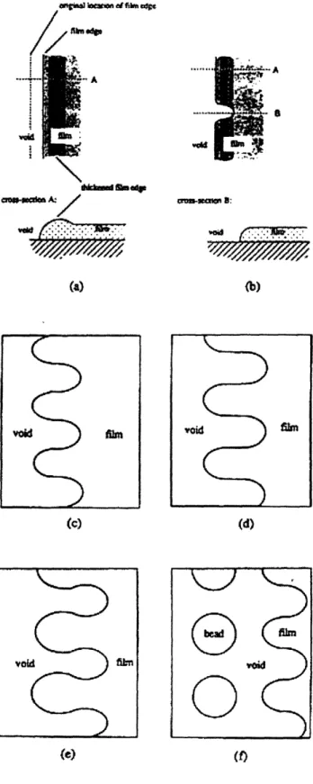
Grooving at the grain boundaries and triple junctions of a polycrystalline film is driven by the attempt to minimize the interfacial energy associated with these defects. The grooves can be large enough to reach the substrate. In this case, stable voids can form. Material is transferred from the area of the hole to its periphery by self-diffusion. The void grows by forming a lip with a cylindrical cross-section and a thickened edge (Fig. 2-3a). However, variations of the thickness are observed due to a Rayleigh-type instability of the rim caused by the uneven accumulation of material. According to Jiran and Thompson, as the void grows, it penetrates the thinner areas of the film faster (Fig. 2-3b) resulting in the edge instability mechanism summarized in Figures 2-3c to 2-3f [8]. The result is the decay of the continuous film into individual islands. Taking into account the fact that the void propagates faster through thin areas, the material removed from the substrate is expected to be deposited at stationary areas on either side of the penetrating void tip [8].
The above growth model was proposed by Jiran and Thompson in 1990 for Au thin films [8]. The thin films were deposited by electron beam evaporation and they were subsequent annealed. Annealing enhances atomic diffusion and the dewetting process can be observed in a reasonable amount of time.
/ mmrl _-W __~~~~ -:1 -z ~~~_- I l: rsirwwabnswrp fa) void (c)
Ca... .~ a*~
srmm-n~e~ B: WMl OWS-We"M 8:~ (b)i
(d)(e)
M(
Figure 2-3: a) The film edge is thickened after the transfer of material from the area of hole to its periphery. b) However, perturbations, which correspond to areas with smaller thickness, can grow faster than the rest of the film. c) - f) A series of perturbations which have penetrated the film result from a Rayleigh-type instability of the film edge and finally in the formation of
individuals beads [8]. 11 II .'.r II' i Ip~ II I A
2.2.3 Experimental Results and Conclusions
Jiran and Thompson modeled the void growth and predicted a constant growth rate and a thickness dependence of h-3, where h is the initial film thickness [8]. The thickness dependence explains the difference propagation velocities of the voids through the thinnest and the thickest areas of the film (Fig. 2-3). In a later study, their work was extended to include the stage of void nucleation in thin film agglomeration [9]. A Johnson - Mehl - Avrami (JMA) analysis was used to calculate the transformation curves for the process. The time required for surface grooves to penetrate the film was considered as the incubation time for the nucleation.
All the above research was conducted by the Materials for Micro- and Nano-Systems (MMNS) Group of the Department of Materials Science and Engineering (DMSE) at MIT during the early 90's. The agglomeration of Au thin films was examined. The above studies in combination with the studies made by different groups verify that dewetting of thin films is a process which can be utilized for the agglomeration of thin films of different materials [10-13].
2.3 Templated Dewetting of Metal Thin Films
2.3.1 Introduction
As it has been already discussed, we can force the self-assembly of nanoparticle arrays by depositing a thin film on a substrate and subsequently annealing it at high temperatures. The film will decompose into a collection of individual islands to decrease its energy. The process is initiated by grooving at grain boundaries or triple junctions and continues via a Rayleigh-type instability.
The self-assembly of nanoparticles by the dewetting process would be of particular interest if we could form ordered arrays of particles. Many potential applications of nanoparticles favor the formation of well-ordered nanoparticle arrays. The objective of this thesis is to discuss the fabrication of patterned magnetic media, plasmon waveguides and the catalytic growth of semiconducting nanowires and carbon nanotubes.
Following the studies by Jiran and Thompson, dewetting of a film on flat substrates results in the formation of nanoparticles with no ordering [8, 9]. This problem was resolved successfully by Giermann and Thompson [14, 15]. According to the novel technology developed by the MMNS Group of the DMSE at MIT, topographically modified substrates were used as templates for the formation of ordered nanoparticle arrays. Surfaces with di-periodic topography controlled the dewetting of thin films and provided a template for the ordering of the fabricated nanoparticles. Moreover, the nanoparticles are topographically confined on the surface. It is speculated that this might prevent coarsening during any high-temperature processing. There are additional advantages of the described technology, in terms of the orientation and the average size of the particles.
2.3.2 Experimental Steps
The first step of the templated dewetting process is the fabrication of the template. { 100} Si wafers were used as the substrates and interference lithography was employed as the patterning technique. The fabrication of the templates is explained in detail in table 2-1.
Table 2-1: Experimental steps for the fabrication of the dewetting templates with di-periodic topography [14, 15].
Templates with three different topographies were fabricated. The first topography had a period of 377 nm and a pit-to-mesa ratio equal to 1.5. The other two topographies had periods of 175 nm and pit-to-mesa ratios equal to 5.3 and 1.9 respectively.
After the fabrication of the substrate, the process continued with the deposition of thin films and their subsequent annealing. Au thin films of three different thicknesses were investigated (16, 21 and 32 nm). Thin films of every thickness were deposited on four different substrates: three topographically modified substrates and a flat Si substrate with a diffusion layer. Therefore, there were twelve different combinations of substrate's topography and initial thickness of deposited film. Table 2-2 summarizes the experimental steps of deposition and annealing.
Experimental
Template Fabrication
Steps
1. A masking layer of SiNx is grown on a { 100} Si wafer
2. A stack consisting of a XRHi-1 1 antireflective coating and an OKHA PS4 photoresist is spun onto the substrate
3. Two laser exposures of a 900 relative orientation are used to create a square array of holes (interference lithography)
4. Reactive ion etching is used (RIE) to transfer the pattern from the resist to the SiNX masking layer
5. The masked substrate is etched by being immersed in a KOH bath. Wet etching results in the formation of a periodic array of pits (which have the shape of inverted pyramids) bound by the { 111 } planes
6. The masking layer is removed
7. A thin diffusion barrier of SiO2 is grown on the surface by
Table 2-2: Experimental steps for thin-film deposition and annealing [14, 15].
2.3.3 Experimental Results
It was demonstrated that the templated dewetting process modifies the characteristics of the fabricated nanoparticles [14, 15]. In the following sections the ordering, size and crystallographic orientation of the particles will be correlated to the experimental parameters (substrate topography and initial thickness of the deposited film).
a) Ordering of nanoparticles: Results & Discussion
According to the results obtained by scanning electron microscopy, there were four different nanoparticle morphologies after the dewetting of the Au thin films [14, 15]:
I.
The particle arrays were random. This type of behavior was observed fordewetting on flat substrates. However, the same behavior was also observed when the 21 nm and 32 nm films were deposited on the 175 nm-period topography with a wide mesa (pit-to-mesa ratio equal to 1.9). It was clear that
Experimental
Film Deposition and Dewetting
Steps
1. Au thin films of thicknesses 16, 21 and 32 nm are deposited on all the topographically modified substrates (plus on a flat substrate) by electron beam evaporation
2. Dewetting is induced by annealing the substrates in air (2h at 850°C)
3. Scanning electron microscopy (SEM) is used to examine the morphology of the fabricated arrays
thin films of 21 nm and 32 nm thickness did not interact with the above topography.
II. There were multiple particles in every pit and larger particles on top of mesas. This type of behavior was observed when the 16 nm film interacted with the 377 nm-period and the 175 nm period with narrow mesa (pit-to-mesa ratio equal to 5.3).
III. There were ordered arrays of one nanoparticle per pit with large particles on
mesas. This was observed when the 21 nm and the 16 nm films were deposited
on the 377 nm-period topography and the 175 nm-period topography with a wide mesa respectively.
IV. There were ordered arrays of one nanoparticle per pit without extraneous and
undesired particles. This was the most desirable type of behavior and the goal of
the process. It was observed when the 21 nm thin film was deposited on substrates having a 175 nm-period topography with a narrow mesa. The average diameter of the fabricated nanoparticles was 120.7 nm ± 1.7 nm.
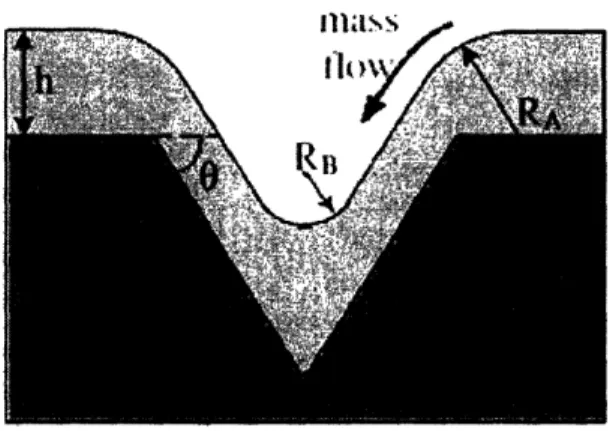
The experimental results can be explained by considering the geometry of the thin film during the initial stage of thermal annealing (Fig. 2-4). According to the analysis by Giermann and Thompson, the gold thin film has a positive curvature at point A and a negative curvature at point B [14]. The Gibbs-Thompson equation, Aj
= KyVm correlates the excess chemical potential At to the curvature K of the surface. Vm denotes the molar volume and y the surface energy. Because of the curvature variation, there is a positive excess chemical potential at the edge of the inverted pyramid and a negative A in the centre of the pyramid. The difference in the chemical potential is the driving force for atom diffusion towards the centre of each
fabricated hole. Atom diffusion will reduce the curvature at the edges and will increase the curvature in the centre of each hole. Eventually, the local curvature at the edges of the pyramid will become so small that it will result in a discontinuous film. As soon as the created grooves intercept the film-substrate interface, dewetting will continue according to the void-edge instability model, which was described by Jiran
and Thompson [8].
Figure 2-4: A cross-sectional view of the film and the substrate at the location of a pit during the
initial stage of thermal annealing. Mass flows towards the center of the pit in order to minimize the curvature variations at the surface of the thin film [141.
Type IV morphology can be justified by the above mechanism. In this case, the holes are so close to each other that the high curvature condition exists throughout the mesa width. This condition drives all the material off the mesas and into the holes, resulting in the most desired type of behavior.
This is not possible if the mesas are too wide. In such a case, the thin film is flat in the centre of the mesas and therefore there is no driving force for diffusing the whole amount of material into the centre of the pits. This material will remain on the mesas resulting in Type III morphology.
Type II morphology is observed when the gold film is very thin. Such a thin film may be discontinuous even before the annealing process, due to imperfections during the deposition technique. There can already be some grooves on the sidewalls or in the centre of each pyramid. When the film is annealed these random grooves result in the formation of nanoparticles in a random manner. Therefore, we observe
multiple particles per pit with no ordering.
When the initial film is too thick relative to the size of the pyramids, the thin film dewets as if it was deposited on a flat substrate ignoring the surface topography (Type I morphology). Very large film thickness results in very small curvature at the edge of the holes, which in turn yields a very small driving force for diffusion. Therefore,, there are no atoms diffusing towards the centre of the pits and the thin film dewets as if deposited on a flat surface.
b) Size of Nanoparticles: Results & Discussion
Another advantage of the described technology is that it results in the reduction of the average particle size in comparison to nanoparticles created on flat substrates. Results were confirmed by SEM and can be summarized as following [15]:
I. The average particle size decreased by about 75% in the case of the desired dewetting behavior, which yielded a single nanoparticle per hole.
II. The average particle size decreased by about 60% even when the fabricated particles did not interact with the substrate's topography.
The above phenomenon can be explained by the kinetics of Rayleigh instabilities. As already discussed, the dewetting process relies on Rayleigh-type
instabilities formed around the edge of the film. The topography of the substrate modifies the curvature of the receding film. The instabilities on a templated surface have a shorter length scale than the instabilities on a flat surface. Therefore, templated dewetting results in the creation of particles with smaller average diameters.
c) Crystallographic Orientation of Nanoparticles: Results & Discussion
The crystallographic orientation of nanoparticles was investigated using the pole figures obtained by the XRD technique [15]. When a polycrystalline Au thin film is deposited on a flat substrate, it develops a strong { 111 } texture as a result of the interfacial energy minimizing condition [16]. However, it will exhibit random in-plane orientation.
For particles created by dewetting of a film on a flat substrate, the above two observations are still valid. However, the results were very different for particles created by dewetting on a substrate with di-periodic topography. XRD pole figures provided clear evidence that the fabricated particles developed a {1001 crystallographic texture with uniform in plane orientation [15].
The fabricated particles have their <111> crystallographic directions normal to the sides of the pyramidal pits, due to the interfacial energy minimizing condition. The crystallographic texture of the thin films is determined by the normal to the plane of the substrate. Taking into account the angle of the pits (54.7°), it was easily determined that the direction normal to the substrate is of the <100> type [15]. This means that the fabricated particles have developed { 100 texture (instead of { 11 } on a flat surface).
In-plane orientation is speculated to be a further result of the fact that the fabricated particles have their <111> directions normal to the sides of the pits because
of the surface energy minimizing condition [15, 16]. In contrast to the deposition of a polycrystalline film on a flat substrate, in-plane orientation is well-determined by the geometry of the pits.
2.3.4 Advantages, Limitations and Challenges
According to the above experimental results, the templated dewetting process has many advantages. First of all, it results in the perfect ordering of the fabricated nanoparticle arrays. Secondly, the particles have uniform in-plane and out-of-plane orientation. Moreover, their average diameters are smaller than the corresponding values on a flat substrate. Finally, the topographical confinement of the nanoparticles might prevent coarsening or agglomeration during subsequent high temperature processing.
A disadvantage of the described technology is that its resolution is so far limited by the resolution of the patterning technique. Another limitation of the dewetting process is that perfect ordering can be only achieved by decay of a continuous thin film (patch or strip). Otherwise, the ordering of the fabricated particles will not follow the topographical features of the template. However, very thin films are expected to be discontinuous. Since the size of the dewetted particles is expected to be determined by the thickness of the deposited film, the above consideration poses a minimum limit on the size of the well-ordered fabricated nanoparticles.
Deposition of continuous thin films with very small thicknesses is a future challenge and plays a crucial role in the templated dewetting process. According to C.V. Thompson, film thickness at which coalescence occurs is about half of the average grain size at coalescence, assuming that the formed grain boundaries are
immobile [17]. Therefore, thin films with small average grain diameter, d, are desirable for the templated dewetting process, since they coalesce at a smaller thickness, h.
Polycrystalline thin films form through three successive steps. First, stable clusters are nucleated on a substrate. Secondly, these clusters grow by the adsorption of adatomns and finally they coalesce yielding a polycrystalline continuous film. C.V. Thompson modeled the above process and found that the average grain diameter at the point of coalescence can be approximated by the following equation [17]:
d 1. 3516 +1.203
i.
(Eq. 2.3)
5 denotes the width of a circular zone around a nucleated island in which any atom will diffuse to that island instead of desorbing or forming a new cluster. I is the nucleation rate and Go is a temperature-independent term, which is involved in the growth rate equation.
Go is directly proportional to the rate of deposition Fdep, while I is proportional to Fdep [117]. The critical cluster size n* is in the order of 2 in physical vapor deposition techniques [18]. Therefore, GJI decreases with increasing deposition rate. The width of the circular zone 6 is independent of Fdep. At low rates of deposition, the second tenm of equation 2.3 dominates and thus the average grain diameter decreases with increasing Fdep. At high rates of deposition, the first term of equation 2.3
dominates and d is independent of Fdep [17]. The results are summarized in Figure 2-5. High deposition rates are desirable in order to obtain a continuous thin film at a smaller thickness.
a
-- 1 a
In (R)
Figure 3-5: The average grain diameter, d, at coalescence vs. the deposition rate, R [17].
Except for the deposition rate, the average grain diameter depends on the substrate temperature, T. Higher temperatures enhance adatom diffusion to the nucleated clusters, resulting in grains with larger diameters at the point of coalescence. When the substrate temperature is lower, adatoms have lower mobilities and they tend to form new islands rather than diffuse to the previously nucleated clusters [18]. Therefore, the average grain diameter at the point of coalescence is
smaller. Figure 2-6 illustrates the dependence of d on the temperature of the
substrate. The natural logarithm of d is proportional to /T within regimes. The changes of the proportionality constant are due to the increase of n* with increasing temperature [17]. In conclusion, the minimum thickness of a continuous thin film is expected to decrease if we cool the substrate during the deposition process.
1/kT
Figure 2-6: The average grain diameter, d, at coalescence vs. the substrate temperature, T [17].
Moreover, the background pressure during evaporative or sputter deposition affects the average grain diameter and the film thickness at coalescence. At high pressures the deposited atoms lose energy through collisions with impurity atoms. Therefore., they have low mobilities resulting in a continuous film at a smaller thickness [18]. The same effect has an increase in the sputtering gas pressure [18].
The minimum thin film thickness depends on the melting temperature of the deposited material [18]. The melting point of a material reflects its binding energy. Strongly bound solids have a high melting temperature. In this case, it is more difficult for the deposited atoms to bind to an existing cluster. Therefore, thin films of materials with high melting temperatures tend to be continuous at a smaller thickness.
In conclusion, there are many modifications of the deposition process which can yield a continuous thin film with smaller thickness. Following these modifications, we can scale-down the templated dewetting process. A high deposition rate is desirable. In evaporative deposition, Fdep can be increased by increasing the source temperature, while in sputter deposition by applying a higher target-substrate bias. The substrate temperature should be maintained as low as possible during each deposition process. Moreover, a high background pressure is desirable, since it results
in adatorns with low mobilities. In the case of sputtering, sputtering gas with a high pressure contributes to the above result. Finally, thin films of materials with high melting temperatures are expected to result in a further decrease of the minimum film thickness.
2.3.5 Conclusions
The combination of dewetting with interference lithography provides us with a novel route for fabricating well-ordered nanoparticle arrays. The simplicity and low cost of the interference lithography coupled with the self-assembly characteristics of dewetting is very promising for large scale fabrication.
The objective of this thesis is to focus on the dewetting stage of the process and discuss the implementation of a few potential applications. Although emphasis will be given on the combination of dewetting with interference lithography, other patterning methods will be considered as well. Templated dewetting can be regarded as a novel method for transferring a pattern to the desired material. It can be therefore considered as a substitute for evaporation and lift-off, electrodeposition on patterned electrodes,, or etching.
The unique advantages of the templated dewetting process are very promising for a range of applications. The current limitations encountered at this early stage of explorations are expected to be overcome with continuous scientific research and future modifications of the process.
References
1. L. Rayleigh, Proc. London Math. Soc., 10, p. 4 (1879).
2. C. Trautmann, "Micro- and nanostructuring with energetic heavy-ions", website: www.nsc.emet.in/events/NSC WORKSHOP
3. F.A Nichols and W.W. Mullins, Trans. Metall. Soc. AIME, 233, p. 1840 (1965).
4. T. MUller, K.H. Heinig and B. Schmidt, Mat. Sci. Eng. C, 19, p. 209 (2002). 5. M.E. Toimil Molares, A.G. Balogh, T.W. Cornelius, R. Neumann and C.
Trautmann, Appl. Phys. Lett., 85, p. 5337 (2004). 6. W.W. Mullins, J. Appl. Phys., 30, p. 77 (1959).
7. D.J. Srolovitz and S.A. Safran, J. Appl. Phys., 60, p. 247 (1986). 8. E. Jiran and C.V. Thompson, J. Electron. Mater., 19, p. 1153 (1990). 9. E. Jiran and C.V. Thompson, Thin Solid Films, 208, p. 23 (1992).
10. D.J. Srolovitz and S.A. Safran, J. Appl. Phys., 60, p. 255 (1986). 11. D.C. Agrawal and R. Raj, Acta Metall., 37, p. 2035 (1989).
12. F.Y. Genin, W.W. Mullins and P. Wynblatt, Acta Metall. Mater., 40, p. 3239 (1992).
13. R. Dannenberg, E.A. Stach, J.R. Groza and B.J. Dresser, Thin Solid Films, 370), p. 54 (2000).
14. A.L. Giermann and C.V. Thompson, Mat. Res. Soc. Symp., 818, p. M3.3.1 (2004).
15. A.L. Giermann and C.V. Thompson, Appl. Phys. Lett., 86, p. 121903 (2005). 16. C.'V. Thompson, Annu. Rev. Mater. Sci., 30, p. 159 (2000).
18. C.V. Thompson, Massachusetts Institute of Technology, 3.48J Lecture Notes (2004).
PART II: ANALYSIS OF POTENTIAL
APPLICATIONS
3.
Plasmon Waveguides
3.1 Introduction
Conventional optical elements, such as dielectric waveguides, suffer from two serious limitations, which hinder their miniaturization. First of all, their size is limited by the diffraction limit of light [1]. This limit is about half the wavelength of the transmitted light. Therefore, for visible light this translates into a minimum element size of a few hundred nm. Another serious limitation is that complex guiding geometries, such as 90° corners, are not possible [2]. Plasmon waveguides are structures which can overcome the above limitations and guide electromagnetic energy in a coherent fashion via arrays of closely spaced metal nanoparticles. Their function relies on exploiting non-propagating fields of electromagnetic radiation [1].
Well-ordered nanoparticle arrays created by the technology of dewetting are potential candidates for the guidance of electromagnetic energy. The goal of this section is to discuss the challenges associated with the use of one-dimensional arrays of dewetted nanoparticles for fabricating plasmon waveguides.
3.2 Description
Metal nanoparticles interact with light at their resonance frequency due to the excitation of a collective motion of their conduction electrons. Energy is drawn into the particle because of its strong polarization [2]. The collective motion of the electrons is known as a surface plasmon polaritons (SPP). The intensity of SPPs is maximized at the surface of the nanoparticles and decays exponentially away from it. The evanescent fields of SPPs can exceed the optical excitation intensity by several orders of magnitude [1]. The particles should be much smaller than the wavelength of
light in order to achieve in-phase excitation of all the electrons. Nanoparticles in the order of 30 - 50 nm have been effectively used to guide electromagnetic energy [2]. Noble metals (Ag, Au, Cu) are of a particular interest, since their resonance frequencies lie in the visible range of light [2-4].
Electromagnetic energy is transferred along the nanoparticle chain in the form of plasmon oscillations taking advantage of the near-field electrodynamic interactions [1]. The first particle of the chain is irradiated by an external light field and gives rise to an SPP field with very high intensity near the illuminated particle. All the other particles get their plasma oscillation by coupling. The second particle is situated within the intense near-field created by the first particle and it picks up the optical excitation. Electromagnetic energy is transferred by the same way, all along the chain.
3.3 Optimum Dimensions of the Waveguide
3.3.1 Optimum size of the Nanoparticles
Because interest in plasmon waveguides is relatively recent, there has so far been no agreement on the optimum size of the used nanoparticles. However, the particles should fulfill two necessary conditions in order to allow efficient transfer of electromagnetic energy. They must be small enough, much smaller than the wavelength of the incident light, to achieve in-phase excitation of all the electrons, while at the same time they must be large enough to avoid enhanced damping due to surface scattering of the conduction electrons [2, 3].
It has been demonstrated that gold and silver nanoparticles with diameters between 30 and 50 nm satisfy the above conditions. Therefore, gold and silver
particles in the above size regime have been used as buildings blocks for the fabrication of plasmon waveguides [2-4].
3.3.2 Optimum Spacing of the Nanoparticles
The importance of regular particle spacing can be justified after a short overview of the damping mechanisms, which are encountered during the energy transfer along plasmon waveguides. Intensity loss can be due to three different reasons: inelastic surface scattering of the conduction electrons, radiation losses into the far-field and internal damping due to resistive heating. As already mentioned, the surface scattering effect can be minimized by working with nanoparticles having dimensions above a minimum limit. Moreover, radiation losses into the far-field are negligible because of the dominance of the near-field coupling mechanism. Therefore, the main reason for intensity loss is internal damping of the surface plasmon polaritons due to resistive heating. The dominance of the near-field coupling mechanism and its strong dependence on distance underline the importance of regular particle spacing [2, 3].
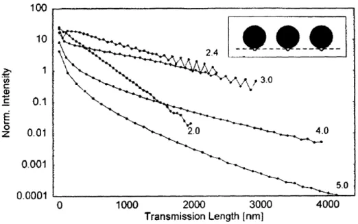
Quinten et al. have modeled the intensity decay vs. the transmission length for variations in the spacing of the particles [4]. Their analysis focused on Ag nanoparticles with 50 nm diameters. Maier et al. used the results obtained from the above modeling to propose two different methods for the fabrication of plasmon waveguides based on Au nanoparticles with diameters between 30 and 50 nm [2]. According to the simulation, the minimum transmission loss is observed for a center-to-center distance of 3r, where r is the radius of the nanoparticles. Quinten et al. predicted a signal attenuation coefficient of y=1.lx106 m-', which corresponds to 2.4 dB/500 nm. Brongersma et al. calculated analytically a value of 3 dB/500 nm, which
is in close agreement [3]. Intensity follows an exponential decay. Transmission loss is higher for particles which are more closely spaced. It reaches which is 2.3 times than at zero interparticle distance. The transmission loss is also higher for arrays with interparticle distances greater than 3r. In this case, the intensity decay is non-exponential.
-Iw
10 >1 1 u) C O. o Z 0.01 0.001 0.0001 0 1000 2000 3000 4000 Transmission Length [nm]Figure 3-1: The normalized intensity (I/Io) vs. the transmission length of the electromagnetic energy in a plasmon waveguide based on a regular array of Ag nanoparticles with 50 nm diameters. The numbers on each plotted line correspond to the different values of center-to-center spacing of the particles [4].
Figure 3-1 summarizes the results obtained from the numerical simulation of Quinten et al. [4]. The various plotted lines correspond to different center-to-center spacing (see inset of Figure 3-1) of the nanoparticles. The starting values of normalized intensity can be higher than I because of the resonantly enhanced field of the first nanoparticle. We can see that even for the optimum spacing, efficient propagation is limited to a few m at best. Therefore, rather than acting as waveguides in the conventional sense, which supports practically lossless light
propagation, nanoparticle arrays could be used as local devices focusing optical fields down to nanoscale volumes.
3.3.3 Other Considerations
The shape of the nanoparticles has an effect on the velocity of the energy propagation (group velocity). For example, since ellipsoids can be spaced closer together than spheres of the same volume, the group velocity along an array of ellipsoids is higher than for an array of spheres of equivalent volume [3]. Moreover, it is important that the fabrication method can produce nanoparticles of a narrow size and shape distribution, since position and width of the dipole resonance depend on these two factors [3]. Variations of the location and width of the dipole resonance can lead to inefficient transfer because of the strong distance dependence of the near-field coupling mechanism.
The choice of host matrix can also be important for various reasons. The term 'host matrix' refers to the ambient of nanoparticles deposited on a surface. A poor choice of a matrix can result in significant damping because the plasmons can couple to various degrees of freedom in the host. Moreover, by varying the refractive index (q) of the matrix, we can shift the resonance wavelength over several hundred nm. Finally, an increase in rI can decrease the coupling strength between the particles and thus reduce the group velocity [3]. The refractive indices of air and vacuum (ri=1.00029) and rq=1.0 correspondingly) are expected to work well for the fabrication of plasmon waveguides [2, 3].
3.4 Dewvetting of Nanowires for the Fabrication of Plasmon Waveguides
The process of dewetting must be combined with a patterning technology (e.g. lithography) in order to produce nanoparticle arrays necessary for the fabrication of plasmon waveguides. We need a patterning technology capable of fabricating one-dimensional structures with feature sizes determined by the capillary instability [5-8].
The simplest plasmon waveguide could be fabricated by the dewetting of a single line. However, in order to fabricate a device based on waveguides, we need to have a complicated waveguide pattern. Interference lithography cannot be a candidate for patterning, since it is not capable of patterning complex waveguide patterns required for the fabrication of a completed circuit. Dewetting should therefore be combined with electron beam lithography, X-Ray lithography or any other kind of patterning technology capable of producing one-dimensional, non-periodic structures, which can dewet to form nanoparticles with sizes in the range of 30 to 50 nm.
For the analysis of this section we will consider the simplest case, which is the dewetting of a nanowire deposited on a substrate. This is a different type of templated dewetting technology than that described in section 2.3. There is no substrate with topographical features. The dewetting process is instead confined in a one-dimensional track patterned using a lithographic technique. We will base our analysis on the results determined by Nichols for the instability of infinite cylinders of solid materials, which are free from any surface contact [8]. These results were summarized in section 2.1 of this thesis. It should be noted again that we are ignoring the effect of the substrate on determining the fastest growing wavelength of perturbations.
A serious disadvantage of the dewetting technology for the fabrication of plasmon waveguides arises from the consideration of the average spacing determined by the capillary instability [5-8]. Following the analysis presented in section 2.1, and
considering the above-stated assumption, we can calculate the diameter and spacing of the nanoparticles fabricated by the dewetting of a nanowire. The average diameter of the fabricated particles and the average center-to-center spacing are related to the initial wire radius R by the previously stated equations 2.1 and 2.2.
According to equation 2.2, we could obtain dewetted particles in the 30-50 nm regime if we could pattern one-dimensional structures with initial radii between 8 and 13 nm. After a straightforward calculation (substituting R with d/3.78 in equation 2.1), we find that the average center-to-center spacing of the fabricated nanoparticles is equal to 4.7r, where r is their diameter. According to figure 3-1, plasmon waveguides with such a large spacing will suffer from huge intensity losses even if the transmission length is as small as a few hundred nanometers. Such an array would be only suitable for short-range optical addressing of individual nanoparticles. Dewetting can produce nanoparticles with regular spacing and narrow size and shape distributions; however the disadvantage of the large interparticle distances predominates over the advantage of the achievable uniformity.
3.5 Conclusions
The dewetting process of one-dimensional structures for the fabrication of plasmon waveguides suffers from one major disadvantage. The dewetted nanoparticles are more widely spaced (4.7r) than the optimum distance (3r). Therefore, intensity loss is increased and the process is considered as a bad candidate for waveguide fabrication.
Many different techniques have been proposed for the construction of nanoparticle waveguides. Maier et al. have demonstrated two different techniques [2]. The first method is a combination of electron beam lithography and lift-off, while the
second relies on the manipulation of randomly deposited nanoparticles using an AFM tip. A novel self-assembly technique for the fabrication of plasmon waveguides was proposed by McMillan et al. and relies on the use of nanoscale templates made of chaperonin proteins [9].
It should be noted that the technology of plasmon waveguides is still at an embryonic stage and many questions remain unanswered. All investigations of the optical properties of the waveguides have so far been confined to collective excitations [10-12]. No direct measurement of electromagnetic energy transport along the nanoparticle chains has yet been made.
References
1. J.R. Krenn, Nature Mater., 2, p. 210 (2003).
2. S.A. Maier, M.L. Brongersma, P.G. Kik, S. Meltzer, Ari A.G. Requicha and H..A. Atwater, Adv. Mater., 13, p. 1501 (2001).
3. M.L. Brongersma, J.W. Hartman and H.A. Atwater, Phys. Rev. B, 62, p. R :16356 (2000).
4. M. Quinten, A. Leitner, J.R. Krenn and F.R. Ausssenegg, Opt. Lett., 23, p. 1331 (1998).
5. T. MUller, K.-H. Heinig and B. Schmidt, Mat. Sci. Eng. C, 19, p. 209 (2002). 6. M.E. Toimil Molares, A.G. Balogh, T.W. Cornelius, R. Neumann and C.
Tr;autmann, Appl. Phys. Lett., 85, p. 5337 (2004). 7. L. Rayleigh, Proc. London Math. Soc., 10, p. 4 (1879).
8. F.A. Nichols and W.W. Mullins, Trans. Metall. Soc. AIME, 233, p. 1840 (1965).
9. R.A. McMillan, C.D. Paavola, J. Howard, S. L. Chan, N. J. Zaluzec and J. I:). Trent, Nature Mater., 1, p. 247 (2002).
10. J.R. Krenn, A. Dereux, J.C. Weeber, E. Bourillot, J.P. Goudonnet, G. Schider, W. Gotschy, A. Leitner, F.R. Aussenegg and C. Girard, Phys. Rev. Lett., 82, p. 2590 (1999).
11. S.A. Maier, M.L. Brongersma, P.G. Kik and H.A. Atwater, Phys. Rev. B, 65, p. 1.93408 (2002).
4.
Patterned Magnetic Media
4.1 Magnetic Media Evolution
4.1.1 Conventional Magnetic Media - Definition & Limitations
Magnetic data storage is widely used in applications like audio tapes, video cassette recorders, computer hard disks, floppy disks and credit cards. Hard disks and floppy disks are also referred as rigid magnetic media to distinguish them from the magnetic tapes. Nowadays, magnetic hard disk recording is the most widely used of all the magnetic storage technologies. Hard disk recording remains the primary and most economical means of data storage in today's computer. Advances in the speed of a microprocessor are always accompanied by advances in storage capacity, contributing to the enhancement of the capabilities of modern computers.
ktoioe coil actuator
:Hed
latters
..- i , JE 3 \
Z cf s':.
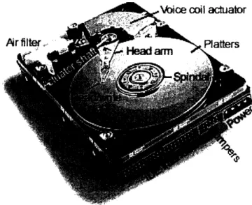
Figure 4-1: Top-view of the basic parts of a conventional Hard Disk Drive (HDD). A HDD can contain one or more magnetic hard disks (platters) [1].
A conventional magnetic medium (e.g. a hard disk) consists of four layers; a substrate, an underlayer, a magnetic film where the data is stored, and a protective overcoat. The magnetic thin film is usually a polycrystalline alloy of cobalt, chromium and platinum (or tantalum), which is sputtered at elevated temperatures [2, 3]. The above alloy is used due to its high magnetic anisotropy. During magnetic recording, an external magnetic field is applied by the writing head. Data is stored in concentric circles, which are called 'tracks'. Small areas of the track (bits) are magnetized parallel or antiparallel to the track direction (Fig. 4-3). Since the magnetization of the recording bits lies in the plane of the film, the prevailing technology of thin film media is also known as longitudinal recording. During the reading process, the reading head detects magnetic fields coming from places where the magnetization changes. If a magnetic field is present, stored data is interpreted as ' 1 '; if a magnetic field is absent, it is interpreted as '0' [2, 4]. In order to increase the amount of information the drive can store, most HDDs have multiple hard disks (platters) and magnetic heads (Fig. 4-1).
Each bit of the polycrystalline thin film consists of many grains, which are created during the deposition process. The grains behave as tiny magnets whose magnetization can be flipped by the writing head during the data writing process. In conventional magnetic media, the overall signal-to-noise ratio (SNR), is expected to be determined by the transition noise originating from irregularities in the magnetization transitions at the bit boundaries (Fig. 4-2). These irregularities become very sharp if the bits of the polycrystalline thin film contain few grains. Therefore, the number of grains, N, within a single bit determines the signal-to-noise ratio of the medium. It has been demonstrated that SNR is proportional to N1/2 [3, 8]. Thus, as the number of bits and consequently the density of the medium increase, an acceptable
SNR can be only achieved by maintaining a large number of grains within each bit. To keep the noise small enough for reliable data detection, roughly 50-100 grains are needed per bit [3]. To achieve a reduction of the bit size, we should therefore decrease the average grain size.
rain
Net magnetization of film
Magnetization transition
Figure 4-2: The magnetized grains of a conventional thin film medium. Magnetic noise arises because of the magnetization transitions between two adjacent bits [2].
However, when the grains become very small their magnetization is subject to thermal fluctuations. This phenomenon is well known as the superparamagnetic limit and can be quantified by the ratio KV/kT [2, 5]. K denotes the net magnetic anisotropy of the grain, k the Boltzmann constant, V the grain volume and T is the temperature of operation. This stability criterion is valid for magnetic media with uniaxial magnetic anisotropy. For a thermally stable medium, the accepted values of the above ratio are on the order of 60 [2, 3, 50, 51]. For longitudinal thin film media, the superparamagnetic effect is expected to occur at densities of 6 - 15 Gbit/cm2[2].
To overcome the limit determined by the stability ratio, we should either decrease the temperature of operation, or increase the anisotropy of the medium. Temperature could be theoretically decreased down to cryogenic values but operation at such small temperatures would be a complicated process for current magnetic media and electronic devices. Moreover, an increase in K would result in an increase in the coercivity of the medium, which would in turn require stronger writing fields. Therefore, a paradigm shift is required to overcome the limitations of longitudinal
thin film media.
4.1.2 Patterned Magnetic Media - Definition & Advantages
Two different approaches, which could overcome the thermal limitations, have been demonstrated. Perpendicular recording aligns the magnetization of the bits vertically, perpendicular to the disk, which allows additional room on a disk to pack more data; thus, enabling higher storage capacities. The demagnetizing fields the bits exert upon each other are smaller than in longitudinal recording. Therefore, perpendicular media enjoy five times greater thermal stability limits than longitudinal media, where the bits are aligned horizontally, parallel to the surface of the disk. It has been estimated that perpendicular media can reach up to 150 Gb/cm2capacities [2].
The: fabrication and use of patterned magnetic media is an even more revolutionary approach. The term patterned media refers to media for which each bit consists of' an isolated piece or grain of magnetic material. They are arranged periodically to be synchronized with a signal channel, which is an external magnetic field. The periodic arrangement can be achieved using high-resolution lithography or a templated self-assembly technique. It should be noted that a magnetic element (bit) is a single magnetic domain. It could be formed either by one grain or by several
grains, whose magnetization is dependent on the magnetization of surrounding grains. These grains are called 'exchange coupled' grains. On the other hand, thin film media consists of a collection of grains, which behave as tiny magnets with independent magnetization (random decoupled grains) [3].
Patterned media have two important advantages over conventional thin film media. First of all, they eliminate the noise associated with multigrain bits and magnetization transitions (Fig. 4-2, Fig. 4-3), since the magnetic bits are defined by the physical patterning and not by the grain boundaries between two oppositely magnetized regions. Moreover, the thermal stability ratio, KV/kT, refers to the volume and the anisotropy of the entire element and not to individual grains. Since we do not longer need on the order of 100 grains per bit, but just one single grain-sized switching volume, the bit size can be significantly smaller. Density can be increased by roughly two orders magnitude compared to conventional recording media. Patterned media are expected to give storage densities exceeding 150 Gb/cm2[2, 7].
Conventional hAhjtraqin Meia% . ^ 0 nmagnetization o ma17 t!ation trajlrvuIl bitclf recorde d i o:.ig o dadtat a 1k garns data or ' ' i 1 ' 0 o1 il
coaksc
Vx;r'
I I -II /pU\.. \
IL 'i&~~Figure 4-3:: Tracks and bits in a conventional magnetic thin film medium and in a novel patterned medium. The magnetization transitions between the bits of a patterned medium are avoided because the bits are defined by the patterning process [3].
Nanoparticles fabricated by the templated dewetting process of a magnetic thin film are potential candidates for the fabrication of patterned magnetic media. We will discuss the feasibility of this application by identifying the relevant limitations and challenges of templated dewetting. The desired dimensions and crystallographic orientation of the magnetic nanoparticles are determined by the limitations of patterned media and the magnetic anisotropy theory. Therefore, before we discuss the advantages and disadvantages of the dewetting technology for the fabrication of magnetic media, we should first identify the importance of magnetic anisotropy and the inherent limitations of the patterned media.
···-··y-··
41w!''
..i-: .m;mnpn
![Figure 2-2: Decay of an infinite liquid cylinder into a collection of droplets via a Rayleigh instability [2].](https://thumb-eu.123doks.com/thumbv2/123doknet/14173718.474951/15.918.363.548.782.1024/figure-decay-infinite-cylinder-collection-droplets-rayleigh-instability.webp)
![Table 2-1: Experimental steps for the fabrication of the dewetting templates with di- di-periodic topography [14, 15].](https://thumb-eu.123doks.com/thumbv2/123doknet/14173718.474951/22.918.151.762.97.577/table-experimental-steps-fabrication-dewetting-templates-periodic-topography.webp)
![Table 2-2: Experimental steps for thin-film deposition and annealing [14, 15].](https://thumb-eu.123doks.com/thumbv2/123doknet/14173718.474951/23.918.154.753.99.354/table-experimental-steps-film-deposition-annealing.webp)
![Figure 3-5: The average grain diameter, d, at coalescence vs. the deposition rate, R [17].](https://thumb-eu.123doks.com/thumbv2/123doknet/14173718.474951/30.918.329.576.109.365/figure-average-grain-diameter-coalescence-vs-deposition-rate.webp)
![Figure 2-6: The average grain diameter, d, at coalescence vs. the substrate temperature, T [17].](https://thumb-eu.123doks.com/thumbv2/123doknet/14173718.474951/31.918.330.556.99.337/figure-average-grain-diameter-coalescence-vs-substrate-temperature.webp)