-9
Architectural Implications of Bit-level
Computation in Communication Applications
by
David Wentzlaff
B.S.E.E., University of Illinois at Urbana-Champaign 2000
Submitted to the Department of Electrical Engineering and Computer
Science
in partial fulfillment of the requirements for the degree of
Master of Science in Electrical Engineering and Computer Science
BARKER
at the
MASSACHUSETTS INSTITUTEOF TECHNOLOGY
MASSACHUSETTS INSTITUTE OF TECHNOLOGY!
NOV 18 2002
September 2002
LIBRARIES
©
Massachusetts Institute of Technology 2002. All rights reserved.
A uthor ...
...
Department of Electrical Engineeing and Computer Science
A4
September 3, 2002
Certified by...
Professor of Electrical Engineering
Anant Agarwal
and Computer Science
Thesis Supervisor
Accepted by...
....
Arthur C. Smith
Chairman, Department Committee on Graduate Students
Architectural Implications of Bit-level Computation in
Communication Applications
by
David Wentzlaff
Submitted to the Department of Electrical Engineering and Computer Science on September 3, 2002, in partial fulfillment of the
requirements for the degree of
Master of Science in Electrical Engineering and Computer Science
Abstract
In this thesis, I explore a sub domain of computing, bit-level communication
process-ing, which has traditionally only been implemented in custom hardware. Computing
trends have shown that application domains previously implemented only in special purpose hardware are being moved into software on general purpose processors. If we assume that this trend continues, we must as computer architects reevaluate and propose new superior architectures for current and future application mixes. I believe that bit-level communication processing will be an important application area in the future and hence in this thesis I study several applications from this domain and how they map onto current computational architectures including microprocessors, tiled architectures, FPGAs, and ASICs. Unfortunately none of these architectures is able to efficiently handle bit-level communication processing along with general purpose computing. Therefore I propose a new architecture better suited to this task.
Thesis Supervisor: Anant Agarwal
Acknowledgments
I would like to thank Anant Agarwal for advising this thesis and imparting on me
words of wisdom. Chris Batten was a great sounding board for my ideas and he helped me collect my thoughts before I started writing. I would like to thank Matthew Frank for helping me with the mechanics of how to write a thesis. I thank Jeffrey Cook and Douglas Armstrong who helped me sort my thoughts early on and reviewed drafts of this thesis. Jason E. Miller lent his photographic expertise by taking photos for my appendix. Walter Lee and Michael B. Taylor have been understanding officemates throughout this thesis and have survived my general crankiness over the summer of 2002. Mom and Dad have given me nothing but support through this thesis and my academic journey. Lastly I would like to thank DARPA, NSF, and Project Oxygen for funding this research.
Contents
1 Introduction 13 1.1 Application Domain . . . . 14 1.2 Approach ... .. ... 16 2 Related Work 19 2.1 Architecture . . . . 19 2.2 Software Circuits . . . . 20 3 Methodology 21 3.1 M etrics . . . . 21 3.2 T argets . . . . 23 3.2.1 IBM SA-27E . . . . 23 3.2.2 X ilinx . . . . 25 3.2.3 Pentium . . . . 27 3.2.4 R aw . . . . 29 4 Applications 33 4.1 802.11a Convolutional Encoder . . . . 334.1.1 Background . . . . 33
4.1.2 Implementations . . . . 37
4.2 8b/10b Block Encoder . . . . 43
4.2.1 Background . . . . 43
5 Results and Analysis 5.1 Results ...
5.1.1 802.11a Convolutional Encoder .
5.1.2 8b/10b Block Encoder . . . . 5.2 A nalysis . . . . 6 Architecture 6.1 Architecture Overview . . . . 6.2 Yoctoengines . . . . 6.3 Evaluation . . . . 6.4 Future Work . . . . 7 Conclusion
A Calculating the Area of a Xilinx
A.1 Cracking the Chip Open . ...
A.2 Measuring the Die ...
A.3 Pressing My Luck . . . .
Virtex II . . . . . . . . . . . . 49 49 49 53 56 59 59 63 67 68 71 73 74 78 80
List of Figures
1-1 An Example Wireless System
3-1 3-2 3-3 3-4 4-1 4-2 4-3 4-4 4-5 4-6 4-7 4-8 4-9 4-10 4-11 4-12 4-13 4-14 4-15
The IBM SA-27E ASIC Tool Flow . . . . Simplified Virtex II Slice Without Carry Logic . . . . Xilinx Virtex II Tool Flow . . . . Raw Tool Flow . . . . 802.11a Block Diagram . . . . 802.11a PHY Expanded View taken from [18] . . . . Generalized Convolutional Encoder . . . . 802.11a Rate 1/2 Convolutional Encoder . . . . Convolutional Encoders with Feedback . . . . Convolutional Encoders with Tight Feedback . . . . Inner-Loop for Pentium reference 802.11a Implementation . Inner-Loop for Pentium lookup table 802.11a Implementation Inner-Loop for Raw lookup table 802.11a Implementation . . Inner-Loop for Raw POPCOUNT 802.11a Implementation . Mapping of the distributed 802.11a convolutional encoder on 16
tiles . . . . Overview of the 8b/10b encoder taken from [30] . . . .
8b/10b encoder pipelined . . . .
Inner-Loop for Pentium lookup table 8b/10b Implementation . . Inner-Loop for Raw lookup table 8b/10b Implementation . . . .
15 . . . . . 24 . . . . . 26 . . . . . 28 . . . . . 30 . . . . . 34 . . . . . 35 . . . . . 36 . . . . . 37 . . . . . 38 . . . . . 38 . . . . . 39 . . . . . 40 . . . . . 41 . . . . . 42 Raw 42 45 46 46 47
5-1 802.11a Encoding Performance (MHz.) . . . . 51
5-2 802.11a Encoding Performance Per Area (MHz./mm2.) . . . . 52
5-3 8b/10b Encoding Performance (MHz.) . . . . 54
5-4 8b/10b Encoding Performance Per Area (MHz./mm2.) . . . . 55
6-1 The 16 Tile Raw Prototype Microprocessor with Enlargement of a Tile 60 6-2 Interfacing of the Yoctoengine Array to the Main Processor and Switch 62 6-3 Four Yoctoengines with Wiring and Switch Matrices . . . . 64
6-4 The Internal Workings of a Yoctoengine . . . . 65
A-1 Aren't Chip Carriers Fun . . . . 74
A-2 Four Virtex II XC2V40 Chips . . . . 75
A-3 Look at all Those Solder Bumps . . . . 75
A-4 The Two Parts of the Package . . . . 76
A-5 Top Portion of the Package, the Light Green Area is the Back Side of the D ie . . . . 77
A-6 Removing the FR4 from the Back Side of the Die . . . . 78
A-7 Measuring the Die Size with Calipers . . . . 79
List of Tables
3.1 Summary of Semiconductor Process Specifications . . . . 22
5.1 802.11a Convolutional Encoder Results . . . . 50
5.2 8b/10b Encoder Results . . . . 54
Chapter 1
Introduction
Recent trends in computer systems have been to move applications that were previ-ously only implemented in hardware into software on microprocessors. This has been motivated by several factors. Firstly microprocessor performance has been steadily increasing over time. This has allowed more and more applications that previously could only be done in ASICs and special purpose hardware, due to their large com-putation requirements, to be done in software on microprocessors. Also, added ad-vantages such as decreased development time, ease of programming, the ability to change the computation in the field, and the economies of scale due to the reuse of the same microprocessor for many applications have influenced this change.
If we believe that this trend will continue, then in the future we will have one computational fabric that will need to do the work that is currently done by all of the chips inside of a modern computer. Thus we will need to pull all of the computation that is currently being done inside of helper chips onto our microprocessors. We have already seen this being done in current computer systems with the advent of all software modems.
Two consequences follow from the desire to implement all parts of a computer system in one computational fabric. First, the computational requirements of this one computational fabric are now much higher. Second, the mix of computation that it will be doing is significantly different from applications that current day micro-processors are optimized for. Thus if we want to build future architectures that can
handle this new application mix, we need to develop architectural mechanisms that efficiently handle conventional applications, SpecInt and SpecFP [8], multimedia ap-plications, which have been the focus of significant research recently, and the before mentioned applications which we will call software circuits.
In modern computer systems most of the helper chips are there to communicate with different devices and mediums. Examples include sound cards, Ethernet cards, wireless communication cards, memory controllers and I/O protocols such as SCSI and Firewire. This research work will focus on the subset of software circuits for communication systems, examples being Ethernet cards (802.3) and wireless commu-nication cards (802.11a, 802.11b). Commucommu-nication systems are chosen as a starting point for this research for two reasons. One, it is a significant fraction of the software circuits domain. Secondly, if communication bandwidth is to continue to grow as is foreseen, the computation needed to handle it will become a significant portion of our future processing power. This is mostly due to the fact that communication band-width is on a steep exponentially increasing curve. This research will further focus on bit-level computation contained in communication processing. Fine grain bit-level computation is an interesting sub-area of communications processing, because unlike much of the rest of communications processing, it is not easily parallelizable on word oriented systems because very fine grain, bit-level, communication is needed. Exam-ples of this type of computation include error-correcting codes, convolutional codes, framers, and source coding.
1.1
Application Domain
In this thesis, I investigate several kernels of communications applications that ex-hibit non-aligned, bit-level, computation that is not easily parallelized on word-oriented parallel architectures such as Raw [29, 26]. Figure 1-1 shows a block diagram of an example software radio wireless communication system. The left dotted box contains computation which transforms samples from an analog to digital converter into a demodulated and decoded bit-stream. This box typically does signal
process-Filtering Error Correction Protocol Processing
ADC Demodulation Framing Decapsulation
Application
Modulation Error Correction Protocol Processing
* ACEncoding Encapsulation
Samples Bits Frames
to to to
Bits Frames Frames/Packets
FFT Coders Route Lookups
FIR Decoders IP header generation
Framers Packet Encryption
Figure 1-1: An Example Wireless System
ing on samples of data. In signal processing, the data is formatted in either a fixed point or floating point format, and thus can be efficiently operated on by a word-oriented computer. In the right most dotted box, protocol processing takes place. This transforms frames received from a framer into higher level protocols. An ex-ample of this is transforming Ethernet frames into IP packets and then doing an IP checksum check. Once again frames and IP packets can be packed into words without too much inefficiency. This thesis focuses on the middle dotted box in the figure. It is interesting to see that the left and right boxes contain word-oriented computation, but the notion of word-aligned data disappears in this box. This middle processing step takes the bit-stream from the demodulation step and operates on the bits to remove encoding and error correction. This processing is characterized by the lack of aligned data and is essentially a transformation from one amorphous bit-stream to a different bit-stream. This thesis will focus on this unaligned bit domain. We will call this application domain bit-level communication processing.
on parallel architectures is because the parallelism that exists in these applications is inside of one word. Unfortunately for current parallel architectures composed of word-oriented processors, operations that exist on word-oriented processors are not well suited for exploiting unstructured parallelism inside of a word.
Two possible solutions exist to try to exploit this parallelism in normal parallel architectures yet they fall short. One approach is to use a whole word to represent
a bit and thus a word-oriented parallel architecture can be used to exploit paral-lelism. Unfortunately this type of mapping is severely inefficient, due to the fact that a whole word is being used to represent a bit, and if any of the computation has communication, the communication delay will be high because the large word-oriented functional units require more space than bit-level functional units. Thus they physically have to be located further apart. Finally, if all of these problems are solved, there are still problems if sequential dependencies exist in the computation.
If the higher communication latency is on the critical path of the computation, the
throughput of the application will be lowered. Thus for these reasons, simply scaling up the Raw architecture is not appropriate to speedup these applications.
The second possible parallel architecture that could exploit parallelism in these applications is sub-word SIMD architectures such as MMX [22]. Unfortunately, if applications exhibit intra-word communication, these architectures are not suited because they are set up to parallelly operate on and not communicate between sub-words.
1.2
Approach
To investigate these applications I feel that first we need a proper characterization of these applications on current architectures. To that end, I coded up two characteristic applications in 'C', Verilog, and assembly for conventional architectures (x86), Raw architectures, the IBM ASIC flow, and FPGAs and compared relative speed and area tradeoffs between these different approaches. This empirical study has allowed me quantify the differences between the architectures. From these results I was able to
quantitatively determine that tiled architectures do not efficiently use silicon area for
bit-level communication processing. Lastly I discuss how to augment the Raw tiled
architecture with an array of finer grain computational elements. Such an architecture is more capable of handling both general purpose computation efficiently and bit-level
Chapter 2
Related Work
2.1
Architecture
Previous projects have investigated what architectures are good substrates for bit-level computation in general. Traditionally many of these applications have been been implemented in FPGAs. Examples of the most advanced commercial FPGAs can be seen in Xilinx's product line of Virtex-E and Virtex-II FPGAs [33, 34]. Unfortunately for FPGAs, the difficulty of programming and inability of virtualization have stopped them from becoming a general purpose computing platform. One attempt made to use FPGAs for general purpose computing was made by Babb in [2]. In Babb's thesis, he investigates how to compile 'C' programs to FPGAs directly using his compiler named deepC. Unfortunately, due to the fact that FPGAs are not easily virtualized, large programs cannot currently be compiled with deepC.
Other approaches that try to excel at bit-level computation, but still be able to do general purpose computation include FPGA-processor hybrids. They range widely on whether they are closer to FPGAs or modern day microprocessors. Garp [6, 7] for example is a project at The University of California Berkeley that mixes a processor along with a FPGA core on the same die. In Garp, both the FPGA and the processor can share data via a register mapped communication scheme. Other architectures put reconfigurable units as slave functional units to a microprocessor. Examples of this type of architecture include PRISC [25] and Chimaera [13].
The PipeRench processor [11] is a larger departure from a standard microprocessor with a FPGA put next to it. PipeRench contains long rows of flip-flops with lookup tables in between them. In this respect it is very similar to a FPGA but has the added bonus that it has a reconfigurable data-path that can be changed very quickly on a per-row, per-cycle basis. Thus it is able to be virtualized and allows larger programs to be implemented on it.
A different approach to getting speedup on bit-level computations is by simply
adding the exact operations that your application set needs to a general purpose mi-croprocessor. In this way you build special purpose computing engines. One example of this is the CryptoManiac [31, 5]. The CryptoManiac is a processor designed to run cryptographic applications. To facilitate these applications, the CryptoManiac supports operations common in cryptographic applications. Therefore if it is found that there are only a few extra instructions needed to efficiently support bit-level computation, a specialized processor may be the correct alternative.
2.2
Software Circuits
Other projects have investigated implementing communication algorithms that previ-ously have only been done in hardware on general purpose computers. One example of this can be seen in the SpectrumWare project [27]. In the SpectrumWare project, participants implemented many signal processing applications previously only done in analog circuitry for the purpose of implementing different types of software ra-dios. This project introduced an important concept for software radios, temporal decoupling. Temporal decoupling allows buffers to be placed between different por-tions of the computation thus increasing the flexibility of scheduling signal processing applications.
Chapter 3
Methodology
One of the greatest challenges of this project was simply finding a way to objectively compare very disparate computing platforms which range from a blank slate of silicon all the way up to a state of the art out-of-order superscalar microprocessor. This section describes the architectures that were mapped to, how they were mapped to, how the metrics used to compare them were derived, and what approximations were made in this study.
3.1
Metrics
The first step in objectively comparing architectures is to choose targets that very nearly reflect each other in terms of semiconductor process. While it is possible to scale between different semiconductor feature sizes, not everything simply scales. Characteristics that do not scale include wire delay and the proportions of gate sizes. Thus a nominal feature size of 0.15pm drawn was chosen. All of the targets chosen with the exception of the Pentium 4 (0.13pm.) and Pentium 3 (0.18pm.) are fabri-cated with this feature size. Because everything is essentially on the same feature size this thesis will use area in mm2. as one of its primary metrics. One assumption that
is made in this study is that voltage does not significantly change performance of a circuit. While the targets are essentially all on the same process, they do have dif-ferences when it comes to nominal operational voltages. Table 3.1 shows the process
Target Foundry Ldrawn Leffective Nominal Layers Type
(pm.) (jm.) Voltage of of
(Volts) Metal Metal
IBM SA-27E ASIC IBM 0.15 0.11 1.8 6 Cu
Xilinx Virtex II UMC 0.15 0.12 1.5 8 Al
Intel Pentium 4 Intel 0.13 0.07 1.75 6 Cu
Northwood 2.2GHz.
Intel Pentium 3 Intel 0.18 Unknown 1.7 6 Al
Coppermine 993MHz.
Raw IBM 0.15 0.11 1.8 6 Cu
300MHz. I
Table 3.1: Summary of Semiconductor Process Specifications
parameters for the differing targets used in this thesis.
To objectively compare the performance of the differing platforms the simple metric of frequency was used. The applications chosen have clearly defined rates of operation which are used as a performance metric. For the targets that are software running on an processor, the testing of the applications was done over a randomly generated input of several thousand samples. This was done to mitigate any variations that result from differing paths through the program. This method should give an average case performance result. In the hardware designs, performance was measured
by looking at the worse case combinational delay of the built circuit. In order for
the the delay to the pins and other edge effects from accidentally being factored into the hardware timing numbers, registers were placed at the beginning and end of the design under test. These isolation registers were included in the area calculations for the hardware implementations. Lastly the latency through any of the software or hardware designs was not measured and deemed unimportant because all of the designs have relatively low latency and the applications are bandwidth sensitive not latency sensitive.
3.2
Targets
3.2.1
IBM SA-27E
Overview
The IBM SA-27E ASIC process is a standard cell based ASIC flow. It has a drawn transistor size of 0.15pm and 6 layers of copper interconnect [16]. It was chosen primarily to show what the best case that can be done when directly implementing the applications in hardware looks like. While using a standard cell approach is not as optimal as a full-custom realization of the circuits, it is probably characteristic of what would be done if actually implementing the applications, because full-custom implementations are rarely done due to time to market constraints. Conveniently this tool flow was available for this thesis because the Raw research group is using this target for the Raw microprocessor.
Tool Flow
For this target, the applications were written in the Verilog Hardware Description Language (HDL). Verilog is a HDL which has similar syntax to 'C' and allows one to behaviorally and structurally describe circuits. The same code base was shared between this target and the Xilinx target. The applications were written in a mixture of behavioral and structural Verilog.
To transform the Verilog code into actual logic gates a Verilog synthesizer is needed. Synopsys's Design Compiler 2 was utilized. Figure 3-1 shows the flow used. Verilog with VPP 1 macros is first processed into plain Verilog code. Next, if the circuit is to be simulated, the Verilog is passed onto Synopsys's VCS Verilog simulator. If synthesis is desired, the Verilog along with the IBM SA-27E technology libraries are fed into Synopsys's Design Compiler 2 (DC2). Design Compiler 2 compiles, analyzes, and optimizes the output gates. A design database is the output of DC2 along with area and timing reports. To get optimal timing, the clock speed was slowly 'VPP is a Verilog Pre-Processor which expands the language to include auto-generating Verilog code, much in the same way that CPP allows for macro expansion in 'C'.
Simulation
Verilog (with Macros)
VPP Technology Library vCS Design Area DB Report Timing Report
Figure 3-1: The IBM SA-27E ASIC Tool Flow Synthesis
Verilog
Synopsys
Design Compiler 2
dialed up until the synthesis failed. This was done because it is well known that Verilog optimizers don't work their best unless tightly constrained. This target's area numbers used in this report are simply the area of the circuit implemented in this process, not including overheads such as pins.
3.2.2
Xilinx
Overview
This target is Xilinx's most recent Field Programmable Gate Array (FPGA), the Virtex 11 [34]. A FPGA such as the Virtex II is a fine grain computational fabric built out of SRAM based lookup tables (LUTs). The primary computational element in a Virtex II is a Configurable Logic Block (CLB). CLBs are connected together
by a statically configurable switch matrix. On a Virtex II, a CLB is composed of
four Slices which are connected together by local interconnect and are connected into the switch matrix. A Slice on a Virtex II is very similar to what a CLB looked like Xilinx's older 4000 series FPGAs. Figure 3-2 shows a simplified diagram of a Slice. This LUT based structure along with the static interconnect system allows the easy mapping of logic circuits onto FPGAs. Also LUTs can be reconfigured so that they can be used as small memories. The configuration of a SRAM based FPGA is a slow process of serially shifting in all of the configuration data.
Tool Flow
The application designs for the Xilinx Virtex II share the same Verilog code with the IBM SA-27E design. The tool flow for creating FPGAs is the most complicated out of all of the explored targets. Figure 3-3 shows the tool flow which has some in commonality with the IBM flow. The basic flow starts by feeding the Verilog code to a FPGA specific synthesis tool, FPGA Compiler 2 which generates a EDIF file. The EDIF file is transformed to a form readable by the Xilinx tools, NGO. Then the
NGO is fed into NGD build which is similar to a linking phase for a microprocessor.
Y G1 ,o G2 , G3 , G4 , H1 H2 , H3., H4 , 16x 1 LUT G 16x 1 LUT F YQ D Q Y Register CLK CE SR x D Q X Register CLK CE SR X_Q Composition of Functions
Figure 3-2: Simplified Virtex II Slice Without Carry Logic
. ..
able to generate timing and area reports. BitGen can also be run which generates the binary file to be loaded directly into the FPGA.
One interesting thing to note is that the area reports that the Xilinx tools generate are only in terms of number of flip-flops and Slices. Converting these numbers into actual mm2. area numbers was not as simple as was to be expected. The area
of a Slice was reverse engineered by measuring the die area of an actual Virtex II. Appendix A describes this process. The area used in this thesis is the size of one slice multiplied by the number of slices a particular application used.
3.2.3
Pentium
Overview
This target is a Pentium 4 microprocessor [15]. The Pentium 4 is Intel's current generation of 32-bit x86 compatible microprocessor. It is a 7 wide out-of-order su-perscalar with an execution trace cache. The same applications were also run on an older Pentium 3 for comparison purposes.
Tool Flow
The tool flow for the Pentium 4 is very simplistic. All of the code is written is 'C' and compiled with gcc 2.95.3 with optimization level of -09. To gather the speed at which that applications run, the time stamp counter (TSC) was used. The TSC is a 64-bit counter on Intel processors (above a Pentium) which monotonically increases on every clock cycle. With this counter, accurate cycle counts can be determined for execution of a particular piece of code. To prevent memory hierarchy from unduly hurting performance, all source and result arrays were touched to make sure they were within the level of cache being tested before the test's timing commenced. To calculate the overall speed, the tests were run over many iterations of the loop and the overall time as per the TSC was divided by the iterations completed normalized to the clock speed to come up with the resultant performance. To calculate the area size, the overall chip area was used.
Simulation Synthesis
Verilog (with Macros)
VPP Verilog Synopsys S FPGA Compiler 2 EDIF EDIF 2 NGD NGO NGDBuild NGD e Mapper :MAP NCD -Place and Route -PAR NCD BitGen Technology Library
Figure 3-3: Xilinx Virtex II T Arez Rep ool VC ort. Timing Report Flow
3.2.4
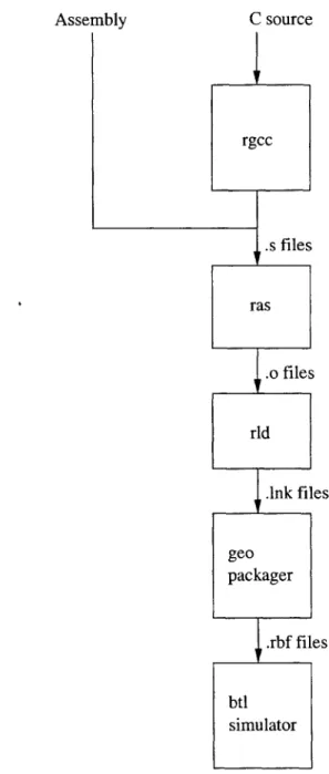
Raw
Overview
The Raw microprocessor is a tiled computer architecture designed in the Computer Architecture Group at MIT. The processor contains 16 replicated tiles in a 4x4 mesh.
A tile consists of a main processor, memory, two dynamic network routers, two static
switch crossbars and a static switch processor. Tiles are connected to each of their four nearest neighbors via register mapped communication by two sets of static network interconnect and two sets of dynamic network interconnect. Each main processor is similar to a MIPS R4000 processor. It is an in-order single issue processor that has 32KB of data cache and 8K instructions of instruction store. The static switch processor handles compile time known communication between tiles. Each static switch processor has 8K instructions of instruction store.
Because of all of the parallel resources available and the closely knit communica-tion resources, many differing computacommunica-tional models can be used to program Raw. For instance instruction level parallelism can be mapped across the parallel compute units as is discussed in [21]. Another parallelizing programming model is a stream model. Streaming exploits course grain parallelism between differing filters which are many times used in signal processing applications. A stream programming lan-guage for the Raw chip is being developed to compile a new programming lanlan-guage named StreamIt [12]. The applications in this study for Raw were written in 'C' and assembly and were hand parallelized with communication happening over the static network for peak performance.
The Raw processor is being built on IBM's SA-27E ASIC process. It is currently out to fab and chips should be back by the end of October 2002. More information can be found in [26].
Tool Flow
Compilation for the Raw microprocessor is more complicated than a standard sin-gle stream microprocessor due to the fact that there can be 32 (16 main processor
rgcc .s files ras .o files rld .lnk files geo packager .rbf files btl simulator
Figure 3-4: Raw Tool Flow
streams, 16 switch instruction streams) independent instruction streams operating at the same time. To solve the complicated problem of building binaries and simulating them on the Raw microprocessor, the Raw group designed the Starsearch build infras-tructure. Starsearch is a group of common Makefiles that the Raw group shares that understands how to build and execute binaries on our various differing simulators. This has saved countless hours for new users to the Raw system by preventing them from having to set up their own tool flow.
Figure 3-4 shows the tool flow used in this thesis for Raw. This tool flow is conveniently orchestrated by Starsearch. The beginning of the tool flow is simply a port of the GNU compilation tool flow of gcc and binutils. geo is a geometry management tool which can take multiple binaries, one for each tile, and create self booting binaries using Raw's intravenous tool. This is the main difference from a standard microprocessor with only one instruction stream. Lastly the rbf file is booted on a cycle accurate model of the Raw processor called btl.
To collect performance statistics for the studied applications on Raw a clock speed of 300MHz. was assumed. Applications were simulated on btl and timed using Raw's built in cycle counters, CYCLEHI and CYCLELO, which provide 64-bits worth of accuracy. Unlike on the Pentium, preheating the cache was not needed. This was because the data that was to be operated and the results all came in and left on the static network. To accomplish this, bC 2 models were written that streamed in and
collected data from the static networks on the Raw chip thus preventing all of the problems that are caused by memory hierarchy.
Area calculations are easily made for the Raw chip because the Raw group has completed layout of the Raw chip. A tile is 4mm. x 4mm. This study assumes that as tiles are added the area scales linearly, which is a good approximation, but is not completely accurate because there is some area around a tile reserved for buffer placement, and there are I/O drivers on the periphery of the chip.
2bC is btl's extension language which is very similar to 'C' and allows for rapid prototyping of
Chapter 4
Applications
4.1
802.11a Convolutional Encoder
4.1.1
Background
As part of the author's belief that benchmarks should be chosen from real applications and not simply synthetic benchmarks, the first characteristic application that will be examined is the convolutional encoder from 802.11a. IEEE 802.11a is the wireless Ethernet standard [17, 18] used in the 5GHz. band. In this band, 802.11a provides for transmission of information up to 54Mbps. Other wireless standards that have similar convolutional encoders to that of 802.11a include IEEE 802.11b [17, 19], the current WiFi standard and most widely used wireless data networking standard, and Bluetooth [3], a popular standard for short distance wireless data transmission.
Before we dive into too much depth of convolutional encoders we need to see where they fit into the overall application. Figure 4-1 shows a block diagram of the transmit path for 802.1Ia. Starting with IP packets, they get encapsulated in Ethernet frames. Then the Ethernet frames get passed into the Media Access Control (MAC) layer of the Ethernet controller. This MAC layer is typically done directly in hardware. The
MAC layer is responsible for determining when the media is free to use and relaying
physical problems up to higher level layers. The MAC layer then passes the data onto the Physical Layer (PHY) which is responsible for actually transmitting the
ISO Layer 802.1 la Blocks Units Passed
V IP Packets
Network Layer IP
Ethernet Frames Data Link Layer MAC
MAC Data Service
Units Physical Layer PHY - PLCP
Encoded Packets PHY - PMD
Modulated Symbols Figure 4-1: 802.11a Block Diagram
data over the media, in this case radio waves. In wireless Ethernet the PHY has two sections. One that handles the data as bits, the physical layer convergence procedure (PLCP), and a second part that handles the data after it has been converted into symbols, the physical medium dependent (PMD) system. 802.11a uses orthogonal frequency division multiplexing (OFDM) which is a modulation technique that is more complicated than something like AM radio.
Figure 4-2 shows an expanded view of the PHY path. The input to this pipeline are MAC service data units (MSDUs), the format at which the MAC communicates with the PHY and the output is a modulated signal broadcast over the antenna. As can be seen in the first box, all data which passes over the airwaves, needs to first pass through forward error correction (FEC). In the 802.11a, this FEC comes in the form of a convolutional encoder. Because all of the data passes through the convolutional encoder, it must be able to operate at line speed to maintain proper throughput over the wireless link. It is advantageous to pass all data that is to be transmitted over a wireless link through a convolutional encoder because it provides some resilience to electro-magnetic interference. Without some form of encoding, this interference
FEC Interleaving and IFFT GI Symbol IQ
Coder Mapping Addition Wave Mod.
Shaping HPA
Figure 4-2: 802.11a PHY Expanded View taken from [18] would cause corruption in the non-encoded data.
There are two main ways to encode data to add redundancy and prevent trans-mission errors, block codes and convolutional codes. A basic block code takes a block of n symbols in the input data and encodes it into a codeword in the output alphabet. For instance the addition of a parity bit to a byte is an example of a simple block code. The code takes 8 bits and maps into 9-bit codewords. The parity operation maps as follows, have all of the first 8 bits stay the same as the input byte and have the last bit be the XOR of all of the other 8 bits. After that one round this block code takes the next 8 bits as input and do the same operation. Convolutional codes in contrast do not operate on a fixed block size, but rather operate a bit at a time and contain memory. The basic structure of a convolutional encoder has k storage elements chained together. The input bits are shifted into these storage elements. The older data which is still stored in the storage elements shift over as the new data is added. The shift amount s can be one (typical) or more than one. The output is computed as a function of the state elements. A new output is computed when-ever new data is shifted in. In convolutional encoders, multiple functions are many times computed simultaneously to add redundancy. Thus multiple output bits can be generated per input bit. Figure 4-3 shows a generalized convolutional encoder. The boxes with numbers in them are storage elements that shift over by s bits every encoding cycle. The function box, denoted with
f,
can actually represent multiple differing functions.As can be seen from the previous description, a convolutional 1 encoder essentially 'Convolutional codes get their name from the fact that they can be modeled as the convolution of polynomials in a finite field, typically the extended Galois field GF(pr). This is typically done by modeling the input stream as the coefficients of a polynomial and the tap locations as the coefficients
-+t~ 1 2 3 4 .. k Bits
utput Bits
Figure 4-3: Generalized Convolutional Encoder
smears input information across the output information. This happens because, as-suming that the storage shifts only one bit at a time (s = 1), one bit effects k output bits. This smearing helps the decoder detect and many times correct one bit errors in the transmitted data. Also, because it is possible to have multiple output bits for each cycle of the encoder, even more redundancy can be added. The rate of input bits compared to the output bits is commonly referred to the rate of the convolutional encoder. More mathematical groundings about convolutional codes can be found in [23], and a good discussion on convolutional codes, block codes and their decoding can be found in [24].
This application study uses the default convolutional encoder that 802.11a uses in poor channel quality. It is a rate 1/2 convolutional encoder and contains seven storage elements. 802.11a has differing encoders for different channel quality with rates of 1/2, 3/4, and 2/3. The shift amount for this convolutional encoder is one
(s = 1). Figure 4-4 is a block level diagram of the studied encoder. This encoder has two outputs with differing tap locations, and uses XOR as the function it computes. The generator polynomials used are go = 1338 and g, = 1718.
of a second polynomial. Then if you convolve the two polynomials modulo a prime polynomial and evaluate the resultant polynomial with x = 1 in the extended Galois field, you get the output bits.
Input
-z-0
_
Figure 4-4: 802.11a Rate 1/2 Convolutional Encoder
4.1.2
Implementations
Verilog
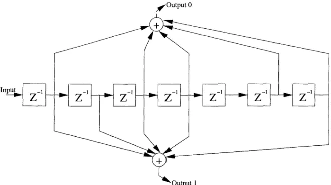
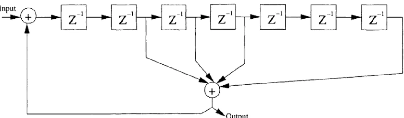
This convolutional encoder and other applications similar to it, which include linear feedback shift registers, certain stream ciphers and other convolutional encoders all share similar form. This form is amazingly well suited for simple implementation into hardware. The basic form of this circuit is as chain of flip-flops serially hooked together. Several outputs of this chain are then logically XORed together producing the outputs of the circuit. For this design, the same code was used for synthesis to both the IBM SA-27E ASIC and Xilinx targets. While this design was not pipelined more than the trivial implementation, if needed, convolutional encoders that lack feedback can be arbitrarily pipelined. They can be pipelined up to the speed of the delay through one flip-flop and one gate but this is probably not efficient due to too much latch overhead.
Encoders with feedback such as those in Figures 4-5 and 4-6, cannot be arbitrarily pipelined. They can be pipelined up to the point where the data is first used to compute the feedback. In this case it is the location of the first tap. Thus for the
Output 0
Inpu Z - - Z - Z - Z - Z 1 - Zlo Z - -~
Output
Figure 4-5: Convolutional Encoders with Feedback
Inpu Z - Z- -w Z- -- oZ-w Z -
---Output
Figure 4-6: Convolutional Encoders with Tight Feedback
encoder shown in Figure 4-5 the circuit can be pipelined two deep, where the first tap occurs. But, the encoder in Figure 4-6 cannot be pipelined any more than the naive implementation provides for.
Not too surprisingly from the fact that these applications were designed to be implemented in hardware, the Verilog implementation of this encoder was the easiest and most straight forward to implement. While the implementation still contains a good number of lines of code, this is not an indication of the difficulty to express this design but rather is due to the inherent code bloat associated with Verilog module declarations.
Pentium
While this application is easily implemented in hardware, when it comes to a software implementation it is less clear what the best implementation is. Thus two implemen-tations were made, one which is a naive 'reference' implementation which calculates
void calc(unsigned int dataIn, unsigned int * shiftRegister,
unsigned int * outputArrayO, unsigned int * outputArrayl)
*outputArrayO = dataIn ^ (((*shiftRegister)>>4) & 1)
(((*shiftRegister)>>3) & 1) ^ (((*shiftRegister)>>1) & 1)
^ ((*shiftRegister) & 1);
*outputArrayl = dataIn ^ (((*shiftRegister)>>5) & 1)
(((*shiftRegister)>>4) & 1) (((*shiftRegister)>>3) & 1)
^ ((*shiftRegister) & 1);
*shiftRegister = (dataIn << 5) I ((*shiftRegister) >> 1);
}
Figure 4-7: Inner-Loop for Pentium reference 802.11a Implementation
the output bits using logical XOR operations and a 'lookup table' implementation which computes a table of 2' entries which contains all of possibilities of data stored in the shift register. Then the contents of the shift register are used as a index into the table. Both of these implementations are written in 'C'. Figure 4-7 shows the inner loop of the reference code.
As can be seen in the reference code, the input bit is passed into the calc function as dataIn, the two output bits are calculated into the locations *outputArrayO and *outputArrayl. And lastly the state variable *shiftRegister is shifted over and the new data bit is added for the next iteration of the loop. This inner loop is rather expensive especially considering how many shifts and XORs need to be carried out in the inner loop.
To make the inner loop significantly smaller, other methods were investigated to put as much as is possible out of the inner loop of this applications. Unfortunately, the operations that needed to be done were not simply synthesizable out of the operations available on a x86 architecture. Hence the fastest way to implement this convolutional encoder was to use a lookup table. The lookup table implementation of this encoder uses the same loop from the reference implementation to populate a lookup table with all of the possible combinations of shift register entries and then in its inner loop, the only work that needs to be done is indexing into the array and shifting of the shift register. Figure 4-8 shows the inner loop for the lookup table version of this encoder. Note that lookupTable [I contains both outputs as a performance optimization and
void calc(unsigned int dataIn, unsigned int * shiftRegister,
unsigned int * outputArrayO, unsigned int * outputArrayl)
unsigned int theValue; unsigned int theLookup;
theValue = (*shiftRegister) I (dataIn<<6); theLookup = lookupTable[theValue];
*shiftRegister = theValue >> 1;
*outputArrayO = theLookup & 1; *outputArrayl = theLookup >> 1;
}
Figure 4-8: Inner-Loop for Pentium lookup table 802.11a Implementation
as such when assigning to the outputs some extra work must be done to demultiplex the outputs.
Raw
On the Raw tiled processor, three different versions of the encoder were made. They were all implemented in Raw assembly. Two of the implementations, lookup table and POPCOUNT, use one tile and the third implementation, distributed, uses the complete Raw chip, 16 tiles. One of the main differences between the Pentium versions of these codes and the Raw versions is the input/output mechanisms. On the Pentium, the codes all encode from memory (cache) to memory (cache), while Raw has a inherently streaming architecture. This allows the inputs to be streamed over the static network to their respective destination tiles and the encoded output can be streamed over the static network off the chip. The inputs and outputs all come from
off chip devices in the Raw simulations.
The lookup table implementation for Raw is very similar to the Pentium version, with the exception that it is written in Raw assembly code, and it uses the static network as input and output. Figure 4-9 shows the inner loop. In the code, register
$8 contains the state of the shift register and $csti is the network input and $csto is
the static network output. The loop has been unrolled twice and software pipelined to hide the memory latency of going to the cache.
loop:
# read the word sl $9, $csti, 6
or $8, $8, $9
# do the lookup here
sll $11, $8, 2 1w $9, lookupTable($11) srl $8, $8, 1 sll $10, $csti, 6 or $8, $8, $10 sll $12, $8, 2 lw $10, lookupTable($12) andi $csto, $9, 1 sri $csto, $9, 1 srl $8, $8, 1 andi $csto, $10, 1 srl $csto, $10, 1
j
loopFigure 4-9: Inner-Loop for Raw lookup table 802.11a Implementation
The Raw architecture has a single cycle POPCOUNT 2 instruction whose assembly mnemonic is popc. The lowest ordered bit of the result of popc is the parity of the input. This is convenient for this application because calculation of the outputs are a mask operation followed by a parity operation. The code of the inner loop of the POPCOUNT implementation can be seen in Figure 4-10. This implementation does not have a significantly different running time than the lookup table version, but it has no memory footprint.
The last and most interesting implementation for the Raw processor is the
dis-tributed version which uses all 16 tiles. This design exploits the inherent parallelism
in the application and the Raw processor. In this design tile computes subsequent outputs. Thus if the tile nearest to the output is computing output x., the tiles further back in the chain are computing newer output values xn+1 to
xn+6-This implementation contains two data paths and output streams which corre-spond to the two output values of the encoder. In this design all of the input data streams past all of the computational tiles. As the data streams by on the static
2
# this is the mask for output bit 0 li $11, (1<<6)1|(1<<4)1|(1<<3)1|(1<<1)1|(1)
# this is the mask for output bit 1
li $12, (1<<6) 1 (1<<5) 1 (1<<4) 1 (1<<3) 1(1) loop:
# read the word
sli $9, $csti, 6 or $8, $8, $9 and $9, $8, $11 and $10, $8, $12 popc $9, $9 popc $10, $10 andi $csto, $9, 1 andi $csto, $10, 1 srl $8, $8, 1
j
loopFigure 4-10: Inner-Loop for Raw POPCOUNT 802.11a Implementation
flu.']
<K >2 >9> >2 ~> <K <K <0IVo III(y 1 1
$
7, tVW\, WN, tvWv ml., Connection Tile Output 0 Computation Output 1 Computation Input Data Flow Output 0 Data Flow Ouput 1 Data Flow4-11: Mapping of the distributed 802.11a convolutional encoder on 16 Raw Figure
network, the respective compute tiles take in only the data that they need. Each tile only needs to take in five pieces of data because there are only five taps in this application, but they need to have all of the data flow past them because of the way that the data flows across the network. Once outputs are computed, they are injected onto the second static network for their trip to the output of the chip. The input and output paths can be seen in Figure 4-11. The connection tiles are needed to bring the output data off-chip because it was not possible to have the output data get onto the first static network without them. Lastly, all of the tiles have the same main processor code which consists of one move, four XORs, and a jump to get to the top of the loop. The static switch code determines which data gets tapped off to be operated on.
While this design might look scalable, it is not linearly scalable by simply making the chains longer. This is because if you make the chains longer, you will find that each tile has to let more data that it doesn't care to see pass by them. The current mapping does as good as a longer chain does because it is properly balanced. Every tile has to have 7 bits of data pass it, but it only cares to look at 5 of those input
values, but because the application is 7 way parallel, it properly matched. If you make the chain longer, the useful work begin done will go from 5/7 to 5/n where n is the length of the chain, and hence no speedup is attained.
4.2
8b/10b Block Encoder
4.2.1
Background
The second characteristic application that this thesis will explore is IBM's 8b/10b block encoder. It is a byte oriented binary transmission code which translates 8 bits at a time into 10-bit codewords. This particular block encoder was designed by Widmer and Franszek and is described in [30] and patented in [9]. This encoding scheme has some nice features such as being DC balanced, detection of single bit errors, clock recovery, addition of control words and commas, and ease of implementation in
hardware.
One may wonder why 8b/10b encoding is important. It is important because it is a widely used line encoder for both fiber-optic and wired applications. Most notably it is used to encode data right before it is transmitted in fiber optic Gigabit Ethernet [20] and 10 Gigabit Ethernet physical layers. Also, because it is used in such high speed applications, it is a performance critical application.
This 8b/10b encoder is a partitioned code, meaning it is made up of two smaller encoders, a 5b/6b and a 3b/4b encoder. This partitioning can be seen in Figure 4-12. To achieve the DC balanced nature of this code, the Disparity control box contains one bit of state which is the running disparity of the code. It is this state which lets the code change its output codewords such that the overall parity of the line is never more than ±3 bits, and the parity at sub-word boundaries is always either +1 or
-1. The coder changes its output codewords by simply complementing the individual subwords in accordance with the COMPL6 and COMPL4 signals. All of the blocks in Figure 4-12 with the exception of the Disparity control simply contain feed forward combinational logic therefore this design is somewhat pipelinable. But due to the tight parity feedback calculation it is not inherently parallelizable otherwise. Tables are provided in [30] which show the functions implemented in these blocks, along with a more minimal combinational implementation.
4.2.2
Implementations
Verilog
Two implementations were made of this 8b/10b encoder in Verilog and they were shared between the IBM ASIC process and the Xilinx FPGA flows. One which we will call non-pipelined is a simplistic reference implementation following the proposed implementation in the paper. One thing to note about this implementation is that in the paper, two state elements were, and two-phased clocks were used while both of these were not needed. A good portion of the time designing this circuit was spent figuring out how to retime the circuit not to use multi-phase clocks. Unfortunately
Input Data 8 10 Output Data 6b control 5 5b 5 5b/6b functions encoding Disparity control
(State inside) COMPL4
3 3b 33b/4b
374 3bcton 37 encoding
- fuctios & switch
Control/ II3b control _
Data
Figure 4-12: Overview of the 8b/10b encoder taken from [30]
due to the retiming, a longer combinational path was introduced in the Disparity control box. This path exists because the parity calculation for the 3b/4b encoder is dependent on the parity calculation for the 5b/6b encoder.
To solve the timing problems of the non-pipelined design, a pipelined design was created. Figure 4-13 shows the locations of the added registers to the design. This design was conveniently able to reuse the Verilog code by simply adding the shown registers. The pipelined design was pipelined three deep. This is not the maximal pipelining depth, but rather this design can be pipelined significantly more, up to the point of the feedback in the parity calculation which cannot be pipelined.
Pentium
This application has only one feasible implementation on a Pentium. This implemen-tation is as a lookup table. This was written in 'C' and the lookup table was created
by hand from the tables presented in [30]. To increase performance, one large table
was made thus providing a direct mapping from 9 bits (8 of data and one bit to denote control words) to 10 bits. The inner loop of the lookup table implementation can be
8 + 5b functions ... 3b functions
-LIP
6b control 3b control Input Data 5 COMPL 6 COMPL4 :3 1:2 4-10 Output DataFigure 4-13: 8b/10b encoder pipelined
unsigned int bigTableCalc(unsigned int theWord, unsigned int k)
unsigned int result;
result = bigTable[(disparityO<<9)I(k<<8)I(theWord)]; disparityO = result >> 16;
return (result&Ox3ff);
}
Figure 4-14: Inner-Loop for Pentium lookup table 8b/10b Implementation seen in Figure 4-14. The code constructs the index from the running disparity and the input word, does the lookup, and then saves away the running disparity for the next iteration.
Raw
On Raw, a lookup table implementation was made and benchmarked. This design was written in 'C' for the non-critical table setup, and Raw assembly for the critical portions. It is believed that a 'C' inner-loop implementation on Raw could do just as good, but currently it is easier to write performance critical Raw code that uses the
5b/6b encoding switch 5 :3 Control/ Data Disparity control (State inside) 0: 1 3b/4b encoding switch
loop:
# read the word
or $9, $csti, $8 # make our index
sll $10, $9, 2 # get the word address
lw $9, bigTable($10) # get the number
or $0, $0, $0 # stall or $0, $0, $0 # stall
andi $csto, $9, Ox3ff # send lower ten bits out to net
srl $8, $9, 7 andi $8, $8, Ox200
j loop
Figure 4-15: Inner-Loop for Raw lookup table 8b/10b Implementation
networks in assembly. Figure 4-15 shows the inner-loop of the lookup table. bigTable contains the lookup table. The two instructions marked with stall are there because there is an inherent load-use penalty on the Raw processor. Unfortunately due to the tight feedback via the parity bit, software pipelining is not able to remove these stalls. Some thought was given to trying to make a pipelined design for Raw much in the same way that this application was pipelined in Verilog. Unfortunately, the speed at which the application would run would not change because the pipeline stage which contains the disparity control would have to do a read of the disparity, a table lookup, and save off of the the disparity variable which has an equivalent critical path to the
lookup table design. It would save table space though by making the 512 entry table
into three smaller tables, but this win is largely offset by the fact that it would require more tiles and the 512 word table already fits inside of the cache of one tile.
Chapter 5
Results and Analysis
5.1
Results
As discussed in Chapter 3, generating a fair comparison between so largely varied architectures is quite difficult. This thesis hopes to make a fair comparison with the tools available to the author. The area and frequency numbers in this section are normalized to a 0.15pm. Ldrawn process. This was done by simply quadratically 1
scaling the area and linearly scaling the frequency used. No attempt was made to scale performance between technologies to account for voltage differences. This linear scaling is believed to be a relatively good approximation considering that all of the processes are all very similar 0.18pm. vs. 0.15pm. vs. 0.13pm.
5.1.1
802.11a Convolutional Encoder
Table 5.1 shows the results of the convolutional encoder running on the differing targets. The area and performance columns are both measured metrics while the performance per area column is a derived metric. Figure 5-1 shows the absolute, normalized to 0.15pm., performance. This metric is tagged with the units of MHz. which is the rate at which this application produces one bit of output. The trailing letters on the Pentium identifiers denote which cache the encoding matrices fit in. 'This should be quadratically scaled because changing the feature size scales the area in both directions thus introducing a quadratic scaling term.
Target Implementation Area (mm2) Performance
Performance (Normalized to (MHz.) per Area
0. 15pm. Ldrawn) (Normalized) (MHz./mm 2
.)
IBM SA-27E 0.0016670976 1250 749806
ASIC
Xilinx Virtex II 0.77 364 472.7
Intel Pentium 4 reference Li 194.37 50.1713 0.2581
Northwood reference L2 194.37 48.9 0.2515
2.2GHz. reference NC 194.37 46.5 0.2393
Normalized to lookup table Li 194.37 119.2 0.6131
1.907GHz. lookup table L2 194.37 95.3 0.4905
lookup table NC 194.37 76.3 0.3924 Intel Pentium 3 reference Li 73.61 27.1 0.3678
Coppermine reference L2 73.61 24.312 0.3303
993MHz. reference NC 73.61 18.6 0.2530
Normalized to lookup table Li 73.61 74.5 0.1.0117
1191.6MHz. lookup table L2 73.61 62.7 0.8519
lookup table NC 73.61 25.2 0.3423
Raw 1 tile lookup table 16 31.57 1.973
300 MHz. POPCOUNT 16 30 1.875
Raw 16 tiles distributed 256 300 1.172
300 MHz.
Table 5.1: 802.11a Convolutional Encoder Results
"Li" represents that all of data fits in the Li cache, "L2" the L2 cache, and "NC" represents no cache, or the data set size is larger than the cache size.
Figure 5-1 shows trends that one would expect. The ASIC implementation pro-vides the highest performance at 1.25GHz. The FPGA is the second fastest at ap-proximately 4 times slower. Of the microprocessors, the Pentium 4 shows the fastest non-parallel implementation. The Raw processor provides interesting results. It is significantly slower than the Pentium 4 using a single tile, which is to be expected considering that the Raw processor runs at 300MHz. versus 2GHz. and is only a single issue in-order processor. But by using Raw's parallel architecture a parallel mapping can be made which provides 10x the performance of one tile when using all
16 tiles. Note that this shows sub-linear scaling of this application. These
perfor-mance numbers show for a real world application how much more adept an ASIC is than an FPGA and how much more adept a FPGA is than a processor at bit level