HAL Id: tel-02181856
https://tel.archives-ouvertes.fr/tel-02181856
Submitted on 12 Jul 2019HAL is a multi-disciplinary open access archive for the deposit and dissemination of sci-entific research documents, whether they are pub-lished or not. The documents may come from teaching and research institutions in France or abroad, or from public or private research centers.
L’archive ouverte pluridisciplinaire HAL, est destinée au dépôt et à la diffusion de documents scientifiques de niveau recherche, publiés ou non, émanant des établissements d’enseignement et de recherche français ou étrangers, des laboratoires publics ou privés.
Synthesis of ferroelectric oxides for photovoltaic
applications
Alessandro Quattropani
To cite this version:
Alessandro Quattropani. Synthesis of ferroelectric oxides for photovoltaic applications. Condensed Matter [cond-mat]. Université de Strasbourg, 2018. English. �NNT : 2018STRAD053�. �tel-02181856�
UNIVERSITÉ DE STRASBOURG
ÉCOLE DOCTORALE Mathématiques, Science de l’Information et de l’Ingénieur
UMR 7357
THÈSE
présentée par :Alessandro QUATTROPANI
soutenue le : 17 Décembre 2018
pour obtenir le grade de : Docteur de l’université de Strasbourg Discipline/ Spécialité
: Science des Matériaux
Synthesis of Ferroelectric Oxides for
Photovoltaic Applications
THÈSE dirigée par :
M.SLAOUI Abdelilah Directeur de recherche, ICube, CNRS-Université de Strasbourg
RAPPORTEURS :
M.EL MARSSI Mimoun Professeur, LPMC Université de Picardie Jules Verne, Amiens
Mme. BESLAND Marie-Paule Directrice de recherche, Institut des Matériaux Jean Rouxel, Nantes
AUTRES MEMBRES DU JURY :
Mme. VIART Nathalie Professeur, IPCMS, CNRS-Université de Strasbourg
MEMBRES INVITÉ :
M. DINIA Aziz : Professeur, IPCMS, CNRS-Université de Strasbourg
M. FIX Thomas Chargé de recherche, ICube, CNRS-Université de Strasbourg M. REHSPRINGER Jean-Luc Directeur de recherche, IPCMS, CNRS-Université de Strasbourg
2
3
Aknowledgements
First I would like to thank my Thesis Director, Dr. Abdelilah Slaoui, for continual guidance and assistance throughout the duration of my Ph.D., and without whom this work would not have been possible. Even, its high support allowed my personal career growth by putting at disposal his work knowledge.
I would like to thanks the members of jury Mimoun El Marrsi, Marie-Paule Besland, Nathalie Viart, Aziz Dinia, Thomas Fix, Jean-Luc Rehspringer, not only for have made through Strasbourg even if the chaos of the recent events but even for their interest in my work and suggestions and corrections to this manuscript which increase the value of this work.
I should give particular thanks to the contributions to this work to my supervisor Dr.Thomas Fix. He made vital contributions to most of the work and gave me invaluable help on a totally new research topic for me. His patience and wise allowed me to growth familiar with the research environment and pushed me to the end of these three years.
Another special thanks should be given to Prof. jean-Luc Rehspringer , for his invaluable help on chemical processes and for having putting his experience on the work in order to make big steps in the work. I should thank Professor Aziz Dinia, which allowed me to work independently in IPCMS, which collaboration allowed a huge breakthrough in the work.
Another special thank should go to Dr.Guy Schmerber, for his patience and understanding during my PhD project as well as willing to accomplish the work in very limited time laps. My PhD would have not be the same without his support.
A huge thanks to Cristophe Lefevre, which allowed me to work with him at the Synchrotron which allows a big step forward in this research project.
A big thanks will go to Damien Aureau and Mathieu Fregnaux for the XPS measurements that will put this work of 3 years under a new light; I would like to thank even Judith Driscoll which allowed a collaboration with the University of Cambridge where I have learnt more about the Kelvin Probe Force Microscopy. A special thanks to the people who helped me during this work; in this sense I would like to thank Silviu Colis, Gilles Versini, Mircea Rastei, Bohdan Kundys, Daniel Stoeffler, Cristophe Lefevre, Cedric Leuvrey, Gérald Ferblantier, Dominique Muller, Sophie Barre and all the people who helped me during these 3 years.
A particular thought to Stephan Roques and Florian Mugler, which not only were always avaible for help but even with their sympathy made my life in the laboratory more easy and less stressing.
Eventually I would like to say a special thanks to the PhD and Post-Docs and Master’s students who were with me in the laboratory especially I would like to thank Anatolie Graviluta, which is huge support and joyness during these 3 years.
I should eventually mention all my Italian friends I met in Strasbourg which made my life way more easy and funny. I have found special people which I will be in contact for long and tat will always will make me feel a little bit more home wherever I will go.
1
Table of contents
Chapter 1. ... 3
Photovoltaics: an overview ... 3
1.1. Photovoltaics: principle ... 4
1.1.1. The solar spectrum ... 4
1.1.2. The absorption of the sun light... 5
1.1.2. The absorbing material ... 6
1.1.3. Photovoltaic Effect ... 6
1.1.4. Efficiency limiting factors... 9
1.1.5. The Shockley-Queisser Limit ... 10
1.2. Materials for Photovoltaic ... 12
1.2.1. Solar cells Technologies: state of the art ... 12
1.2. Oxides materials for Photovoltaics ... 17
1.3.Summary ... 20
References of Chapter 1: ... 21
Chapter 2. ... 24
Perovskite oxide based devices ... 24
2.1. Structure of perovskite oxides ... 25
2.2. Typical properties of perovskite oxides ... 28
2.3. The double perovskite ... 29
2.3.1 Ordering in double perovskite ... 30
2.4. Multiferroic perovskite oxide for Photovoltaics ... 33
2.4.1. Ferroelectricity ... 33
2.4.2. Ferromagnetism ... 34
2.4.4. Multiferroicity ... 35
2.4.5. The case of Bi2FeCrO6 ... 36
2.4.6. Tuning the Bandgap ... 40
2.5. Photovoltaic Effect in Ferroelectric Perovskite ... 40
2.5.1. Bulk Photovoltaic Effect ... 41
2.5.2. Domain Walls ... 44
2.5.3. Ferroelectric Photovoltaic Evaluation ... 46
2.5.4. Working Mechanism of Ferroelectric Solar Cell... 47
2.5.5. The role of the electrodes ... 49
2.5.6. Current Switching ... 51
2
2.6. Summary ... 53
References of Chapter 2 ... 54
Chapter 3. ... 59
Properties of BFCO deposited by sol-gel technique ... 59
3.1. Sol-gel solutions preparation:... 59
3.2. Powder preparation and Thermo-Gravimetrical Analysis-Differential Thermal Analysis ... 60
3.3. BFCO layer deposition ... 64
3.3.1. CTA of sol-gel BFCO solutions ... 64
3.3.2.Structural properties of the films ... 65
3.3.3. RTA of sol gel BFCO films ... 73
3.4. Conclusions ... 77
References of chapter 3 ... 78
Chapter 4. ... 79
Properties of BFCO grown by the Pulsed Laser Deposition Technique... 79
4.1 Experimental procedure ... 79
4.2. Effects of the deposition conditions on structural properties ... 80
4.2.1. Deposition Temperature ... 80
4.2.2. Oxygen partial pressure ... 81
4.2.3. Laser Energy ... 82
4.2.4. Laser repetition rate ... 83
4.2.5. Thickness effect ... 89
4.3. AB Initio Calculations for the Order effect ... 92
4.4. Electrical properties of the PLD BFCO films ... 98
4.4.1. Samples preparation... 98
4.4.2 . KPFM on ITO/BFCO/Nb:STO ... 99
4.4.3. Ferroelectric properties of the PLD-BFCO films ... 101
4.4.4. PFM Measurements on PLD-BFCO samples ... 102
4.4.5. Photoelectric effect on BFCO films ... 104
4.4.6. Photovoltaic effect of PLD-BFCO samples ... 110
4.5. Conclusions ... 120
References of chapter 4: ... 121
Conclusions and perspectives ... 123
3
Chapter 1.
Photovoltaics: an overview
During the last decade, humankind have undergone a strong energetic challenge since the technological advance and the high rate of development of emergent countries, such as China, India and Brazil, have followed a huge energy request. Consequently, a high energy demand at low cost are requested to satisfy the global needs. On the other hand, the scarcity of fossil fuels and the recent global weather changes pushed scientist to look forward to implement solutions of green energy production. Among the renewable energy options, photovoltaic energy, consisting in converting the sun radiation to electricity, has been intensively studied because of the large amount of energy received every day by our planet from the sun. In fact, in only one hour the sun irradiates the earth with a quantity of energy which would satisfy the global needs per years. The photovoltaic technologies advanced a lot since the discovery by Einstein1 of the photoelectric effect and the first solar cells developed at Bell’s laboratory in 1950. For many years the commercialized silicon panel were too expensive to compete with fossil fuels2, thus the photovoltaic energy remains for years only exclusive for special applications such as energy generation for satellites or off-grid connected zones. In more recent years, thanks to research and advances in PV technologies and a large development of equipment and automation, a huge drop in costs occurred which make photovoltaics enough competitive with conventional energy production methods. This drop stimulated the research and development of the PV technology; it can be pointed out that in 2017, 98.9 GW of solar panels have been installed worldwide as compared to less than 20 GW in 2010. Fig.1.1 summarizes this large increment by plotting the installed solar capacity between 6 big groups worldwide. It is noticeable how the huge development nowadays is linked especially to the emergent markets in China, and more generally, in the Asian-Pacific countries (APAC).
4
Fig.1.1.Worldwide solar panel energy installation from 2000 to 2017 3
1.1. Photovoltaics: principle
1.1.1. The solar spectrum
In order to introduce the solar cell devices, it is important to get familiar with the photovoltaic technology. The energy is provided by the sun, which behaves as a black body at 5800 K and its emission band is optimal at a wavelength of 500 nm. The average solar irradiation outside of the atmosphere has a power of 1366 W/m2. When the solar radiation enters the atmosphere, it gets weighted by different factors: the different layers of the atmosphere, weather conditions well as the longitude and observation height. The gases which are composing the atmosphere (as Ozone (O3), carbon dioxide (CO2) and water vapour) absorbs the radiations close to their binding energy, so that the visible spectra presents some “features” as shown in fig.1.2. Solar irradiation varies at different position on earth so that a reference called “Air Mass” (AM) has been established in order to compare the different irradiation in different part of the globe. Two standards are defined for terrestrial use. The standard spectrum for space applications is referred to as AM0. It has an integrated power of 1366.1 W/m2. The AM1.5 Global spectrum is designed for flat plate modules and has an integrated power of 1000 W/m2 (100 mW/cm2). The AM1.5 Direct (+circumsolar) spectrum is defined for solar concentrator work. It includes the direct beam from the sun plus the circumsolar component in a disk 2.5 degrees around the sun. The direct plus circumsolar spectrum has an integrated power density of 900 W/m2.
5
Fig.1.2. Solar Spectrum at different irradiation energy. Modified from4
1.1.2. The absorption of the sun light
Semiconductors present an energy gap between the valence and the conduction bands which varies typically between 0.3 to 3 eV. When a photon with an energy higher than the bandgap reaches the semiconductor it can be absorbed by the material and an electron can be promoted to the conduction band, leaving in the valence band a pseudo-charge of opposite sign, the hole.
6 In fig.1.3 are presented two types of possible transition which depends on the nature of the bandgap. When the valence band maximum and conduction band minimum are coincident in the K-space, the material has a direct bandgap (fig.1.3.a); the transition is vertical and it is radiative: This is the case, for example, for GaAs, which find different applications in optoelectronics as well as solar cell for space applications. In the case of Silicon, instead, the bandgap is indirect: in this case the valence band maximum and conduction band minimum are not coincident in the K space and the electronic transition are not vertical, so non-radiative because they imply a change in the wave vector of the electron. In this case, in order for a photon to be absorbed, either it has sufficient energy to get promoted to a relative minimum (and then will relax in the absolute minimum by thermalization) or the transition will occur with the help of a phonon absorbed (or emitted) by the electron (fig.1.3.b).
1.1.2. The absorbing material
The solar cell device is based on an absorbing material which should be able to absorb the incident photons, create the hole-electron pairs as well as to separate them in order to collect them and consequently generate a current. Only few materials are able to strike as a solar cell absorber. The most important parameters for a solar cell needs are
• Concentrations of doping atoms; this can be of two types; donor atoms which donate free electrons, ND, or acceptor atoms, which accept electrons, NA. The concentrations determine the width of a space-charge region of a junction.
• Mobility µ, and diffusion coefficient, D, of charge carriers that characterize carriers transport due to drift and diffusion, respectively.
• Lifetime τ, and diffusion length, L, of the excess carriers that characterize the recombination-generation processes
• Bandgap energy, EG, absorption coefficient, α, and refractive index, n, which characterize the ability of a semiconductor to absorb visible and other radiation
1.1.3. Photovoltaic Effect
Electron-hole separation is generally possible in solar cell devices thanks to a potential barrier present within the semi-conductor. The most common type of barrier are the homojunction (which is a p-n junction of the same semiconductor); heterojunction (p-n junction of two different materials) and Schottky barrier (metal/semiconductor). In the case of a silicon solar cell, the most used solution is a homojunction doped p and n, as shown in fig.1.4:
7
Fig.1.4. Band diagram of a p-n junction solar cell5
The generated photocarriers upon absorption and separation have a different behaviour that depends on the zone where they have been created:
• In the p or n zone, the minority carriers which reach the depletion zone are drifted from the electric field to the p-zone (the holes) and to the n-zone (the electrons) where they become majority carriers. A diffusion photo-current will be set into the system • In the depletion zone, the electron-hole pair created by incident photons are
dissociated by the electric field; the electrons move to the n zone and the holes to the p zone. In this case a generated photo-current is set.
These two currents give the total photocurrent Iph which is proportional to the light intensity and it opposes to the diode current Iobs which comes from the polarization of the material. The resulting current will be:
I (V) = Iph-Iobs (V) (eq.1.1) For a ideal solar cell, equation 1.1 takes this form: I (V) = Iph- Is (exp (qV/kT) -1) (eq.1.2)
where Is is the saturation current of the diode; q the elemental charge; k the Boltzmann’s constant and T the Temperature.
8 Under light, the solar cell characteristic of an ideal solar cell is the addition of a current of intensity Iph and the characteristic of this diode in darkness. As a convention, the I/V curve is represented as the inversion of the current axis, so a typical Photovoltaic curve for a p-n junction based device looks like the curve in Figure 1.5:
Fig.1.5. Conventional representation of a photovoltaic I-V curve for a p-n junction based
device6 The important factors in the I-V curve are:
• Isc: the short-circuit current (obtained for V=0)is the current due to the generation and collection of light-generated carriers. For an ideal solar cell at most moderate resistive loss mechanisms, the short-circuit current and the light-generated current are identical. Therefore, the short-circuit current is the largest current which may be drawn from the solar cell.
• Voc: the open-circuit current (obtained for I=0)is the maximum voltage available from a solar cell. The open-circuit voltage corresponds to the amount of forward bias on the solar cell due to the bias junction with the light-generated current.
• Im: the current obtained at the maximum power of the solar cell; • Vm: the voltage obtained at the maximum power of the solar cell.
9 • The Fill Factor (FF): is the parameter which allows the determination of the efficiency of the solar cell together with the Voc and Isc. Graphically, the FF is a measure of the "squareness" of the solar cell and is also the area of the largest rectangle which will fit in the IV curve. The FF is the square represented in fig. 1.X and can be calculated as : FF= (VmIm)/(VocIsc) (eq.1.3)
• The solar cell efficiency (η) which can be expressed as: η= (maximum electrical power)/ (incident Solar power): η= (VmIm)/φi = (FF VocIsc)/ φs (eq.1.4)
where φi it’s the light flux received by the solar cell for a given surface; These parameters vary with the light intensity, so the convention is to use standard conditions at AM 1.5 at a T=25 °C.
1.1.4. Efficiency limiting factors
The photons conversion is not perfect, there are several factors which limits the efficiency of the solar cell. These losses can be classified in two types: 1) losses due to the material; 2) losses due to the technology used.
a) Losses attributed to the material properties:
The main losses in a silicon based solar cell as an example are shown in fig.1.6. The green part is that of the solar spectra effectively used by Silicon for electron-hole conversion. Photons with a wavelength higher than the one of the bandgap (λ>λg) do not have enough energy to promote an electron from the valence band to the conduction band and it is therefore lost (red part of the spectra in fig.1.6). On the other hand, the photons with an energy higher than the one of the bandgap (purple and blue in the spectra) give rise to only one electron-hole pair and the rest of the energy is lost as heat (thermalization).
10
Fig.1.6. Solar Spectrum and loss into a Si based solar cell device4
Other losses are due to a non-perfect Fill Factor. As seen above, the I-V curve depends on the Boltzmann equation under an exponential form (exp (qV/kT) -1); the curve has not a rectangular shape and it is not higher than 0.89 in the best cases. These effect are due to a not perfect p-n junction, the resistance.
b) Losses attributed to the device fabrication:
One important loss in a silicon solar cell is the optical reflection. In fact, the refractive index of Silicon is different from the ones of the air so that at the interface air/Silicon some reflection would low the number of photons which reaches the absorbing material; another optical loss is the shadow effect due to metallic contacts that reflect the impinging sun light.
Finally, the absorption efficiency is important, especially for thin films (<100 µm) because a fraction of the photons which have enough energy get across the cell without being absorbed; the efficiency of collection is instead linked to the number of carriers generated and the ones which are finally collected. These are related to the number of carriers which recombines before being collected and depends on the lifetime of minority carriers (average time between the generation and recombination of a minority carrier).
1.1.5. The Shockley-Queisser Limit
The simple solar cell is based on the PN junction concept. Shockley and Queisser7 were the first to develop a model which took into consideration a single-junction solar cell, in order to
11 establish the maximum theoretical efficiency of an ideal device. To do so, they started from some hypothesis:
• The sun behaves like a black body at a T=6000K; • The solar cell behaves like a black body at T=300 K;
• The solar cell absorbs all the photons with an energy higher than its bandgap;
• Each absorbed photon generates an electron-hole pair which gets immediately dissociated at a rate of 100%;
• The recombination is only radiative;
• Each not recombined charge carrier is efficiently collected.
Using this model, the number of electrons generated in a solar cell is equal to the number of photons with an energy higher than the bandgap of the material minus the number of photons emitted by radiative recombination. In this way it is possible to calculate the maximum efficiency of a solar cell, which is 33.7% for a bandgap of 1.34 eV while it is 31% for the Silicon with a bandgap of 1,12eV, In fig.1.7 are shown (a) the curve calculated by Shockley and Queisser in their article (considering the sun as a black body at 6000 K) and (b) the one modified for a realistic solar spectrum.
1.7. a) curve calculated by Shockley and Queisser in their article7 (considering the sun a 6000 K) and (b) curve modified for a realistic solar spectrum8.
12
1.2. Materials for Photovoltaic
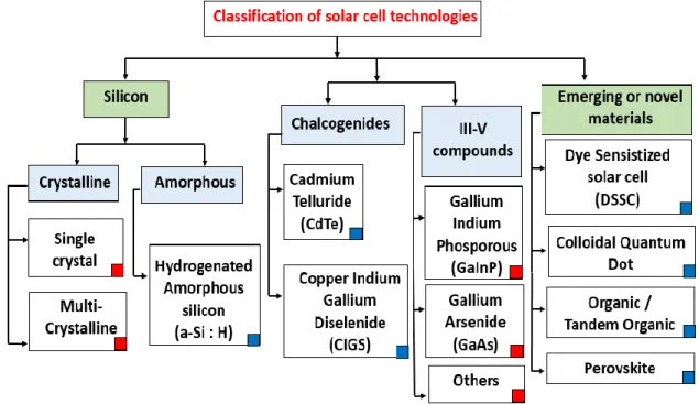
Fig. 1.8 gives a generic view of the present photovoltaic device technologies based on the primary active materials. The established technologies are wafer-based solar cells (crystalline silicon and III-V compounds) or thin films (a-Silicon and Chalcogenides). Also represented are the emerging solar cells technologies such as those based on organic (polymers, small molecules), on hybrid materials (DSSC, perovskite) or using nanomaterials (dots, wires…).
Fig.1.8. Solar cells classification based on the active material. Modified from9
1.2.1. Solar cells Technologies: state of the art
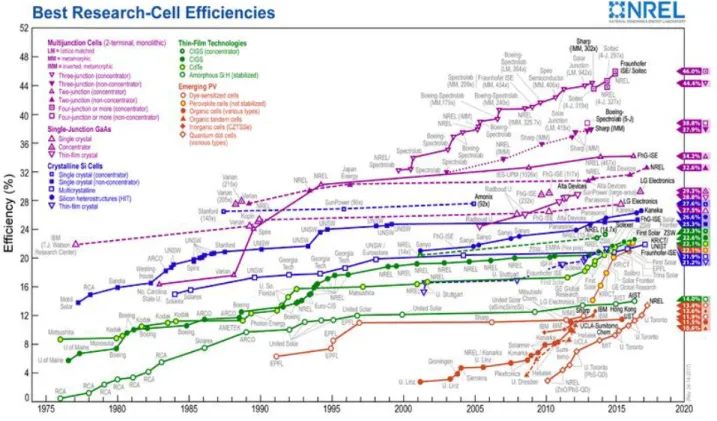
Figure 1.9 shows the graph established by the National Renewable Energy Laboratory (NREL) that summarizes the highest efficiencies reported since 1975. Several technologies and materials are employed to make solar cells. Let’s consider first the single junction (one semiconductor) solar cells structures.
13
Fig.1.9.Highest efficiencies devices reported from 1975 till now10
Figure 1.10.a shows a schematic of a conventional solar cell structure based on single-crystalline or multisingle-crystalline silicon wafers, 150 to 250 m thick. The structure exhibits a conventional P-N homojunction where P region is a boron-doped silicon substrate and the N region is a phosphorous-doped silicon emitter. The backside contact is a screen printed Aluminium layer while the front contact is silver based screen printed through a mask. This structure is the most used to make modules and represents about 90% of the market share. Fig. 1.10.b displays the schematic of an amorphous silicon based solar cell. In this case, the absorbing layer is an intrinsic amorphous silicon layer of about 1-2 m thick, sandwiched between very thin (few nanometres) n and a p doped regions. The front contact is a transparent conducting oxide or TCO (in this case SnO2) and the back contact is an Al film. The whole structure is deposited on a glass serving as a substrate and as a window for solar radiation.
Fig.1.10.c it is a schematic of a solar cell based on Cadmium Telluride (CdTe) which has experimented a huge increase of the market share and have surpassed a-Si technologies in thin films photovoltaic market thanks to their high quantum efficiencies. This structure uses a heterojunction with a n-type semiconductor which is CdS and a p-type one which is CdTe.
14 Similar structures to CdTe Cell but not represented here is that using inorganic compound CIGS (copper-Indium-Gallium-diSelenide) as the absorbing material which has achieved solar efficiencies well above 20%11. The challenge to create solar cells materials with earth-abundant and non-toxic elements pushed to the development of copper-zinc-tin-sulphide (CZTS) thin film compounds. CZTS is a quaternary compound with a direct bandgap of 1.5 eV and a large absorption12 . Yet, the highest efficiency of these CZTS cells was found to be 12.6% in laboratory13. The main drawback of the CIGS and CZTS cells is the synthesis of the layers with the appropriate stoichiometry and free of secondary phases which often leads to inhomogeneous films and recombination centres
Fig.1.10. Schematic of (a) a conventional silicon solar cell; (b) an amorphous silicon solar
cell, (c) a CdS-CdTe solar cell9
Among other cell structures, GaAs based solar cells are established since a decade. This III-V material is well suited for photovoltaic applications as the electrons move faster within this semiconductor as compared to Silicon; moreover, it forms a single junction III-V semiconductor which is well suited in terms of absorption, non-radiative energy loss, minority carrier lifetime and mobility. However, the high fabrication cost of these cells did not allow a large implementation in the market despite an efficiency of 28.8% as a cell and 24.1% in modules. Table 1.1 highlights the established PV technologies and the corresponding maximum efficiencies for the upper mentioned structures.
15
Solar cell Maximum PCE References
c-Si 26.6% Yoshikawa et al.14
a-Si 13.4% (multijunction) LG solar
CdTe 21%(lab)/17.5%(module) First Solar
CIGS 20.3% Jackson et.al.15
GaAs 28.8%(lab)/24.4%(module) Matsubara et al.16
CZTSSe 12.6% Wang et al. 13
Table 1.1. Established technology solar cells and their maximum reported efficiencies
Figure 1.9 shows also that new type of solar cells has emerged more recently. Among them, organic photovoltaics using semiconductor polymers or small molecules as absorbing materials. The main advantages are low temperature deposition, the use of coating methods, printable on several substrates as well as low weight Finally, the tandem organic solar cells were investigated to increase the 11% record efficiency of the single-junction one, and thus it was possible by using an interconnection layer to reach 12.5% efficiency in 201617. Another important advantage of these solar cells is that the dye have a very high absorption coefficient18,19 which can allow even to few nanometres to absorb enough light to reach a high efficiency, although they shows a low dielectric constant. Several works have addressed Bulk Heterojunction Solar cells (BHJ) and DSSC20–25 structures and an efficiency of 12.9% has been achieved with DSSC26 and 8% for BHJ27. Liquid junction QDSC using quantum dots has instead improved till 5% while a 7% efficiency has been reported for a solid state one 22,23 until development of a very recent colloidal quantum dots which showed a 13.4% efficiency28. One important problem of these cells is related to the stability of the absorber material, which should be overcome to widespread these cells in the market.
Recently, a new class of material which involves organic and inorganic Perovskites got renewed interest among researchers. As it will be further discussed in the next chapter, Perovskites are compounds with formula ABX3, where A and B are two cations (normally A has a larger ionic radii than B) and X is an anion, and they have shown an unprecedented increase in efficiency from 3% reported in 2009 29 to more than 22% this year10,30,31, which is
16 comparable with the ones of CdTe and CIGS. What really strikes out in these cells is the large diffusion length and high mobility paired with a low recombination rate at surface and at the grain boundaries. Fig.1.11. displays a schematic of a typical organic-inorganic perovskite cell device.
Fig.1.11. Schematic representation of an Organic-Inorganic perovskite solar cell
The results obtained for these devices are promising. However, several questions have to be answered before such cells penetrate the PV market. Firstly, the toxicity and environmentally dangerous lead can be detrimental for a wide use of the devices. Many researchers respond to this issue saying that the presence of lead is pretty small compared to other commonly used devices (i.e. cars batteries) and therefore this should not be a limiting factor. Secondly, the stability of the hybrid perovskites (as well as the organic compounds for Organic solar cells) is still a questionable point. Recent studies have pointed out the possible large stability of the material. Finally, the manufacturing steps of these cells are still mainly at the laboratory level, and it is far from an industrial pathway when compared to the other technologies.
The table 1.2. summarises the devices based on alternative PV technologies and their maximum reported efficiencies.
As reported in figure 1.8 (NREL chart above), multijunctions solar cells based on III-V materials for ultra-high efficiencies were also developed since many years. In theory, such devices formed by stacking 2 or more III-V semiconductors of different bandgaps can reach an optimal efficiency of about 60% under sun concentration. In practice, multjunctions solar cells with an efficiency approaching 46% has been reported from Fraunhofer Institute for Solar Energy Systems ISE, Germany However, the cell cost increases with increasing the number of
17 junctions so they have found applications mainly in space power generation or under sun radiation concentration higher than 1000.
Solar cell Maximum PCE References
DSSC 12.6% Ren et al.32
Perovskite 22.1% Yang et al.33
Organic 11.2% Mori et al.34
Organic Tandem 12.50% Li et al.17
Quantum Dots 13.4% Sanehira et al.28
Table 1.2. Alternative solar cells technologies and their maximum reported efficiencies
Based on this short review of PV technologies and on data of figure 1.8 (NREL), It can be pointed out that there were continuous investigations over years either (i) by continuously improving the existing technologies by reducing the losses (optical and electrical) or by developing new cell architectures (PERC, PERT, Bifacial, HTJ…), or (ii) by proposing new absorbing semiconductors (organics, hybrids, QDs…) but still using the “junction” concept for charge carriers’ separation.
This thesis’ work is aiming at pursuing option (ii) and proposing inorganic perovskite oxides (POs) as absorbing material but with a completely different concept for charges separation and transport, thanks to the ferroelectric character of these POs.
1.2. Oxides materials for Photovoltaics
Oxide materials offers a wide range of different possible applications in electronics, memory, magnetoelectronics and even bioprocessing35–38. More recently, Oxides for photovoltaic is arising interest for their peculiar characteristics. In particular, Metal Oxides (MO) seems adequate to offer an alternative to the present photovoltaic structures, thanks to their chemical stability and non-toxicity and also easy fabrication. The most known MOs for photovoltaics are the transparent conducting oxides (TCO) which are already widely used in
18 several solar cell structures as front or bottom electrodes thanks to their specific properties (bandgap, work function, carrier mobility and resistivity) which allows an appropriate choice to build a device. The most common MOs are ITO, FTO, ZnO, AZO, SnOx35. For example, in CdTe- based solar cells, SnO2 or ITO are frequently used as TCOs depending on the deposition temperature of the n-layer CdS. In case of lower temperatures used, FTO is used because of its better ratio between optical transmittance and sheet resistance. In most of the cases, the choice of the TCO is related to its work function which better matches the solar cell needs. As for the MOs as solar absorbers, there are specific requirements that should be fulfilled: an oxide material with a bandgap compatible with the solar spectra as well as a high carriers’ diffusion length within the material. Among potential PV oxide materials, Cu2O was the most investigated since 1970 .39,40 This oxide has a bandgap of 2.1 eV. It is expected that a solar cell based on materials with such a high bandgap can reach a theoretical maximum efficiency of around 23% under AM 1.5 illumination, which is quite reasonable. In practice the best solar cells based on Cu2O have reached 6%41 because of the difficulties in synthesizing very good material free of parasitic phases 42.Therefore, such material can rather be envisaged as a high bandgap material for applications in multijunctions consisting in a stack of three or more junction. Furthermore it can find applications in semi-transparent PV solar cells.
CuO (Cupric Oxide) has been also investigated as a photovoltaic absorber. This is an intrinsic p-type semiconductor because of the Cu vacancies which forms spontaneously. Its bandgap varies between 1.2 and 1.8 even if there are some controversy about whether it is a direct or indirect43–46 bandgap. Despite its low bandgap, only cells with 0.1% efficiency have been reported in 2011 for CuO nanowires grown from a Cu foil with thermal oxidation and covered with a solution processed n-type ZnO47, while a 0.25% efficiency was published in 2016 for heterojunction structure of glass/ITO/CuO/ZnMgO/Ag 48. In addition to these Cu based oxides, few others MOs such as Bi2O3, PbxOy 49, Co3O4 and Fe2O3 42 were investigated as absorbers, but none of them was able to achieve striking efficiencies.
Within the family of functional metal oxides, Ferroelectric (FEOs) oxides are gaining more attention from the scientific community because of their peculiar characteristics that can be fitting the solar cells requirements. Moreover, it has been theoretically and experimentally shown that it is possible to overcome the Shockley-Queisser limit 50 which is opening the door for a possible higher efficiency-single layer solar cell. Different Ferroelectric oxide compounds
19 have been investigated in recent years such as BiFeO3 (BFO), BiMnO3 (BMO), BaTiO3 (BTO), LiNbO3 (LNO), Pb(Zr,Ti)O3 (PZT) and Bi2FeCrO6 (BFCO).
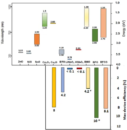
One of the main problem for FEOs absorbers is the high bandgap found for most of these materials. As discussed earlier, an optimal gap of 1.34 eV is the target for an optimal matching with the solar spectra and to approach a high efficiency device. Bismuth Ferrite based oxide, one of the most studied material for Ferroelectric solar cell, shows instead a gap of 2.7 eV. The mechanism will be further discussed in chapter 2 but the low light absorption did not allow BFO based device to overcome 10% efficiency (fig.1.12).
Figure 1.12. Bandgap and relative device’s efficiency for solar cells51
In Fig.1.13 are reported some of the Inorganic oxide compounds by their bandgap and consequently the expected solar cell-based efficiencies according to SQ limit. The ferroelectric oxides exhibit a strong potential as materials to match the solar spectrum absorption. The recent efficiencies BMO/BMn2O5 come from the possibility to tune the bandgap. The same was done by introducing a controlled amount of Cr within the structure of BFO; this allowed Nechache et al.52 to fabricate for he first time a solar cell with a remarkable 8.1% efficiency. Yet, there are several questions (growth models, order vs disorder, photovoltaic versus ferroelectricity ...) and hopefully solutions which open the route for developing a new type of solar cell that could potentially compete with conventional PV technologies. The present
20 thesis work is intending to contribute to master the synthesis of BFCO films, to get a deep insight on the carriers transport within such oxides and finally to design a FEO solar cell structure with appropriate electrodes for extracting the carriers under sun illumination.
*illuminated by a bandgap wavelength diode #BMO/BMn2O5 device
Figure 1.13.Bandgap of some metal oxides used in Photovoltaic Devices and reported
maximum efficiency of the device
1.3.Summary
In this chapter, we first reported briefly on the principle of photovoltaic effect and discussed some basic principles. Then we presented an overview of the present photovoltaic materials and technologies, ranging from silicon based solar cells to thin films. The best efficiencies as recorded in literature are given and some technical and/or ecological limitations are given. Finally, the metal oxides for photovoltaics were introduced. The potential of ferroelectric oxides as absorbing materials for solar cells was discussed.
The next chapter will focus more deeply on the properties of the perovskite oxide and their potential for photovoltaics conversion.
21
References of Chapter 1:
1. Green, M. A. Solar cells: operating principles, technology and system applications. (Univ. of New South Wales, 1998).
2. Shah, A. Photovoltaic Technology: The Case for Thin-Film Solar Cells. Science 285, 692– 698 (1999).
22 3. Future Energy. (2018). Available at:
https://futurenergyweb.es/en/solar-grows-by-30-in-2017-with-demand-set-to-rise-over-next-5-years/.
4. PVeducation. (2018). Available at: https://pveducation.org/. 5. Solar cells and their applications. (Wiley, 2010).
6. Bana, S. & Saini, R. P. A mathematical modeling framework to evaluate the performance of single diode and double diode based SPV systems. Energy Rep. 2, 171–187 (2016). 7. Shockley, W. & Queisser, H. J. Detailed Balance Limit of Efficiency of p‐n Junction Solar
Cells. J. Appl. Phys. 32, 510–519 (1961).
8. Byrnes, S. The Shockley-Queisser Limit and its Discontents. (2015). Available at: http://sjbyrnes.com/shockley_queisser_talk.pdf. (Accessed: 25th September 2018) 9. Ibn-Mohammed, T. et al. Perovskite solar cells: An integrated hybrid lifecycle assessment
and review in comparison with other photovoltaic technologies. Renew. Sustain. Energy
Rev. 80, 1321–1344 (2017).
10. NREL best efficiency. (2018). Available at: https://www.nrel.gov/pv/. (Accessed: 28th June 2018)
11. Jackson, P. et al. Properties of Cu(In,Ga)Se 2 solar cells with new record efficiencies up to 21.7%: Properties of Cu(In,Ga)Se 2 solar cells with new record efficiencies up to 21.7%.
Phys. Status Solidi RRL - Rapid Res. Lett. 9, 28–31 (2015).
12. Shin, B. et al. Thin film solar cell with 8.4% power conversion efficiency using an earth-abundant Cu 2 ZnSnS 4 absorber: Cu 2 ZnSnS 4 solar cell with 8.4% efficiency. Prog.
Photovolt. Res. Appl. 21, 72–76 (2013).
13. Wang, W. et al. Device Characteristics of CZTSSe Thin-Film Solar Cells with 12.6% Efficiency. Adv. Energy Mater. 4, 1301465 (2014).
14. Yoshikawa, K. et al. Silicon heterojunction solar cell with interdigitated back contacts for a photoconversion efficiency over 26%. Nat. Energy 2, 17032 (2017).
15. Jackson, P. et al. New world record efficiency for Cu(In,Ga)Se2 thin-film solar cells beyond 20%. Prog. Photovolt. Res. Appl. 19, 894–897 (2011).
16. Matsubara, H., Tanabe, T., Moto, A., Mine, Y. & Takagishi, S. Over 27% efficiency GaAs/InGaAs mechanically stacked solar cell. Sol. Energy Mater. Sol. Cells 50, 177–184 (1998).
17. Li, M. et al. Solution-processed organic tandem solar cells with power conversion efficiencies >12%. Nat. Photonics 11, 85–90 (2017).
18. Gresser, R., Hummert, M., Hartmann, H., Leo, K. & Riede, M. Synthesis and
Characterization of Near-Infrared Absorbing Benzannulated Aza-BODIPY Dyes. Chem. -
Eur. J. 17, 2939–2947 (2011).
19. Kraner, S. et al. Influence of side groups on the performance of infrared absorbing aza-BODIPY organic solar cells: Performance of IR absorbing aza-aza-BODIPY organic solar cells.
Phys. Status Solidi A 212, 2747–2753 (2015).
20. Bisquert, J. Nanostructured energy devices: foundations of carrier transport. (CRC Press, Taylor & Francis Group, 2018).
21. Li, C., Liu, M., Pschirer, N. G., Baumgarten, M. & Müllen, K. Polyphenylene-Based Materials for Organic Photovoltaics. Chem. Rev. 110, 6817–6855 (2010).
22. Clarke, T. M. & Durrant, J. R. Charge Photogeneration in Organic Solar Cells. Chem. Rev.
110, 6736–6767 (2010).
23. Hains, A. W., Liang, Z., Woodhouse, M. A. & Gregg, B. A. Molecular Semiconductors in Organic Photovoltaic Cells. Chem. Rev. 110, 6689–6735 (2010).
23 24. Chu, T.-Y. et al. Bulk Heterojunction Solar Cells Using Thieno[3,4- c ]pyrrole-4,6-dione
and Dithieno[3,2- b :2′,3′- d ]silole Copolymer with a Power Conversion Efficiency of 7.3%. J. Am. Chem. Soc. 133, 4250–4253 (2011).
25. Peter, L. M. The Grätzel Cell: Where Next? J. Phys. Chem. Lett. 2, 1861–1867 (2011). 26. Yella, A. et al. Porphyrin-Sensitized Solar Cells with Cobalt (II/III)-Based Redox Electrolyte
Exceed 12 Percent Efficiency. Science 334, 629–634 (2011).
27. He, F. & Yu, L. How Far Can Polymer Solar Cells Go? In Need of a Synergistic Approach. J.
Phys. Chem. Lett. 2, 3102–3113 (2011).
28. Sanehira, E. M. et al. Enhanced mobility CsPbI 3 quantum dot arrays for record-efficiency, high-voltage photovoltaic cells. Sci. Adv. 3, eaao4204 (2017).
29. Kojima, A., Teshima, K., Shirai, Y. & Miyasaka, T. Organometal Halide Perovskites as Visible-Light Sensitizers for Photovoltaic Cells. J. Am. Chem. Soc. 131, 6050–6051 (2009). 30. Liu, M., Johnston, M. B. & Snaith, H. J. Efficient planar heterojunction perovskite solar
cells by vapour deposition. Nature 501, 395–398 (2013).
31. Jeon, N. J. et al. Compositional engineering of perovskite materials for high-performance solar cells. Nature 517, 476–480 (2015).
32. Ren, Y. et al. A Stable Blue Photosensitizer for Color Palette of Dye-Sensitized Solar Cells Reaching 12.6% Efficiency. J. Am. Chem. Soc. 140, 2405–2408 (2018).
33. Yang, W. S. et al. Iodide management in formamidinium-lead-halide–based perovskite layers for efficient solar cells. Science 356, 1376–1379 (2017).
34. Mori, S. et al. Organic photovoltaic module development with inverted device structure.
MRS Proc. 1737, (2015).
35. Lorenz, M. et al. The 2016 oxide electronic materials and oxide interfaces roadmap. J.
Phys. Appl. Phys. 49, 433001 (2016).
36. Chen, Y. Z. et al. A high-mobility two-dimensional electron gas at the spinel/perovskite interface of γ-Al2O3/SrTiO3. Nat. Commun. 4, 1371 (2013).
37. Xu, X., Randorn, C., Efstathiou, P. & Irvine, J. T. S. A red metallic oxide photocatalyst. Nat.
Mater. 11, 595–598 (2012).
38. Padmavathy, N. & Vijayaraghavan, R. Enhanced bioactivity of ZnO nanoparticles—an antimicrobial study. Sci. Technol. Adv. Mater. 9, 035004 (2008).
39. Iwanowski, R. J. & Trivich†dr, D. Enhancement of the photovoltaic conversion efficiency in Cu/Cu2O schottky barrier solar cells by H+ ion irradiation. Phys. Status Solidi A 95, 735–741 (1986).
40. Herion, J., Niekisch, E. A. & Scharl, G. Investigation of metal oxide/cuprous oxide heterojunction solar cells. Sol. Energy Mater. 4, 101–112 (1980).
41. Minami, T., Nishi, Y. & Miyata, T. Heterojunction solar cell with 6% efficiency based on an n-type aluminum–gallium–oxide thin film and p-type sodium-doped Cu 2 O sheet. Appl.
Phys. Express 8, 022301 (2015).
42. Rühle, S. et al. All-Oxide Photovoltaics. J. Phys. Chem. Lett. 3, 3755–3764 (2012). 43. Koffyberg, F. P. & Benko, F. A. A photoelectrochemical determination of the position of
the conduction and valence band edges of p ‐type CuO. J. Appl. Phys. 53, 1173–1177 (1982).
44. Hong, M.-J., Lin, Y.-C., Chao, L.-C., Lin, P.-H. & Huang, B.-R. Cupric and cuprous oxide by reactive ion beam sputter deposition and the photosensing properties of cupric oxide metal–semiconductor–metal Schottky photodiodes. Appl. Surf. Sci. 346, 18–23 (2015).
24 45. Ray, S. C. Preparation of copper oxide thin film by the sol–gel-like dip technique and
study of their structural and optical properties. Sol. Energy Mater. Sol. Cells 68, 307–312 (2001).
46. Dimopoulos, T. et al. Photovoltaic properties of thin film heterojunctions with cupric oxide absorber. J. Renew. Sustain. Energy 5, 011205 (2013).
47. Wang, P., Zhao, X. & Li, B. ZnO-coated CuO nanowire arrays: fabrications, optoelectronic properties, and photovoltaic applications. Opt. Express 19, 11271 (2011).
48. Bhardwaj, R., Barman, R. & Kaur, D. Improved photovoltaic effect in CuO/Zn1−xMgxO heterojunction solar cell by pulsed laser deposition. Mater. Lett. 185, 230–234 (2016). 49. Lira-Cantu, M. The Future of Semiconductor Oxides in Next-Generation Solar Cells.
(2017).
50. Spanier, J. E. et al. Power conversion efficiency exceeding the Shockley–Queisser limit in a ferroelectric insulator. Nat. Photonics 10, 611–616 (2016).
51. Zhang, J. et al. Enlarging photovoltaic effect: combination of classic photoelectric and ferroelectric photovoltaic effects. Sci. Rep. 3, (2013).
52. Nechache, R. et al. Bandgap tuning of multiferroic oxide solar cells. Nat.Photonics 9, 61- 67 (2014)
Chapter 2.
25 There are several types of oxide materials that differentiates often by the number of cations, which results in different structures and compositions. The most typical structure of complex or mixed oxides consists simply in two or more different cations with different oxidation states, ionic radii and coordination numbers. This diversity creates a large variety of complex structures which reflects on different properties of these oxides. Among the most known structures are the spinel structures (AB2O4) which are well considered for their magnetic properties. In the most typical case, the A site is a six-folded coordinated ion while a sixfold-coordinate cation occupies the B-site. Eventually, in the most complex cases, a mixing of ion and cation in the A and B site occurs. For this reason, these materials result in a large variety of complex structures and different properties. In this chapter, we will report on oxide compounds, especially those with perovskite crystallographic structure, looking to their characteristics and how they can find application in photovoltaics.
2.1. Structure of perovskite oxides
Perovskites are a family of materials with typical chemical composition ABO3 where A and B are two different cations. They were named so after the discovery of the first crystal, CaTiO3, in Ural Mountains in Russia. The chemical composition is similar to that of the ilmenite: in the ilmenites the A and B atoms are approximately of the same size (e.g. LiSbO3) and occupy the octahedral site. Yet, ilmenites have different structures as compared to the perovskite ones. The family of Perovskites evolves a large number of structures. A typical structure consists in a large cation on the A site that is 12 coordinate and a smaller 6 coordinated ion on the B site. As shown in figure 2.1, the ideal perovskite is a cubic lattice. However, due to different atoms that can take part in the structure, most of the perovskite compounds are distorted and presents a lower symmetry (e.g. orthorhombic or hexagonal), or just a slight distortion from the perfect cubic lattice.
26 .
FIG.2.1. Simple cubic double perovskite with general formula ABX3, A is the cation surrounded by a network of corner-sharing BX6 octahedra1
The deviation from the ideal structure is estimated through a factor of tolerance t which is taken out from the perovskite oxide ABO3 regarded as a purely ionic. In this way, the relation between the radii of the A atom, the B atom and the Oxygen is:
rA+rO=√𝟐 (rB+rO) (eq. 2.1)
It is then possible to express the deviation from the ideal cubic structure by tIR 2: tIR= (rA+rO)/ √𝟐(rB+rO) (eq.2.2)
The tolerance factor for maintaining a perovskite structure should be between 0.80 and 1.10. For smaller or larger t, the same compound would turn to the ilmenite structure.
In fig.2.2 are shown all the chemical elements which can form a perovskite structure. As can be seen, most of the elements, except the noble gases and few others, can form a perovskite. The stability of these structures relies not only on the ratio between the A and the B atoms but even on their nature. In fact, for the B atom, the bonds are highly covalent. In this sense, is not surprising that an oxide such as BaGeO3 does not fit the perovskite structure in ambient condition, as the preferred coordination number for Ge is 4. An alternative is to form a perovskite BaGeO3 structure by high pressure synthesis, as higher Ge coordination number starts to be preferred 3.
27
Fig.2.2. A map of the elements which occupy the A, B, and/or X sites within the 576
compounds experimentally characterized as perovskite or non-perovskite at ambient conditions and reported in 4–6. The data set spans 77 elements, with 49 elements appearing
at the A site, 67 at the B site, and 5 at the X site.
It is clear that the perovskite structure can be formed by a great number of atoms and therefore many materials are reported. In the table below are given some of them which exhibit different numbers of oxidation, consequently affecting the crystallographic structure as well as the quantity of oxygen related defects and therefore the final properties. The table gives the ideal A-O, B-O bond distances (dA-O; dB-O) and the ionic radii for several oxides.
Perovskites in A3+B3+O 3
d A-O (Å) d B-O (Å) Tolerance factor
(t) BiFeO3 2.607 2.015 0.915 GdFeO3 2.578 2.015 0.904 LaAlO3 2.685 1.876 1.012 DyScO3 2.514 2.105 0.844 NdGaO3 2.618 1.986 0.932 BiMnO3 2.607 2.016 0.914
28
Perovskites in A2+B4+O 3
d A-O (Å) d B-O (Å) Tolerance factor
(t) BaTiO3 2.948 1.965 1.061 SrRuO3 2.781 1.984 0.991 SrTiO3 2.781 1.965 1.001 PbTiO3 2.775 1.965 0.999 CaTiO3 2.630 1.965 0.964 Perovskites in A+B5+O 3
d A-O (Å) d B-O (Å) Tolerance factor
(t)
KNbO3 3.051 1.971 1.091
NaWO3 2.722 1.975 0.983
KUO3 3.051 2.142 1.007
Table 2.1.Ideal A-O, B-O bond distances and ionic radii calculated tolerance factor (t) for
different perovskites of A3+B3+O3 group, A2+B4+O3 group and A+B5+O3 group respectively 4
2.2. Typical properties of perovskite oxides
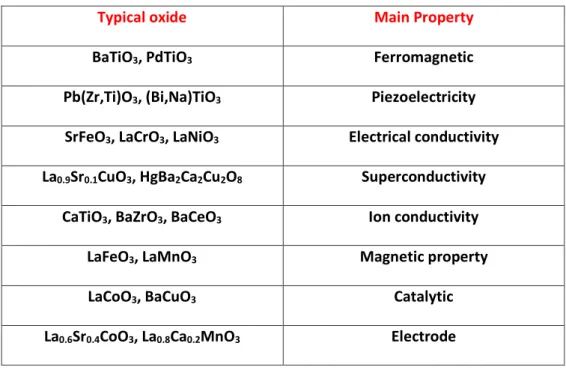
As it has been mentioned above, the perovskite oxides can show a large variety of chemical composition and a variety of structures. It is thus not surprising to find that they possess a large number of properties and different applications. There are some applications which have been known since a long time such as ferroelectricity which can be considered somehow the stone of these family of perovskites. This is for instance the case for BaTiO3. Another well-known property is the superconductivity like for YBa2Cu3O7. Table 2.2 summarizes the main applications of some of the most known perovskites.
29
Typical oxide Main Property
BaTiO3, PdTiO3 Ferromagnetic
Pb(Zr,Ti)O3, (Bi,Na)TiO3 Piezoelectricity
SrFeO3, LaCrO3, LaNiO3 Electrical conductivity
La0.9Sr0.1CuO3, HgBa2Ca2Cu2O8 Superconductivity
CaTiO3, BaZrO3, BaCeO3 Ion conductivity
LaFeO3, LaMnO3 Magnetic property
LaCoO3, BaCuO3 Catalytic
La0.6Sr0.4CoO3, La0.8Ca0.2MnO3 Electrode
Table 2.2.Typical properties of perovskite oxides and some examples7
2.3. The double perovskite
Cation substitution is one of the ways to tune the properties of the perovskite oxide compound. The cation can take place both at A or B site and it can involve different amount of substitution. In the case of a substitution of half of the B site with a different cation, there is a possibility of ordered growth double perovskite of composition A2B’B’’O6 where B’ and B’’ are the two different cations at the B site. A schematic representation of the double perovskite is given in fig.2.3.
The alternation of B and B’ cations allow the creation of ordered or disordered structures, adding a degree of complexity in the structure and properties of these compounds, that can be engineered to obtain the desired properties.
30
Fig.2.3. A2BB’X6, in the rock salt double perovskite structure where the A cations are surrounded by an alternating network of BX6 and B’X6 octahedra8.
2.3.1 Ordering in double perovskite
The degree of order or disorder inside the double perovskite is of great importance as it controls many of the final properties of the resulting material. For example, the degree of order inside Sr2FeMoO6 strongly affects the magnetoresistance as well as the half-metallic properties of the film.9,10 . Most of the double perovskites crystallize with a rock-salt order (more than 650 compounds have been reported to grow in this way) or just disordered (100 compounds). A third possibility of ordering resides on a “layered” order. It has been postulated that this type of order is only possible in a very narrow range of balancing properties: only 5 compounds have been reported to crystallize in this way11–13 . The disorder inside the double perovskite can occur in different ways. The most common one is the antisite (AS) disorder, in which one cation just takes the place of the other inside the crystal structure. This type of order’ defects happens mostly during the crystal growth because of the configurational entropy. Another common type of defect is the anti-phase boundary (APB). In this case, two ordered zone are divided by two inverted B’ and B’’ sites.
31
Fig.2.4. B-site cation disorder schemes: (a) completely ordered, (b) antisite disorder and (c)
antiphase boundary. 14
Since the ordering inside the double perovskite is essential for their applications, is important to understand how to study it. Most often, the study of ordering inside the double perovskite is done by diffraction analysis. The ordering and the doubling of the cell generate superstructures peaks which can be easily detected. On the other hand, because of distortion, octahedron tilting and cation ordering can make the results vary. Moreover, if B’ and B’’ are cations with close number of electrons, it can cause other difficulties in the ordering studies, and consequently it will be hard to distinguish between the two atoms. These problems have already been found in some double perovskite like La2NiMnO6 15, Ba2RTaO6 16 ( R= lanthanide) and in some compounds in which B’ and B’’ have the same number of electrons like A3+2Ca2+Ti4+O6; A2+2Sc3+V5+O6 17,18.
The degree of order inside the crystal depends on several factors and it’s not straightforward to understand whether the film would crystallize in an ordered or disordered way. In fact, most of these compounds are expected to be highly disordered, as a first approximation, at least for energetic consideration19. Surprisingly however, many reports on these compounds show that they crystallize in a highly ordered state. One of the suggested reasons of ordering inside the double perovskite lies on the B-site cation’ difference oxidation state, ΔZB=|ZB’’-ZB’|, where Z is the oxidation state of the B cation. Generally speaking, it is possible to say that when ΔZB<2, the compounds crystallize in a disordered way, while if ΔZB>2 the compounds are ordered 4,10,20–22. Qualitatively speaking, it is possible to explain this effect by an unfavourable situation while placing two high charged B cations one close to the other. More specifically, a high increment of the Madelung energy (which calculates the electrostatic repulsion of an ion in a crystal by approximating the ion to a point charge) 23 is caused
32
by an increased charge difference24. It has been calculated that the Madelung energy ordering is proportional to ΔZB2 which means that the ordering energy can become really important by a small change in the oxidation state. In that case, the repulsion energy overcomes easily the entropic energy and the crystal orders during the growth.25,26
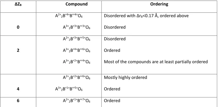
The second common reason that provokes cation order is the difference in the radius between the cations. The more is the difference, which reflects in a larger factor ΔrB=|rB’’-rB’| (where r is the radius of the B cation), the more probable is the ordered growth of the crystal. Making the similar assumption as before, it is possible to consider that larger is the difference ΔrB, more easily the lattice strain can overcome the entropic energy and so the cations are ordered. 26 The effect of ordering by changing the ionic radius of the two cations has been calculated in some different compounds containing M3+/Nb5+ by Galasso and Darby in 1962 27. From their work, it has been established that a difference in the radii higher than 7% is already enough for cationic ordering. Vasala and Karpinnen, in their double perovskite review14, summarized the ordering of the double perovskite by ionic radii as follows:
ΔZB Compound Ordering 0 A2+ 2B’4+B’’4+O6 A3+ 2B’3+B’’3+O6
Disordered with ΔrB<0.17 Å, ordered above Disordered 2 A2+ 2B’3+B’’5+O6 A3+ 2B’4+B’’6+O6 A3+ 2B’2+B’’4+O6 Disordered Ordered
Most of the compounds are at least partially ordered
4
A2+
2B’2+B’’6+O6 A3+
2B’1+B’’5+O6
Mostly highly ordered Ordered
6 A2+
2B’1+B’’7+O6 Ordered
Table 2.3. Ordering of known double perovskite by the difference of the oxidation state of B’ and B’’
33
2.4. Multiferroic perovskite oxide for Photovoltaics
As mentioned above some of the perovskite oxides can exhibit ferroelectric and ferromagnetic properties that can be interesting for the photovoltaic conversion. Before developing further, let’s remind some basics of ferroelectricity, ferromagnetisms and finally multiferroicity effects.
2.4.1. Ferroelectricity
Ferroelectricity is a property that some materials have for which their spontaneous polarization can be switched by an external electric field. A ferroelectric (FE) material will remain polarized even if the external field is removed. Moreover, this polarization can be switched by applying a field larger than critical values (which depend on the materials) called coercive field, Ec. Fig. 2.5 shows a typical curve of polarization versus the electric field for a ferroelectric material. It is possible to distinguish between the thresholds for the coercive field, the remnant polarization and the saturated polarization.
FiG.2.5. Typical curve of Polarization vs the Electric field for a Ferroelectric material. It is
possible to distinguish between the Remnant polarization (Pr), the saturated Polarization (Ps) and the coercive field (Ec)28
The first discovery of this effect was made in 1921 in single-crystal materials (called Rochelle salt) and subsequently in other materials like perovskite ones (BaTiO3 (BTO) in 1940). In perovskites, 2 phases are possible: the paraelectric one when the crystal is centro-symmetric
34 and the ferroelectric one where the atoms are displaced along a specific direction showing a net dipole moment which responds to an external polarization. This shifting can occur for different causes. In the case of BFO, as an example, it occurs because the Bismuth in the perovskite structure presents a lone pairs (valence pair of electrons not shared with another atom) on the outer shell of the atom, which are high sensitive to the polarization.
2.4.2. Ferromagnetism
Ferromagnetism is a mechanism where an uncharged material forms permanent magnets. It is given by a certain number of atoms whose spins are aligned one to each other so that they create a net magnetic moment. Different types of magnetism are known in physics: Ferromagnetism and ferrimagnetism are the strongest types and are the most noticeable phenomena that are encountered in mostly everyday life. Other substances respond weakly with another type of magnetism, called paramagnetism, diamagnetism and antiferromagnetism. In fig.2.6 are shown the spins’ orientations in each case.
FiG.2.6. Spins representation in different material: a) Ferromagnetic; b) Paramagnetic; c)
Antiferromagnetic; d) Ferrimagnetic
Figure 2.6 a shows a ferromagnetic effect, which has been already discussed. In figure 2.6 b a paramagnetic effect is shown; in this case, the material is weakly attracted by an external magnetic field and forms a little induced internal magnetic field as its spins tends to align to the external field. When the atom’s spins are ordered antiparallel and can cancel each other there will be an antiferromagnetic order like in figure 2.6 c; when the order is antiferro but
35 the spin are not sufficient to cancel each other there is a ferrimagnet behaviour as in figure 2.6 d.
2.4.4. Multiferroicity
Multiferroics are a class of materials which shows at least two of the three order parameter (electrical, magnetical and mechanical) at the same time29–31. These type of materials, in which it would be for example possible to control magnetism and coupling are of strong interest for different potential application 32–34. Fig.2.7 gives examples of multiferroic behavior.
Most of the compounds known which show a Multiferroic behaviour have a Curie temperature well below room temperature. The Curie temperature is the temperature at which a ferroelectric material loses its ferroelectric behaviour and starts to act as a paramagnetic one. For example, these MF materials have been investigated for tunnelling magnetoresistance (TMR) sensors or magnetic memories applications, which can in the late case be written electrically and read magnetically.
FiG.2.7. Summary of all the functionalities that multiferroic materials may offer. E and P
stand for electric field and electric polarization, H and M stand for magnetic field and magnetization, and σ and εstand for stress and deformation, respectively35
It is generally difficult to obtain a multiferroic material since there are severe restrictions on the synthesis 30. Therefore, most of them are complex oxide, as shown in fig. 2.8.
36 Thus, BiFeO3 (BFO) 33 is a perovskite which has been studied for years since it exhibits ferroelectricity (Tc= 1083 K) 36 and ferromagnetism ( TN= 683 K) 37 at room temperature. Other compounds have been synthesized and demonstrated to have multiferroicity in this condition. Perovskites like BaTiO3 38 or compounds like KBBNO 39 have also shown promising properties. Among other oxides present at the interface of the red and green circles, there is the double perovskite Bi2FeCrO6 (or BFCO) that has attracted a great interest for several reasons which will be discussed below. For instance, Nechache et al.40 were able to exploit this material for Photovoltaic (PV) applications to get an unprecedent high solar conversion efficiency of 8.1%.
Fig.2.8: In the large circle are represented the insulating oxides of interest; within them
there are those polarizable (green ellipse) and magnetically polarizable (orange ellipse). Inside the insert circles, depending on the ellipse, there are Ferroelectrics and
Ferro/Ferri-magnets. At the intersections, there are different multiferroics41
2.4.5. The case of BiFeO3 and Bi2FeCrO6
The closer structure to the one of Bi2FeCrO6 (labelled often BFCO) is BiFeO3 (labelled BFO). The structure of BFO is characterized by two distorted perovskite which are connected along diagonal or the pseudocubic [111] direction, to build a rhombohedral unit cell. In this structure, the two oxygen octahedra of the cells connected along the [111] direction are rotated clockwise and counterclockwise around the [111] direction by ± 13.8° and the Fe-ion is shifted by 0.135 Å along the same axis away from the oxygen octahedron center position.
37 The reported lattice parameter are of a= 3.965 Å and a rhombohedral angle of α = 89.3°. The perovskite can be even described as a hexagonal structure with the c-axis parallel to the diagonals of the perovskite cube; in this case it will be: [001]hex//[111]pseudocubic and , the lattice parameters would be ahex = 5.58 Å and chex = 13.89 Å. It has been pointed out that BFCO is isostructural to BFO (fig.XX)
Fig.2.9. Schematic representation of BFCO double perovskite. From42
In fact, the Bi2FeCrO6 structure can be described by a R3 symmetry (the theoretical lattice parameters for the rhombohedral structures: arh = 0.547 nm; αrh = 60.09°). This structure can also be approximated by a pseudo-cubic one. As shown in Fig.4.5, it is possible to see the double perovskite both as a pseudo-cubic and hexagonal. By the approximation to a pseudo cubic structure, it is possible to understand why BFCO grows in a 4-folded structure.
Figure 4.5. Sketch of the crystalline structure of BFCO which underlines the equivalency of
the hexagonal and pseudo-cubic notification. The black lines are meant to visually enhance the structure.
38 It has been predicted to bring, in this long-range order configuration, a magnetic moment of 2 µB per formula unit (ca.160 emu/cm3) at 110K and a ferroelectric polarization of 80 µC/cm2. It is well known that in order to have a multiferroic material, the two ferroic orders should be brought from 2 different atoms in the crystalline structure.
For BFCO, the ferroelectricity is due to the 6s2 lone pairs of the Bi3+ atoms (like in BiMnO3 or BiFeO3) while the ferromagnetism is linked with Fe3+ and Cr3+ ordering inside the crystal. Taking into account the Kanamori-Goodenough rules43,44, ferromagnetism appears when:
• Two transition metal (TM) are ordered in a B’-O-B’’ rocksalt structure • One of these two TM presents eg electrons while the other don’t.
In the case of BFCO, a Fe3+ with configuration t2g3eg2 coupled with a Cr3+ that presents a configuration t2g3eg0 should produce a ferromagnetic crystal, while a coupling between Fe-Fe and Cr-Cr should results in antiferromagnetic coupling. This effect was well described by Villafuerte-Castrejon et al.45 A schematic representation of magnetic domains in the BFCO crystal is given in fig.2.10.
Fig.2.10. Representation of magnetic domains in the crystal, linked to Fe3+and Cr3+ position45 From the synthesis point of view, Bi2FeCrO6 is not likely to grow along a specific order as the two atoms in B’ and B’’ position have similar ionic radii and are most stable in the same oxidation state (Fe3+= 0.645 Å; Cr3+=0.615 Å). As mentioned in section 2.3.1, the BFCO double