HAL Id: hal-01143150
https://hal.archives-ouvertes.fr/hal-01143150
Submitted on 28 Mar 2018HAL is a multi-disciplinary open access archive for the deposit and dissemination of sci-entific research documents, whether they are pub-lished or not. The documents may come from
L’archive ouverte pluridisciplinaire HAL, est destinée au dépôt et à la diffusion de documents scientifiques de niveau recherche, publiés ou non, émanant des établissements d’enseignement et de
Imaging the Fine Structure of a Magnetic Domain Wall
in a Ni Nanocylinder
Nicolas Biziere, Christophe Gatel, Remy Lassalle-Balier, Marie-Claude
Clochard, J.-E. Wegrowe, Etienne Snoeck
To cite this version:
Nicolas Biziere, Christophe Gatel, Remy Lassalle-Balier, Marie-Claude Clochard, J.-E. Wegrowe, et al.. Imaging the Fine Structure of a Magnetic Domain Wall in a Ni Nanocylinder. Nano Letters, American Chemical Society, 2013, 13, pp.2053-2057. �10.1021/nl400317j�. �hal-01143150�
Imaging the fine structure of a magnetic domain wall
in a Ni nano-cylinder.
Nicolas Biziere,†* Christophe Gatel, † Rémy Lassalle-Balier, $ Marie Claude Clochard, ‡ Jean Eric Wegrowe, ‡ and Etienne Snoeck†
† CEMES-CNRS, 31055, Toulouse, France
$ School of Physics and CRANN/Trinity College, Dublin 2, Ireland ‡ LSI/CEA/CNRS/Ecole Polytechnique, 91128 Palaiseau, France
KEYWORDS Magnetic domain wall, electron holography, magnetic transition, 3D nanomagnetism
ABSTRACT : We present the first experimental imaging of the internal DW structure in 55 nm
and 85 nm diameters Ni nano-cylinders, using electron holography combined with micromagnetic calculations. We demonstrate the magnetic transition from a hybrid magnetic state with both vortex and transverse DW in 85 nm diameter Ni nano-cylinders to a pure transverse wall in thinner nanowires. This is particularly important as DWs in nano-cylinders are model systems to go beyond the classical Walker limit.
Keywords : magnetic domain walls, electron holography, nano-cylinder, 3D micromagnetism.
The determination of the shape of domain walls (DW) in magnetic nano-cylinders has become a very important topic in magnetism both for theoretical and technological issues. Indeed magnetic nano-cylinders are expected to show a magnetic transition from vortex to transverse wall as the diameter is reduced1,2, reflecting the competition between dipolar and exchange energy. Moreover, their cylindrical symmetry prevents any change in the demagnetizing energy as the spins rotate during propagation3,4 and should led to a suppression of the Walker breakdown5-7. This has been predicted in particular in the case of a transverse wall in a nano-cylinder. The latter point is of particular interest for technological applications such as logic circuit or data storage8-10, manipulating the walls by means of magnetic fields11-14 or electric current15-19, and for which the Walker breakdown is the main limitation on the DW velocities. Imaging and understanding the fine structure of the DW in nano-cylinders is then of major importance to make these systems an interesting alternative to the usual flat nanostripes produced by lithography.
While magnetic DW have been almost exclusively studied experimentally in nano-stripes, most of the research on nano-cylinders has been carried out by means of micromagnetic calculations
and very few experimental studies of these structures have been performed up to now20,21. There are two major issues. The first is the difficulty to grow cylindrical magnetic nanostructures of good quality and the second is the difficulty of studying the DW structure inside the object with sufficient spatial resolution. We bypass these two limitations by using template synthesis to grow high quality Ni nano-cylinders and we use high spatial resolution off-axis electron holography to study the magnetic configuration of the DW. The internal structure of the DW is recovered comparing the experimental magnetic phase shift image of the electrons beam with the one calculated from micromagnetic simulations, taking into account the structural properties of the
wire deduced from the TEM studies. As the electron cross the whole sample, electron holography offers direct information on the internal magnetic structure with a spatial resolution of about 5 nm as compared to other techniques such as MFM, for which the magnetic state is observed via its stray field, or MOKE or SEMPA22-24 which are sensitive to surface magnetization and present spatial resolution of few tens of nm. Moreover, as compared to previous electron holography experiments on nano-cylinders (ref 21) showing the stray field of the DW, we optimize the observation condition (see below) to study at higher magnification the magnetic state inside the wire.
Ni nano-cylinders with diameters around 80 nm ± 25 nm are grown by electro deposition in commercial 6 µm thick polycarbonate membranes25-27. The membranes are then dissolved in CH2Cl2 and the Ni nanowires are recovered on a carbon foil for structural and magnetic TEM
imaging. Figure 1a shows a TEM image of one of these Ni nanowires of about 90 nm in diameter with its corresponding diffraction pattern in Figure 1b. They both clearly demonstrate the polycrystalline structure of the wire with randomly oriented grains, leading to a random distribution of crystalline anisotropy and grain sizes roughly equal to the wire diameter.
Figure 1. (a) TEM images of Ni nano-cylinders grown by electrodeposition. Triangular shape
crystalline domains are observed revealing a randomly distributed crystal orientation.. (b) Diffraction
pattern of the same area presented in (a).
Off-axis electron holography experiments performed in a spherical aberration-corrected Tecnai
F20 microscope are used to image the remanent magnetic configuration of single nano-cylinders. Electron holography allows recovery of the phase of the electron beam that has been modified by interaction with magnetic and electrostatic fields inside and outside a nanostructure. The magnetic and the electrostatic contributions to the total phase shift are separated by subtracting two holograms where the sample has been inverted28 (see supplementary). The magnetic phase shift can then be written as :
where z is the direction of the electron beam (perpendicular to the wire axis), r is a direction perpendicular to z and B┴ is the amplitude of the magnetic induction perpendicular to both r and
z. The isophase contour of the phase image then gives a direct representation of the projected
induction field lines. However, as the phase shift is integrated over the entire path of the electron, the 2D recorded image contains all the information about the internal structure of the domain wall projected along the z direction.
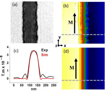
Before imaging at the remanence, a 2 Tesla magnetic field was applied perpendicular to the nanowire axis (same direction than the electron path) using the electromagnetic objective lens of the microscope. We apply the field perpendicularly to the wire axis in order to favor transverse walls nanowires of smallest diameter. Then a single nanowire lying far from its neighbors is chosen in order to avoid magnetic interaction between them. We present in Figure 2a and 2b the amplitude image and magnetic phase image obtained from a 70 nm diameter Ni nano-cylinder and few microns long in an area where no DW shows up. The induction field lines corresponding to the magnetic isophase contours are plotted inside the wire. They run parallel to the wire axis meaning that the magnetization is uniformly aligned along the wire, without any stray field visible at this scale. This is the simplest magnetic configuration in such 1D structure as the shape anisotropy stabilizes the magnetization along the long axis. Figure 2c and 2d report respectively a quantitative analysis of the amplitude of the projected induction field and the magnetic phase shift calculated for a uniform magnetic state (see details below). We observe a very good quantitative agreement between the experiment and the simulation. The small oscillations of the intensity in the magnetic induction profile on the edge of the wire come from the Fourier filtering used to reconstruct the phase images. This demonstrates the capabilities of electron holography
coupled with micromagnetic simulations to obtain quantitative mapping of magnetic states in nanowires.
Figure 2: Magnetic phase shift of a uniformly magnetized nano-cylinder. Amplitude (a) and (b)
magnetic phase shift images in a piece of nano-cylinder of 70 nm in diameter without DW. The lines in (b) corresponds to the isocontour of the phase shift and then to the induction field lines. (d) Calculated magnetic phase shift and isocontour from micromagnetic simulation. The isophase lines in (b) and (d) are separated by 0.6 rad. (c) Profile of the modulus of the projected induction in the cross section delimited by the dashed line in (b) and (d).
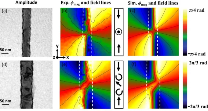
In contrast we show in Figure 3b and 3e the experimental magnetic phase shift image induced by DWs appearing in two nano-cylinders of 55 and 85 nm diameter. Magnetic domain walls are evidenced by the stray field leaking outside the wire in each side of the DWs. Inside the wire, the magnetic flux at the DW position is found to be asymmetric as compared to the uniform case. Moreover, two different DW structures are found for two wires of different diameters. For the
smaller one (Figure 3b), field lines are symmetric with respect to both the X and Y axis and no magnetic induction is observed at the very center of the domain wall. It indicates that the magnetization at this location is either parallel to the + Z or – Z direction (the electron phase shift is only sensitive to the Bx and By components perpendicular to the e- beam). This is the magnetic configuration expected for a pure transverse wall with the spins pointing in the direction of the saturation field (+Z). For the larger diameter wire (Figure 3e), the situation is different. Field lines are symmetric with respect to a (X,Y) plane tilted at about 45° from the Y direction. Once again it indicates that the spins within this plane are pointing in the ±Z direction. Note that such a magnetic DW configuration does not correspond to a vortex state as in such a case, the magnetic flux should be confined within the wire, with a perfect symmetry around the Y axis and no stray field should be observed.
magnetic phase shift and corresponding induction field lines. (c) and (f) Magnetic phase shift and corresponding induction field lines calculated from micromagnetic simulation. The difference of isophase contour is the same for the experiment and simulation, showing the quantitative agreement, and is set to 0.6 rad and 0.3 rad for 55 and 85 nm respectively. The color bars on the right give the amplitude of the phase shift in radian. The dashed lines are a guide for the eye to position the wires. The arrows on the scheme represent a simplified view of the magnetization within the wire.
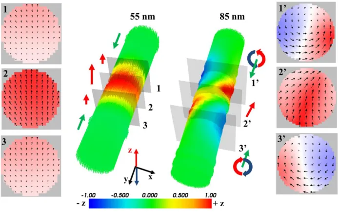
For a better understanding of these magnetic states, micromagnetic 3D calculations have been performed using the OOMMF code29 to map the DW configuration for the two wires. To fit the electron holography experiments, we have calculated the electron beam phase shift images induced by the resulting magnetic state in the whole (X, Y, Z) space. The nanowire diameters used for calculation were deduced from the TEM amplitude images. As for the experiment, in the micromagnetic calculations, the magnetization is first saturated in the +Z direction (perpendicular to the wire axis) applying a magnetic field of 1 Tesla. The polycrystalline structure has been implemented in homemade OOMMF script in order to be as close as possible to the real system (see methods for more details). The total area size is 600 x 600 x 4800 nm3 and the unit cell size is 2.5 x 2.5 x 2.5 nm3. The length of the wires was limited to 3.6 µm in order to limit the number of cells. Parameters used for the calculation are µ0Ms = 0.485 T, magnetocrystalline anisotropy constant K1 = -5.7 e-3 J/m3 and exchange constant A = 9 e-12 J/m. From the remanent magnetic configuration we calculated the magnetic induction B = µ0(Hd + M) and deduced the magnetic phase shift from Eq.1 in all the simulated space. Results of the 3D micromagnetic calculations are shown in Figure 4 where only the part including the DW is
reported as the rest of the wire is uniformly magnetized. The color representation depicts only the Mz component of the magnetization. The snapshots show the magnetization orientation in three different planes perpendicular to the wire.
For the 55 nm diameter wire, micromagnetic calculations indicate a head to head transverse wall. The snapshots 1, 2 and 3 show that the spins at the center of the wall are aligned in the +Z direction, which result of the initial saturation of the sample. The corresponding calculated phase shift is reported in Figure 3c and is in very good agreement with the experimental one (Figure 3b). The shape of the field lines at the center of the wall indicates a slight tilt of the spins at the ± X edges of the wire, which point in opposite directions. The qualitative and quantitative agreements between simulation and experiment clearly prove the appearance of a transverse DW in the 55 nm nanowire.
Micromagnetic simulation indicates a more complex head to head DW in the 85 nm diameter wire. Snapshots 1’, 2’ and 3’ in Figure 4 show that at the start (1’) and the end (3’) of the DW, the spins rotate on the edge of the cylinder (as for a vortex) while at the center (2’) the spins are almost aligned parallel to +Z (i.e. in the direction of the saturation field) as for transverse wall. This “pseudo transverse wall” with spins roughly aligned in the +Z direction (red and yellow part in the 3D simulation) however lies at about 45° of the Y axis. The presence of such a “pseudo” transverse wall implies that the cores of the vortices are not centered along the wire axis as observed in 1’ and 3’. It also induces clockwise and anti-clockwise rotation of the vortices on each side of it. As for the 55 nm diameter case, the phase shift calculated from this magnetic state (Figure 3f) is in perfect agreement with the experimental result (Figure 3e). As the cores of
of a magnetic transition in a cylindrical nanostructure from a pure transverse wall to a hybrid magnetic configuration whose fine structure has been clearly elucidated. It is different from previous works18 which showed that for field applied in the direction of the wire axis, a pure vortex state arises for wires diameter above 60 nm. We assume that such hybrid state strongly depends on the magnetic history of the nanostructure. In addition, we performed simulations for diameters up to 110 nm for which this hybrid state persists.
Figure 4. 3D micromagnetic simulations for the 55 and 85 nm diameter nano-cylinders. The
snapshots present the magnetization at the different planes denoted on the 3D picture.
We must emphasize that saturating the magnetization perpendicular to the wire axis does not lead systematically to the pinning of a DW. As already stated, shape anisotropy tends to align all
the spins in the direction of the wire axis to stabilize a uniform magnetic state. We experimentally observed that most (~60%) of the wires are uniformly magnetized and micromagnetic simulations also confirmed it is the most stable configuration since without considering the polycrystalline structure, DW nucleate but move and collapse at the edge of the wire leading to a uniform magnetic state. We then assume that the polycrystalline structure is responsible for the DW pinning most probably on grain boundaries as already reported in stripes30.
In conclusion, we developed a method combining high resolution electron holography with micromagnetism to obtain unprecedented resolution of the 3D structure of DW in a cylindrical ferromagnetic nanowire. We apply our method to demonstrate the occurrence of a magnetic transition at remanence from a transverse wall to a hybrid magnetic state as a function of the nano-cylinder diameter. As transverse walls can be easily nucleated by saturating the sample perpendicular to the wire axis, they are perfect objects to test the massless DW concept which could be an important breakthrough to develop future spintronics devices.
Supporting Information. Description of the different experimental methods used for nanowire
growth, electron holography experiments and 3D micromagnetic calculation of the magnetic phase shift. This material is available free of charge via the Internet at http://pubs.acs.org.
Corresponding Author
The research leading to these results has received funding from the European Union Seventh Framework Programme under Grant Agreement 312483 - ESTEEM2 (Integrated Infrastructure Initiative – I3) and support from SFI/CRANN/NISE.
REFERENCES
1 Hertel, R. & Kirschner, J. Magnetization reversal dynamics in nickel nanowires. Physica B.
343, 206–210 (2004).
2 Porrati, F., Huth, M. Diagram of the states in arrays of iron nanocylinders. Appl. Phys. Lett.
85, 3157-3159 (2004).
3 Yan, M., Andreas, C., Kákay, A., García-Sánchez, F. & Hertel, R. Fast domain wall dynamics in magnetic nanotubes: Suppression of Walker breakdown and Cherenkov-like spin wave emission. Appl. Phys. Lett. 99, 122505 (2011).
4 Yan, M., Kakay, A., Gliga, S., & Hertel, R. Beating the Walker Limit with Massless DomainWalls in Cylindrical Nanowires. Phys. Rev. Lett. 104, 057201 (2010).
5 Schryer, N.L., Walker, L.R. The motion of 180° domain walls in uniform dc magnetic fields. J.
of Appl. Phys. 45, 5406-5421 (1974)
6 Mougin, A., Cormier, M., Adam, J. P., Metaxas, P. J. & Ferré, J. Domain wall mobility, stability and Walker breakdown in magnetic nanowires. Europhys. Lett. 78, 57007 (2007). 7 Koyama, T. et al. Current-induced magnetic domain wall motion below intrinsic threshold triggered by Walker breakdown. Nature Nanotechnology 7, 635-639 (2012).
8 Parking,S.S.P., Hayashi, M., & Thomas, L. Magnetic domain-wall racetrack memory. Science
320, 190-194 (2008).
9 Hayashi, M., Thomas, L., Moriya, R., Rettner, C. and Parkin, S. S. P. Current-controlled magnetic domain-wall nanowire shift register. Science 320, 209-211 (2008).
10 Franken, J. H., Swagten, H. J. M., Koopmans, B. Shift registers based on magnetic domain wall ratchets with perpendicular anisotropy. Nature Nanotechnology 7, 499-503 (2012).
11 Cayssol, F., Ravelosona, D., Chappert, C., Ferré, J. & Jamet, J. P. Domain Wall Creep in Magnetic Wires. Phys. Rev. Lett. 92, 107202 (2004).
12 Nam, C., Jang, Y., Lee, K.S. & Cho, B. K. Characteristics of domain wall pinning and depinning in a three-terminal magnetic Y-junction. Nanotechnology 19, 015703 (2008).
13 Rhensius, J., Heyne, L., Backes, D., Krzyk, S., Heyderman, L. J., Joly, L., Nolting, F. & Kläui, M. Imaging of Domain Wall Inertia in Permalloy Half-Ring Nanowires by Time-Resolved Photoemission Electron Microscopy. Phys. Rev. Lett. 104, 067201 (2010).
14 Muñoz, M. & Prieto, J.L. Suppression of the intrinsic stochastic pinning of domain walls in magnetic nanostripes. Nature Communications 2, 562 (2011).
15 Bocklage, L., Krüger, B., Matsuyama, T., Bolte, M., Merkt, U., Pfannkuche, D. & Meier, G. Dependence of Magnetic Domain-Wall Motion on a Fast Changing Current. Phys. Rev. Lett.
103, 197204 (2009).
17 Koyama, T. et al. Observation of the intrinsic pinning of a magnetic domain wall in a ferromagnetic nanowire. Nature Materials 10, 194–197 (2011).
18 Chauleau, J.Y., Weil, R., Thiaville, A. & Miltat, J. Magnetic domain walls displacement: Automotion versus spin-transfer torque. Phys. Rev. B. 82, 214414 (2010).
19 Tatara, G. & Kohno, H. Theory of current-driven domain wall motion: spin transfer versus momentum transfer. Phys. Rev. Lett. 92, 086601 (2004).20 Otani, Y. et al. Magnetic and Transport Properties of Micron Size Magnetic Participate Arrays Fabricated on a 2D Superconducting Nb Films and Sub-Micron Magnetic Wires. MRS Spring Meeting - Symposium
Magnetic Ultrathin Films, Multilayers, and Surfaces 475, (1997).
21 Beeli, C., Doudin, B., Ansermet, J.-Ph., Stadelmann, P.A. Measurement of the remanent magnetization of single Co/Cu and Ni nanowires by off-axis TEM electron holography.
Ultramicroscopy 67, 143-151 (1997).
22 Hayashi, M., Thomas, L., Rettner, C., Moriya, R., Jiang X. and Parkin, S. S. P. Dependence of
Current and Field Driven Depinning of DomainWalls on Their Structure and Chirality in Permalloy Nanowires. Phys. Rev. Lett. 97, 207205 (2006).
23 Weiler M. et al. Magnetic microstructure and magnetotransport in Co2FeAl Heusler compound thin films. Appl. Phys. Lett. 98, 042501, (2011).
24 Vaz, C.A.F., Lopez-Diaz, L., Klaui, M., Bland, J.A.C., Monchesky, T.L., Unguris, J. & Cui, Z. Observation of a geometrically constrained domain wall in epitaxial FCC Co small disks. J.
25 Biziere, N., . et al. J. E. Synthesis and magnetic reversal of bi-conical Ni nanostructures. J.
Appl. Phys. 110, 063906 (2011).
26 Wegrowe, J.E., Anh Nguyen, Q., Al-Barki, M., Dayen, J.F., Wade, T.L., & Drouhin, H.J. Anisotropic magnetothermopower: Contribution of interband relaxation. Phys. Rev. B 73, 134422 (2006).
27 Carre n- on le , C.E., De La Torre Medina, J., Piraux, L. & Encinas, A. Electrodeposition Growth of Nanowire Arrays with Height Gradient Profiles for Microwave Device Applications.
Nanoletters 11, 2023-2027 (2011).
28 Midgley, P.A. & Dunin-Borkowski R.E. Electron tomography and holography in materials science. Nature Materials 8, 271-280 (2009).
29 M. J. Donahue and D. . Porter, OOMMF User’s uide, http://math.nist.gov/oommf.
30 Nagai, T. et al. Direct observation of the spin structures of vortex domain walls in ferromagnetic nanowires. Phys. Rev. B. 78, 180414 (2008).