HAL Id: hal-01280607
https://hal.archives-ouvertes.fr/hal-01280607
Submitted on 29 Mar 2016
HAL is a multi-disciplinary open access
archive for the deposit and dissemination of
sci-entific research documents, whether they are
pub-lished or not. The documents may come from
teaching and research institutions in France or
abroad, or from public or private research centers.
L’archive ouverte pluridisciplinaire HAL, est
destinée au dépôt et à la diffusion de documents
scientifiques de niveau recherche, publiés ou non,
émanant des établissements d’enseignement et de
recherche français ou étrangers, des laboratoires
publics ou privés.
Distributed under a Creative Commons Attribution - NonCommercial - NoDerivatives| 4.0
International License
To cite this version:
Mahmoud Elsawy, Gilles Renversez. Improved nonlinear slot waveguides using dielectric buffer layers:
properties of TM waves. Optics Letters, Optical Society of America - OSA Publishing, 2016, 41 (7),
pp.1542-1545. �10.1364/OL.41.001542�. �hal-01280607�
Improved nonlinear slot waveguides using dielectric
buffer layers: properties of TM waves
M
AHMOUDM. R. E
LSAWY1 ANDG
ILLESR
ENVERSEZ1,*1Aix–Marseille Université, CNRS, Ecole Centrale Marseille, Institut Fresnel UMR 7249, 13013 Marseille, France *Corresponding author: [email protected]
Compiled March 29, 2016
We propose an improved version of the symmetric metal slot waveguides with a Kerr-type nonlinear di-electric core adding linear didi-electric buffer layers be-tween the metal regions and the core. Using a finite element method to compute the stationary nonlinear modes, we provide the full phase diagrams of its main TM modes as a function of total power, buffer layer and core thicknesses, that are more complex than the ones of the simple nonlinear metal slot. We show that these modes can exhibit spatial transitions towards spe-cific modes of the new structure as a function of power. We also demonstrate that, for the main modes, the losses are reduced compared to the previous structures, and that they can now decrease with power. Finally, we describe the stability properties of the main stationary solutions using nonlinear FDTD simulations.
OCIS codes: 190.6135,240.6680,230.7400,190.3270
http://dx.doi.org/10.1364/ol.XX.XXXXXX
Nonlinear plasmonic slot waveguides (NPSWs) have drawn at-tention in the last decade due to the strong light confinement in the nonlinear dielectric core ensured by the surrounding metal regions, and to their peculiar nonlinear effects [1–6]. Several applications have already been proposed for NPSWs [7, 8] . Nevertheless, the experimental observation of plasmon-soliton waves in these NPSWs is still lacking even if linear slot waveg-uides have already been fabricated [9]. Similarly to the case of the single nonlinear dielectric/metal interface structures [10,11], the modes already studied in the simple NPSWs suffer from high losses that seriously limit the propagation length of the waves. In the present study, we propose and study an improved structure in which buffer linear dielectric layers are added be-tween the nonlinear dielectric core and the two semi-infinite metal regions. The article is organized as follows. First, we describe the model and numerical method we use to study the stationary nonlinear waves in the improved NPSW we propose. Secondly, we describe the linear solutions of the new structures in order to classify the nonlinear solutions . Thirdly, we give the properties of the nonlinear stationary solutions and show that, for some linear parameter configurations, new modal spatial transitions as a function of power occur compared to the simple
NPSW case. We provide full phase diagrams for the improved NPSW as a function of total power, buffer layer and core thick-nesses. We also prove that the added buffer dielectric layers are able to reduce losses and allow them to decrease with power in most of the cases. Finally, using the FDTD method we study the stability properties of the main nonlinear solutions.
Linear bu er
Metal Linear Metal
bu er Nonlinear dielectric core= + Ex(x) x y 2 z core l,
Fig. 1.Symmetric improved NPSW geometry with the supple-mentary linear dielectric buffer layers between the nonlinear dielectric core and the two semi-infinite metal regions.
The improved NPSW we study is depicted in Fig.1. Com-pared to already studied simple NPSW made of a nonlin-ear dielectric core surrounded by two semi-infinite metal re-gions [1,2,6], the improved structure contains additional linear dielectric layers between the core and the metal regions. In this study, we will consider only symmetric structures even if asym-metric simple NPSWs have already been considered [12]. dcore
is the core thickness, and dbu f is the dielectric buffer thickness
of each of the supplementary layers with their permittivities denoted by εbu f. We will only consider monochromatic
trans-verse magnetic (TM) waves propagating along the z direction in a symmetric one-dimensional NPSW. All field components evolve proportionally to exp[i(k0ne f fz−ωt)]with k0 = ω/c,
where c denotes the speed of light in vacuum, ω is the angular frequency, and ne f f denotes the effective mode index. The
non-linear Kerr-type dielectric is isotropic with εcore=εl,core+α|Ex|2
(εl,corebeing the linear part of the core permittivity, Exbeing the
x component of the electric field), and with α>0 (focusing non-linearity). This approximation of the Kerr nonlinearity, taking into account only the transverse component of the electric field has already been used in models of the NPSWs [6,12]. This approximation allows us to use the fixed power algorithm in the finite element method (FEM) to compute the nonlinear station-ary solutions and their nonlinear dispersion curves [13–16].
In the core, the approximated relation between the non-linear parameter α and the coefficient n2, that appears in the
definition of an intensity dependent refractive index<e(n) = <e(εl,core)1/2+n2I, is α=ε0c<e(εl,core)n2where the intensity
per-silicon [6], and εmet= −90+i 10 corresponding to gold at 1.55
µm, wavelength for which all the simulations are done. Losses will be estimated using the method based on the field profiles and permittivity imaginary parts described in [3,10,12,18]. We stress that used parameter values can affect the given critical values but would not affect its main conclusions.
We start by the study of the linear case as it is well known that this is a crucial step in the investigation of nonlinear waveg-uides [19]. Figure2(a) provides the linear dispersion curves for symmetric improved NPSWs as a function of the thickness of supplementary buffer dielectric layers. The horizontal line represents the linear part of core refractive index<e(εl,core). It splits the different dispersion curves in two parts with distinct types of field profiles. Below this line, the mode is mostly core localized and its Hycomponent follows the cosine profile in the
linear high-index core with plasmonic tails in the metal regions as it can be seen in Fig.2(b). Above this line, the mode is of plasmonic type, as in the simple NPSW, as shown in Fig.2(b). It is important to notice that the first type of mode is not found in the simple NPSW as a linear mode whatever the used opto-geometric parameters [12,20] ,but a corresponding mode can be observed in structures with a semi-infinite nonlinear region and a metal one separated by a dielectric buffer layer [5].
g 3.2 3.4 3.6 3.8 0 10 20 30 40 50 R e (ne ff ) dbuf buf=2.5 nbuf=2.0 nbuf=1.433 Re(neff)=3.46 0.2 0.4 0.6 0.8 0 x[µm] 0.2 M e ta l b) nbuf=1.433 nbuf=2.5 core -1 2 5 ×10 4 0 0.2 [V /m ] x[µm] M et al c) Ex Ez core -1 2 5 ×10 4 0 0.2 [V /m ] x[µm] M et al d) Ex Ez core
Fig. 2.(a) Linear dispersion curves of the fundamental sym-metric mode for the improved NPSW with dcore = 400 nm
as a function of dbu f for three buffer layer refractive indices
nbu f. Typical magnetic field symmetric components Hy(x)for
dbu f =15nm: (b) with a cosine-type profile for εbu f =1.4432
such that<e(ne f f) < <e(εl,core)1/2and with a plasmonic-type profile εbu f =2.52such that<e(ne f f) > <e(εl,core)1/2. (c) as-sociated Ex(x)and Ez(x)components for εbu f = 1.4432. (d)
associated Ex(x)and Ez(x)components for εbu f =2.52.
For the nonlinear study, we start with the case such that the effective index of the symmetric linear mode is below the core linear refractive index. The real parts of effective indices of the first three main modes: symmetric, asymmetric and antisym-metric denoted respectively by S0-solI, AS1-solI, and AN0-solI, are shown in Fig.3(a) while their imaginary parts and losses are shown in Fig.3(b). In the two previous figures, the results for a
bifurcation of the asymmetric mode from the symmetric mode and the relative positions of the three main modes are preserved. The difference between the symmetric mode curve and the asym-metric mode curve is smaller in this new structure. The reason is that, in this structure, the symmetric mode profile looks like a symmetric hyperbolic secant spatial soliton and its associated asymmetric mode is simply shifted off the slot center. We also note that losses are at least three times smaller than the ones of the simple NPSW (see Fig.3(b)).
3.0 3.5 4.0 4.5 5.0 106 107 108 109 1010 1011 R e (n e ff ) Ptot[W/m] c) S0−plas AS1−plas AN0−plas S0−solI AS1−solI AN0−solI 0.000 0.005 0.010 0.015 0.020 0.025 0.030 0.035 106 107 108 109 10101011 4.0×10² 2.8×10³ 5.2×10³ 7.6×10³ 1.0×10⁴ Ι m (ne ff ) L [d B /c m ] Ptot[W/m] d) 0.01 0.02 0.03 0.04 0.05 0.06 0.07 106 107 108 109 1010 10116.2×10 2 4.4×10³ 8.2×10³ 1.2×10⁴ 1.6×10⁴ 2.0×10⁴ Ιm (ne ff ) L [d B /c m ] Ptot[W/m] b) 3.0 3.5 4.0 4.5 5.0 106 107 108 109 1010 1011 R e (ne ff ) Ptot[W/m] a) S0−solI AS1−solI AN0−solI S0−plas AS1−plas AN0−plas
Fig. 3.Nonlinear dispersion curves for the simple NPSW (grey curves) and for the improved one (color curves). The blue, green, and red colors indicate the symmetric, asymmetric and antisymmetric nonlinear modes respectively. dcore=400 nm,
dbu f = 15 nm. For εbu f = 22: (a) for<e(ne f f)and (b) for
=m(ne f f)and the associated losses. For εbu f = 2.52: (c) for
<e(ne f f)and (d) for=m(ne f f)and the associated losses.
We now study the nonlinear dispersion curves of the im-proved NPSW such that the effective index of the symmetric linear mode is above the core linear refractive index. The cor-responding curves are given in Figs.3(c) and (d). The global shape of these dispersion curves is similar to the ones studied for the three main modes of the simple NPSW but the mode field profiles now exhibit a spatial transition from a plasmonic type profile to a solitonic type one: S0-plas to S0-solI for the symmetric mode, AS1-plas to AS1-solI for the asymmetric one, and AN0-plas to AN0-solI for the antisymmetric one (see field profiles in Fig.4). Similar transitions have already been observed in structures with a semi-infinite nonlinear region [10,21,22], but not in NPSWs [16]. Furthermore, at low powers in the im-proved NPSWs, the losses are reduced, at least, by a factor two compared to the associated simple NPSW, and they are now decreasing with the power for the main symmetric and antisym-metric modes leading to low loss solutions at high powers (see Fig.3(d)). For the asymmetric mode, loss first increases with power and then decreases. This loss increase is linked to the fact that, in this case, the field first tends to increase near one of the metal interface, increasing the fraction of field in a highly lossy region. Then, the mode moves gradually from a plasmonic type to a solitonic type asymmetric profile, and when the soliton peak
is far enough from the metal interface losses start to decrease. Figure4shows the profiles of the first three main modes as a function of power. The symmetric solitonic mode S0-solI (see solid curves in Figs.4(a) and4(d)) looks like the higher order purely nonlinear symmetric mode denoted SI we have found in the simple NPSW but with different boundary conditions at the core interface due to the opposite sign of the real part of the permittivity in the outer regions [6,20]. In Fig.5, we show
0 2.0e+07 4.0e+07 6.0e+07 -0.2 0 0.2 Hy [ A /m ] x[µm] d) P=6.74e+09 P=3.88e+10 S0-plas, S0-solI, 0 1.0e+07 3.0e+07 5.0e+07 7.0e07 9.0e+07 0.2 0 0.2 Hy [A /m ] x[µm] AS1−plas,P=8.4e+09 AS1−solI,P=4.7e+10 -8.0e+07 -2.0e+07 4.0e+07 8.0e+07 -0.2 0 0.2 Hy [A /m ] x[µm] f) AN0-plas,P=8.19e+09 AN0-solI,P=1.33e+11 1.0e+07 3.0e+07 5.0e+07 -0.2 0 0.2 H y [ A /m ] x[µm] a) P=2.82e+10 P=1.52e+10 S0-solI, S0-solI, 0 1.0e+07 3.0e+07 5.0e+07 0.2 0 0.2 H y [ A /m ] x[µm] b) AS1−solI,P=2.62e+10 AS1−solI,P=1.5e+10 1.0e+08 4.0e+07 4.0e+07 1.0e+08 0.2 0 0.2 Hy [A /m ] x[µm] c) AN0−solI,P=5.0e+10 AN0−solI,P=9.9e+10 e)
Fig. 4.Field profile Hy(x)for symmetric (blue curves),
asym-metric (green curves), and antisymasym-metric (red curves) modes with εbu f = 22(top), and with εbu f = 2.52(bottom) before
(dashed line) and after (solid line) the spatial modal transition induced by the power increase. The power is given in W/m. the influence of the buffer thickness dbu f on the losses of the
symmetric mode at low power. As expected losses decrease with dbu f, and interestingly, it exists a critical dbu f value which
separates the plasmonic type solutions (dashed curves) from the solitonic type solutions (solid lines) as it can be inferred from the linear dispersion curves given in Fig.2(a). Using
numeri-2 4 6 -0.2 0 0.2 Hy [A /m ] x[µm] b) dcore=400nm 106 × 0.005 0.015 0.025 0.035 10 30 50 70 90 1.2×10² 5.2×10³ 1.0×10⁴ Ιm (nef f ) L [d B /c m ] dbuf[nm] a) dcore=100nm dcore=300nm dcore=400nm dcore=800nm S0−solI dbufup S0− plas
Fig. 5.(a) Losses of the symmetric mode for a total power Ptot = 1.0 109W/m as a function of the buffer thickness
dbu f for four different core thicknesses with εbu f = 2.52. The
dashed lines are for plasmon type solutions and solid ones are for soliton type ones. (b) Flat magnetic field profile obtained for the upper critical value dbu f =dupbu f =30.8 nm.
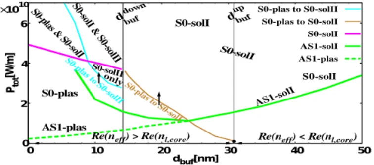
cal simulations providing both the dispersion curves and the associated field profiles like the ones shown above, we obtain the phase diagram of the improved NPSW for the main modes. Such diagram is shown in Fig.6where the existence and the type of the first symmetric and asymmetric modes are given. The buffer thickness dbu f and the total power Ptotare used as
parameters. The upper critical value dupbu f is 30.8 nm. Above this critical value, one has<e(ne f f) < <e(nl,core)and the nonlinear symmetric mode emerges from the cosine linear solution (see Fig.2(b)). It is of S0-solI type (symmetric soliton-type with a sin-gle peak, see solid profile in Fig.4(a)). For the critical value dupbu f, the black circle in Fig.6corresponds to the limit case where the Hyfield profile is still flat (see Fig.5(b) for an example of such
profile), for higher powers a core peak emerges. For d<dupbu f, one has<e(ne f f) > <e(nl,core)and the first symmetric mode of
the NPSW is of plasmonic type (see dashed curve in Fig.4(d)). Below this critical value for dbu f, and under the brown transition
curve in Fig.6, one has the S0-plas region, and above this curve the first symmetric mode is now of S0-solI type (see solid pro-file in Fig.4(d)). Along the brown curve in the phase diagram, the Hy field profile is flat. From ddownbu f = 14.5 nm, the lower
critical dbu f value, a new type of symmetric nonlinear solution
emerges, at high powers, from the S0-plas mode; it is composed of two solitons located in the core near each interfaces (see its symmetric field profile in inset in Fig.7). We denote it S0-solII. The transition curve between the S0-plas region and the S0-solII region is shown in cyan in the phase diagram. The limit curve above which the S0-solI mode appears is the pink one in Fig.6. It is worth mentioning that in the region above the cyan transition curve and below the pink limit curve, only the S0-solII mode exists. In Fig.6, we also provide the behaviour of the first asym-metric mode (green curves). The dashed green curve is the limit curve of the asymmetric plasmonic mode AS1-plas (see Fig.4(e)): below the curve, it does not exist. It emerges at low powers from the symmetric one, S0-plas (see Fig.4(d)). At higher powers (see the solid green line), it moves to an asymmetric mode of solitonic type AS1-solI (a peak is located in the core near one of its interface, see solid profile in Fig.4(e)). Above dbu f '24 nm,
only this AS1-solI mode exists and it emerges from the S0-solI symmetric mode as expected (see Figs.4(d) and (e)).
The permittivities being fixed, we numerically studied the in-fluence of the core thickness dcoreon the critical values ddownbu f ,
and dupbu f (see Fig. 5), we found that dupbu f does not change with dcorefor dcore ≥ 10 nm, while ddownbu f increases with dcore
(data not shown), such that they coincide when the core thick-ness reaches the critical value dλ
core ' 1550nm (one
wave-length), above this core thickness, the critical value ddownbu f will no longer change with dcore. Actually, it is possible to get an
analytical approximation for dupbu f considering a buffer layer sandwiched between semi-infinite metal and high-index di-electric regions, one gets, when|<e(εmet)| |εl,core|, dupbu f =
(λεbu f)/(2π|<e(εmet)|1/2(<e(εl,core) − <e(εbu f))) ' 28.4 nm.
This simple approximated value agrees well with the simu-lations results (30.8 nm) while the full formula (not shown) for dupbu f gives the better approximation 31.1 nm. Since at dupbu f, the mode is flat in the nonlinear core (see Fig.5(b)) as in the approx-imated model, it can be understood why both formula, that do not depend on dcore, provide a good approximation of dupbu f.
In Fig.7, we provide the phase diagram of the improved NPSW using dcoreand Ptotas parameters. The meaning of the curves are
the same as in Fig.6. We found that the threshold for the Hopf bifurcation, from which the asymmetric mode emerges, strongly decreases with the core thickness as it was already found in the simple NPSW [6,20]. One clearly sees that there is a critical value, denoted by dcritcorearound 430 nm for dbu f =15 nm such
that below it, only the S0-plas and the S0-solI modes exist (see Fig.4(d)). This low dcoreregion is split in two parts by the
transi-tion curve (brown one): below it, only the S0-plas exists while above only the S0-solI exists as fundamental symmetric mode. From dcritcorevalue up to the value dλcore'1550 nm, at some
pow-ers the S0-plas mode move to the S0-solII mode (cyan curve) and at even higher powers the S0-solI mode emerges (pink curve). For dcoreabove 1550 nm, the emergence of the S0-solI mode
ap-pears at powers lower than the transition between the S0-plas mode and the S0-solII one.
0 2 0 10 20 30 40 50 dbuf[nm] AS1-plas AS1-solI
Re(neff) < Re(nl,core) Re(neff) > Re(nl,core)
Fig. 6.Phase diagram of the improved NPSW as a function of dielectric buffer thickness dbu f and of the total power Ptotfor
dcore=400 nm and εbu f =2.52. The green curves refer to the
first asymmetric modes. Arrows indicate the corresponding mode transition across the associated curve (thin one).
The green AS1-plas and the AS1-solI dispersion curves (see mode profiles in Fig.4(e)) shown in Fig.7merge when they cross the brown curve associated with the transition from the S0-plas mode to the S0-solI one for increasing power. A similar phenomenom was already visible in Fig.6. After this merging, above the brown S0-plas/S0-solI transition curve, the AS1-plas mode does not exist anymore. In a previous work, using two
dif-1 2 3 ×10¹⁰ 500 1000 1500 2000 2500 3000 P[Wtot /m ] dcore[nm] S0-solI S0-plas to S0-solII S0-plas to S0-solI S0-solI AS1-solI AS1-plas S0-plas to S0-solI S0-plas to S0-solII S0-solII only
S0-solI & S0-solII
S0-plas & S0-solI
AS1-plas AS1-solI S0-solII mode profile dcore crit
Fig. 7.Phase diagram of the improved NPSW as a function of the nonlinear core thickness dcoreand of Ptot, for dbu f =15 nm
and εbu f =2.52. The green curves refer to the first asymmetric
mode. Inset: Hy(x)field profile for the S0-solII mode.
ferent numerical methods including the FDTD, we have already shown that the results about the stability of the main symmetric and asymmetric modes derived in reference [23] from theoretical arguments in the framework of the weak guidance approxima-tion in nonlinear waveguides are still valid, at least numerically, in simple NPSWs except just around the bifurcation point where subtle behaviours occur [20]. Here, we have again used the non-linear capabilities of the FDTD method implemented in theMEEP
software [24]. The metal permittivity is described by a Drude model to obtain the fixed negative value used at the studied wavelength in the stationnary study. As it can be seen in Fig.8, for the improved NPSW, the symmetric mode S0-solI is stable at low power. The S0-plas mode (plasmonic type) is also stable as expected from the results in [20] for the simple NPSW. The asymmetric mode AS1-solI is also stable for the tested powers above the bifurcation threshold (data not shown). Due to the losses of the metal, and as pointed out in [20,25], the temporal nonlinear solutions are actually not self-coherent [19] as it can be seen in Fig.8with the decrease of the field intensity along the propagation.
We have proposed an improved nonlinear plasmonic slot waveguide adding supplementary dielectric buffer layers
be-of the S0-solI symmetric solitonic type mode at a power such thath∆ni =0.043 for dcore=300nm, dbu f =40 nm, εbu f =2.52,
other parameters as in the text.h∆niis the spatial average along the core of the nonlinear refractive index change [6,20].
tween the nonlinear core and the metal regions. We have pro-vided a complete description of its main nonlinear TM modes. We have shown that this structure allows a decrease of the losses compared to the simple nonlinear slot waveguide, and that its main modes exhibit, for appropriate opto-geometric parameters, spatial transitions that can be controlled by the power. The stabil-ity of the main modes has also been demonstrated numerically.
REFERENCES
1. E. Feigenbaum and M. Orenstein, Opt. Lett.32, 674–676 (2007).
2. A. R. Davoyan, I. V. Shadrivov, and Y. S. Kivshar, Opt. Express16,
21209–21214 (2008).
3. A. R. Davoyan, I. V. Shadrivov, and Y. S. Kivshar, Opt. Express17,
21732–21737 (2009).
4. I. D. Rukhlenko, A. Pannipipitiya, M. Premaratne, and G. Agrawal, Phys. Rev. B84, 113409 (2011).
5. A. Ferrando, C. Milián, and D. V. Skryabin, J. Opt. Soc. Am. B30,
2507–2522 (2013).
6. W. Walasik, A. Rodriguez, and G. Renversez, Plasmonics10, 33–38
(2015).
7. J. R. Salgueiro and Y. S. Kivshar, Appl. Phys. Lett.97, 081196 (2010).
8. N. Nozhat and N. Granpayeh, Opt. Commun.285, 1555–1559 (2012).
9. Z. Han, A. Y. Elezzabi, and V. Van, Opt. Lett.35, 502–504 (2010).
10. G. I. Stegeman and C. T. Seaton and J. Ariyasu and R. F. Wallis and A. A. Maradudin, J. Appl. Phys.58, 2453–2459 (1985).
11. W. Walasik, V. Nazabal, M. Chauvet, Y. Kartashov, and G. Renversez, Opt. Lett.37, 4579–4581 (2012).
12. W. Walasik and G. Renversez, Phys. Rev. A93, 013825 (2016).
13. B. M. A. Rahman, J. R. Souza, and J. B. Davies, IEEE Photon. Technol. Lett.2, 265–267 (1990).
14. A. Ferrando, M. Zacarés, P. F. de Cordoba, D. Binosi, and J. A. Monso-riu, Optics Express11, 452–459 (2003).
15. F. Drouart, G. Renversez, A. Nicolet, and C. Geuzaine, J. Opt. A: Pure Appl. Opt.10, 125101 (2008).
16. W. Walasik, G. Renversez, and Y. V. Kartashov, Phys. Rev. A89,
023816 (2014).
17. F. Zolla, G. Renversez, A. Nicolet, B. Kuhlmey, S. Guenneau, D. Fel-bacq, A. Argyros, and S. Leon-Saval, Foundations of Photonic Crystal Fibres (Imperial College Press, London, 2012), 2nd ed.
18. A. W. Snyder and J. D. Love, Optical Waveguide Theory (Chapman and Hall, London, 1983).
19. A. W. Snyder, D. J. Mitchell, and L. Poladian, J. Opt. Soc. Am. B8,
1618–1620 (1991).
20. W. Walasik, G. Renversez, and F. Ye, Phys. Rev. A93, 013826 (2016).
21. K. Y. Bliokh, Y. P. Bliokh, and A. Ferrando, Phys. Rev. A79, 041803
(2009).
22. C. Miliàn, D. E. Ceballos-Herrera, D. V. Skryabin, and A. Ferrando, Opt. Lett.37, 4221–4223 (2012).
23. D. J. Mitchell and A. W. Snyder, J. Opt. Soc. Am. B10, 1572–1580
(1993).
24. A. F. Oskooi, D. Roundy, M. Ibanescu, P. Bermel, J. D. Joannopoulos, and S. G. Johnson, Comput. Phys. Commun.181, 687–702 (2010).
REFERENCES
1. E. Feigenbaum and M. Orenstein, “Plasmon-soliton,” Opt. Lett.32,
674–676 (2007).
2. A. R. Davoyan, I. V. Shadrivov, and Y. S. Kivshar, “Nonlinear plasmonic slot waveguide,” Opt. Express16, 21209–21214 (2008).
3. A. R. Davoyan, I. V. Shadrivov, and Y. S. Kivshar, “Self-focusing and spatial plasmon-polariton solitons,” Opt. Express17, 21732–21737
(2009).
4. I. D. Rukhlenko, A. Pannipipitiya, M. Premaratne, and G. Agrawal, “Exact dispersion relation for nonlinear plasmonic waveguides,” Phys.
Rev. B84, 113409 (2011).
5. A. Ferrando, C. Milián, and D. V. Skryabin, “Variational theory of soli-plasmon resonances,” J. Opt. Soc. Am. B30, 2507–2522 (2013).
6. W. Walasik, A. Rodriguez, and G. Renversez, “Symmetric plasmonic slot waveguides with a nonlinear dielectric core: Bifurcations, size effects, and higher order modes,” Plasmonics10, 33–38 (2015).
7. J. R. Salgueiro and Y. S. Kivshar, Nonlinear plasmonic directional couplers, Appl. Phys. Lett.97, 081196 (2010).
8. N. Nozhat and N. Granpayeh, “Switching power reduction in the ultra-compact Kerr nonlinear plasmonic directional coupler,” Opt. Commun.
285, 1555–1559 (2012).
9. Z. Han, A. Y. Elezzabi, and V. Van, “Experimental realization of sub-wavelength plasmonic slot waveguides on a silicon platform,” Opt. Lett.
35, 502–504 (2010).
10. G. I. Stegeman and C. T. Seaton and J. Ariyasu and R. F. Wallis and A. A. Maradudin, J. Appl. Phys.58, 2453–2459 (1985).
11. W. Walasik, V. Nazabal, M. Chauvet, Y. Kartashov, and G. Renversez, “Low-power plasmon–soliton in realistic nonlinear planar structures,”
Opt. Lett.37, 4579–4581 (2012).
12. W. Walasik and G. Renversez, “Plasmon-soliton waves in planar slot waveguides. I. modeling,” Phys. Rev. A93, 013825 (2016).
13. B. M. A. Rahman, J. R. Souza, and J. B. Davies, “Numerical analysis of nonlinear bistable optical waveguides,” IEEE Photon. Technol. Lett.
2, 265–267 (1990).
14. A. Ferrando, M. Zacarés, P. F. de Cordoba, D. Binosi, and J. A. Monso-riu, “Spatial soliton formation in photonic crystal fibers,” Optics Express
11, 452–459 (2003).
15. F. Drouart, G. Renversez, A. Nicolet, and C. Geuzaine, “Spatial Kerr solitons in optical fibres of finite size cross section: beyond the Townes soliton,” J. Opt. A: Pure Appl. Opt.10, 125101 (2008).
16. W. Walasik, G. Renversez, and Y. V. Kartashov, “Stationary plasmon-soliton waves in metal-dielectric nonlinear planar structures: modeling and properties,” Phys. Rev. A89, 023816 (2014).
17. F. Zolla, G. Renversez, A. Nicolet, B. Kuhlmey, S. Guenneau, D. Fel-bacq, A. Argyros, and S. Leon-Saval, Foundations of Photonic Crystal Fibres (Imperial College Press, London, 2012), 2nd ed.
18. A. W. Snyder and J. D. Love, Optical Waveguide Theory (Chapman and Hall, London, 1983).
19. A. W. Snyder, D. J. Mitchell, and L. Poladian, “Linear approach for approximating spatial solitons and nonlinear guided modes,” J. Opt. Soc. Am. B8, 1618–1620 (1991).
20. W. Walasik, G. Renversez, and F. Ye, “Plasmon-soliton waves in planar slot waveguides. II. results for stationary waves and stability analysis,” Phys. Rev. A93, 013826 (2016).
21. K. Y. Bliokh, Y. P. Bliokh, and A. Ferrando, “Resonant plasmon-soliton interaction,” Phys. Rev. A79, 041803 (2009).
22. C. Miliàn, D. E. Ceballos-Herrera, D. V. Skryabin, and A. Ferrando, “Soliton-plasmon resonances as Maxwell nonlinear bound states,” Opt.
Lett.37, 4221–4223 (2012).
23. D. J. Mitchell and A. W. Snyder, “Stability of fundamental nonlinear guided waves,” J. Opt. Soc. Am. B10, 1572–1580 (1993).
24. A. F. Oskooi, D. Roundy, M. Ibanescu, P. Bermel, J. D. Joannopoulos, and S. G. Johnson, “MEEP: A flexible free-software package for electro-magnetic simulations by the FDTD method,” Comput. Phys. Commun.
181, 687–702 (2010).
25. J. R. Salgueiro and Y. S. Kivshar, “Complex modes in plasmonic non-linear slot waveguides,” J. of Optics16, 114007 (2014).