Characterization of Anodic Bonding
By
Carissa Debra Tudryn
B.M.E. Bachelor of Mechanical Engineering The Catholic University of America, 2000
SUBMITIED TO THE DEPARTMENTS OF MECHANICAL ENGINEERING AND MATERIALS SCIENCE AND ENGINEERING IN PARTIAL FULFILLMENT OF
THE REQUIREMENTS FOR THE DEGREES OF MASTER OF SCIENCE IN MECHANICAL ENGINEERING
MASTER OF SCIENCE IN MATERIALS SCIENCE AND ENGINEERING AT THE
MASSACHUSETIS INSTITUTE OF TECHNOLOGY FEBRUARY 2004
© 2004 Carissa Debra Tudryn. All rights reserved.
The author hereby grants to MIT permission to reproduce and to distribute publicly paper and electronic copies of this thesis docurT]ent in whole or in part.
Si nature of author /. ~'-' \.' V • ' - . / ? ' '---' ~ _ ~ ~
Departments of Mec anical Engineering and Materials Science a; Engineering
/ ) 1 I February 2004
Certified by
Certified by
/
/
Ralph HopkinsCharles Stark Draper Laboratory Thesis Supervisor
{/ S. Mark Spearing
Associate/Professor of Aeronautics and Astronautics
- Thesis Advisor
Certified by
Linn Hobbs
Professor of Material~ce and Engin~ a~d Nuclear Engineering
"'- Thesis Advisor Certified by Accepted by MASSACHUSETTS INS E. OF TECHNOLOGY
JUL 2 0
2IJOIt
I
David Parks ~.61 of Mechanical Engineering Thesis Reader ~ Ain A. SoninChairman, Committee on Graduate Studies Department of Mechanical Engineering
Characterization of Anodic Bonding
ByCarissa Debra Tudryn
Submitted to the Departments of Mechanical Engineering and Materials Science and Engineering on January 16, 2003, in partial fulfillment of the requirements for the dual degrees of Master of Science in Mechanical Engineering and Master of Science in
Materials Science and Engineering.
Abstract
Anodic bonding is a common process used in MicroElectroMechanical Systems (MEMS) device fabrication and packaging. Polycrystalline chemical vapor deposited (CVD) silicon carbide (SiC) is emerging as a new MEMS device and packaging material because of its excellent material properties including high strength, hardness, and thermal conductivity. An alternative, low temperature glass to CVD SiC anodic bonding process is required in order to prevent gold tin braze stress relaxation. A novel process recipe, requiring a SiC
RMS surface roughness of 45nm, was developed for anodically bonding CVD SiC to bulk and thin-film, lapped PyrexTM and Hoya SD-2TM glass substrates. The bond quality,
residual curvature, and microstructured interfacial features for CVD SiC anodic bonding were shown to be comparable to single crystal silicon (Si) anodic bonding. The Plaza Test specimen, invented by Plaza et al., was used to assess bulk and thin-film, lapped
glass bond quality. A two-part contact/bonding model was used to predict the contact and bonding of the Plaza Test structures. Surface contact was predicted by a parallel plate capacitor pull-in model after the voltage was applied, and linear elastic fracture mechanics (FEA) modeling predicted the toughness or work-of-adhesion of the bonded surfaces after the formation of a permanent silicon dioxide bond. The role of the voltage, structure geometry, work of adhesion, and materials used in the model predicted that the bonding mechanism limited the total number of structures that remained bonded. The thin-film, lapped glass bond quality improved when increasing the voltage and time. The calculated, experimental, and modeled thermoelastic curvatures were minimal, indicating low residual stress between the bonded materials. Finally, microscopy and elemental analysis showed distinct differences in elemental depletion band(s) of bulk PyrexTM and Hoya SD-2TM glasses bonded to Si, and in interfacial bonding between PyrexTM and CVD SiC compared to PyrexT M and Si. More elements in the glass network are identified as
participating in the depletion layer process than identified in previous studies. Overall, the process recipes, modeling, experimental work, and chemical analysis of glass to
CVD SiC anodic bonding showed that CVD SiC can be bonded successfully and be a
promising packaging material.
Thesis Supervisor: Ralph Hopkins
Title: Staff, Charles Stark Draper Laboratory Thesis Advisor: S. Mark Spearing
Title: Associate Professor of Aeronautics and Astronautics Thesis Advisor: Linn Hobbs
Title: Professor of Materials Science and Engineering and Nuclear Engineering Thesis Reader: D. Parks
Acknowledgements
I would like to express my sincere gratitude to the following people for their
guidance, wisdom, and assistance in my dual masters thesis. This thesis
involved an extensive amount of thought, fabrication work, and experimental and modeling analysis, which could not have been done by myself. I am also grateful to have been offered a Draper Fellowship. I received the best of both worlds, MIT and Draper, and the best of two masters in Mechanical Engineering and Materials Science and Engineering.
I truly appreciated the lengthy insight, edifying discussions, constant supervision,
and challenges from my primary MIT advisors, Profs. Mark Spearing and Linn Hobbs. I'm very grateful to my MIT reader, Prof. David Parks, who gave me insight into future modeling analysis. By attending Spearing's group meetings, I gained a lot of knowledge from other graduate student's research, and their suggestions and observations were valuable to my own research. I thank Kevin Turner for all the discussions, patience, and wisdom. I also express thanks to Hyung-Soo Moon, Dongwon Choi, Christine Tsau, DJ Shim, and Jeremy Gregory. I'm appreciative to Ivan Lee, and Rob Bernstein for use of their lab equipment. I'm grateful to Dr. Stefan Schweizer who assisted me with the
arduous TEM prep and analysis. A big thanks to Leslie Regan who always lends a helping hand and ear to each graduate student.
I truly appreciated my Draper Supervisor's, Ralph Hopkins, constant availability,
knowledge, patience, and confidence in my research. A sincere thank you to all the Draper technicians and staff who were always catering to my frequent needs involving fabrication work, equipment/software use, or research discussions: Jeff Borenstein, Amy Duwel, Bill Sawyer, Mark Mescher, Matt Varghese, Dave
Nokes, Connie Cardoso (my saving grace), Manuela Healy, Bessy Silva, Katherine Ashton, Isaac Costa, Brian Orrick, Mert Prince, Jim Cousens, Bill Donovan, Dave Porter, Peter Sebelius, Richard Caruso, and Jim Bickford. Thank you to the staff who gave me a gift of a Draper window office during my final months.
Not only did I bond samples, but I also had the pleasure of bonding with my friends, roommates, and off icemates in order to escape the stresses of class and
research: Sarah, Yabei, Marisa, Cari, Robin, Janelle, Femme Cards, PERG, Chris, Anne, Aimee, Kevin, Jaime, Nadine, Mimi, Krissa, Matt, Jeb, Kara,
Kyrilian, Gary, Raj, and Dave. I also met many friends along the way training with the MIT Triathlon Club and for marathons, being on AHEC, and involved with NMB and Mars Society. I thank COL Young for all his support and funding of the JPL Mars Mission Robotics Videoconferences. Every evening I came back to a pleasant dorm, Ashdown: thank you, Terry and Anne, Denise, and Cissy.
I have been blessed with a family, who has been a perpetual support throughout
Daddeo), brother (T J), and sister's (Jessica and Melissa) undying faith, sacrifice, soothing spirit, guidance, judgment, and love have built the person I am today. My grandparents (Nana, Papa, Omi, and Opa), aunts, uncles, and cousins have also given me undying love, support, and encouragement. Each has allowed me to keep my "out-of-this-world" dream alive.
Last, but not least, thank you, Alexis. You have a special place in my heart, and I look forward to learning and dreaming with you.
"Commit to the Lord all you can and your plans will succeed. II Proverb 16:3
MARS OR BUST ...
This thesis was prepared by The Charles Stark Draper Laboratory, Inc., under Internal Company Sponsored Research Project C301, SOA - System
Engineering/Program Management.
Publication of this thesis does not constitute approval by Draper of the findings or conclusions contained herein. It is published for the exchange and stimulation of
ideas. , r , • / ' - \ J "1
Table of Contents
Chapter 1 Introduction ... 13
1.1 Device Packaging... 13
1.2 Device-Attachm ent Process Requirements... 14
1.3 Review of Underpinning Technologies... 15
1.3.1 Anodic Bonding... 15
1.3.2 SiC for M EMS... 15
1.3.3 Packaging... 16
1.4 Research O bjectives ... 16
1.5 Thesis O utline ... 16
Chapter 2 Review of Science and Technology of Anodic Bonding ... 19
2.1 Anodic Bonding Bulk G lass to Silicon ... 19
2.1.1 Mechanism s... 19
2.1.2 Strength and Toughness Methods to Characterize Anodic Bond Q uality... 28
2.1.3 Bond Q uality using the Test Specimen: Plaza Test Mask... 29
2.2 Thin-Film G lass to Silicon Anodic Bonding ... 32
2.3 SiC Anodic Bonding ... 36
2.4 Device-Attachm ent Process Developm ent... 37
Chapter 3 Modeling of Bulk Glass to Silicon and CVD Silicon Carbide... 39
3.1 Materials Modeled ... 39
3.2 Plaza Test Mask Deform ation Model ... 41
3.3 Two-Part Bond Model... 44
3.3.1 Contact: Parallel Plate Capacitor Pull-in Model ... 46
3.3.2 Bonding: Linear Elastic Fracture Mechanics (LEFM) Modeling... 55
3.3.3 Flow Diagram of Contact and Bonding... 65
3.4 Curvature Calculations ... 68
3.4.1 Classical Plate Theory ... 69
3.4.2 Curvature Calculation from Classical Plate Theory... 71
3.4.3 Curvature Calculation from Experimental Results ... 78
3.4.4 ANSYSv.6.0 Curvature Modeling ... 80
Chapter 4 Anodic Bonding of Bulk Glass to Silicon and CVD Silicon Carbide ... 83
4.1 Experim ental Procedure ... 83
4.1.1 Process Variables... 85
4.1.2 Anodic Bonding Equipm ent... 86
4.1.3 Contact Angle Measurement... 87
4.1.4 Anodic Bonding using CVD SiC ... 88
4.1.5 TEM and STEM/XEDS W ork... 88
4.2 Results and Discussion ... 89
4.2.1 Hydrophilic versus Hydrophobic Surfaces... 89
4.2.2 JM Pv.3.1 Experim ental Matrix Results... 94
4.2.3 Two-Part Bond Model Results... 96
4.2.4 Curvature Values ... 105
4.2.5 TEM and STEM/XEDS Chem ical Results... 108
Chapter 5 Anodic Bonding of Thin-Film Glass to Silicon and CVD Silicon Carbide...119
5.1 Experim ental Procedure ... 119
5.1.1 Sputtered PyrexTm Glass Procedure... 119
5.1.2 Lapped Glass Procedure ... 121
5.2 Results and Discussion ... 123
Chapter 6 Conclusions and Recom mendations for Future W ork...139
6.1 Conclusions... 139
6.2 Recom mendations for Future W ork... 140
Chapter 7 Appendix...143
List of Figures
Figure 1-1: SiC Packaging of a MEMS Device ... 13
Figure 2-1: Processes Occurring at the Interface During Anodic Bonding ... 20
Figure 2-2: Current vs. Time: PyrexTM bonded to Si at 1kV, 350"C, 10 m inutes... 21
Figure 2-3: Albaug h's Model [12] ... 22
Figure 2-4: Glass Network [6] ... 24
Figure 2-5: Hydrophilic Surface Bonds [21]... 27
Figure 2-6: Plaza Die Test Mask... 30
Figure 2-7: Plaza Test Structures [26]... 30
Figure 2-8: Plaza Test Mask Bonded Sample ... 31
Figure 2-9: Thin-Film Anodic Bonding Process ... 33
Figure 2-10: XPS Analysis Sodium [25] ... 34
Figure 2-11: XPS Analysis of Oxygen and Silicon [25]... 35
Figure 3-1: Effective Delta TCE of Glass to Si and CVD SiC as a function of temperature. (TCEgas - TCEsu/sic) [28]. 41 Figure 3-2: Schematic of the Pre-Anodic Bond of Die Size Sam ple... 42
Figure 3-3: Schematic of the Post- Anodic Bond of Die Size Sample ... 42
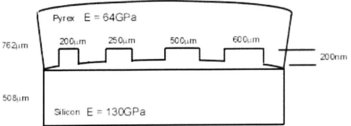
Figure 3-4: Side View of Structure Modeled... 43
Figure 3-5: Top View of Plaza Test Mask Array in Glass... 44
Figure 3-6: Force Diagram ... 45
Figure 3-7: Surface Contact... 45
Figure 3-8: Surface Bonding ... 46
Figure 3-9: Spring-Mass Structures of Parallel Plate [1] and Plaza Test structure... 47
Figure 3-10: Dimensions of Bonded Structure... 48
Figure 3-11: PyrexTM Glass Deformation ... 49
Figure 3-12: Silicon Deformation... 49
Figure 3-13: Parallel Plate Capacitor [1] versus Anodic Bond Sample... 50
Figure 3-14: Sodium depletion layer thickness in Tempax as a function of the drift time at various temperatures and drift voltage of 250V [6]... 51
Figure 3-15: Two-port Voltage Controlled Capacitor [1]... 53
Figure 3-16: Voltage Controlled Electrostatic Actuator [1] ... 53
Figure 3-17: Sym metric Front of Structure ... 56
Figure 3-18: Crack Closing Dimensions... 57
Figure 3-19: Sym metric ANSYS Model of Structure ... 58
Figure 3-20: Two Deformed Interface Nodes (Not drawn to Scale) ... 59
Figure 3-21: G versus Crack Length for 600pim Structure ... 62
Figure 3-22: G as a Function of W ... 62
Figure 3-23: Acoustic Microscopy Image of Crack Length and Total Area Modeled ... 63
Figure 3-24: Bonded Structures and their Corresponding Minim um G... 64
Figure 3-25: Contact and Bond Model Flow Chart... 67
Figure 3-26: Bilayer Geometry [34]... 70
Figure 3-27: Plate Curvature [35]... 70
Figure 3-28: Die Size Sample Scan ... 78
Figure 3-29: Bow Calculation ... 79
Figure 3-30: Bow Geometry ... 80
Figure 3-31: ANSYSv6.0 3-D Bimaterial Dimensions with Boundary Conditions ... 81
Figure 3-32: Side View of the deflection of PyrexTM glass bonded to silicon at AT=-330'C...82
Figure 4-1: Schematic of the Anodic Bonder... 87
Figure 4-2: Contact Angle ... 88
Figure 4-3: Bonded Sample with Hydrophobic Si Surface ... 92
Figure 4-4: Bonded Sample with Hydrophilic Si Surface ... 93
Figure 4-5: Hydrophilic vs. Hydrophobic P-type Si to Glass Bonding Current ... 94
Figure 4-6: Acoustic Microscope Image of Bonded vs. Unbonded structures of Exp.1 Part 1 ... 97
Figure 4-7: DEKTAK 3STv.2.12 Surface Scan of Pyrex/Si Bonded Structures... 98
Figure 4-8: PyrexTM /Silicon Deformation of 600 Iam W idth Structure... 98
Figure 4-9: Fe as a function of W vs. Fk for PyrexTM and Si (1 kV, go = 0.2ptm etch depth) ... 99
Figure 4-10: F, as a function of etch depth (go) vs. Fk of PyrexTM and Si at 1 kV... 101
Figure 4-11: Delta K of PyrexTM/Si as a function of Temperature... 106
Figure 4-12: Delta K of Hoya SD-2TM/Si as a function of Temperature... 107
Figure 4-13: Curvature Values from Experiments 1 and 2... 108
Figure 4-14: TEM Picture of PyrexTM /Si Layer ... ... ... 109
Figure 4-15: TEM Picture of Hoya SD-2TM /Si Layers ... 110
Figure 4-16: TEM Image of PyrexTM/CVD SiC Interfacial Features... 111
Figure 4-18: Current - time Profiles for PyrexTM bonded to Si and CVD SiC ... 113
Figure 4-19: Ratio of Key Elements of Hoya SD-2TMto Silicon ... 115
Figure 4-20: Ratio of Key Elements of PyrexTM Glass to Silicon Part 1 ... 116
Figure 4-21: Ratio of Key Elements of PyrexTM Glass to Silicon Part 2... 117
Figure 5-1: Anodic Bonding of Sputtered Pyr TM Glass to Silicon... 121
Figure 5-2: Anodic Bonding of Lapped Glass to Silicon... 122
Figure 5-3: Difference of Bonding Bulk Glass to Lapped Glass using Reverse Polarity... 124
Figure 5-4: Side View of Lapped Sample ... 126
Figure 5-5: Image of First PyrexTM-Si Bulk Anodic Bond... 127
Figure 5-6: W aveform of 1st Full W afer Anodic Bond of Si-PyrexTM of Sample 1 ... 129
Figure 5-7: Image of Die Size Anodic Bond of Sample #1 ... 131
Figure 5-8: Sample #2 Die Size Bond at 3500C, 80V, and 20 min... 133
Figure 5-9: Sample of Si-Lapped PyrexTM to CVD SiC Bonded at 3500C, 80V, and 45 min... 134
List of Tables
Table 1: PyrexTM and Hoya SD-2TM Glass Composition... 23
Table 2: Modulus of Elasticity and Poisson's Ratio of Materials [26]" ... 40
Table 3: Shear Modulus of Materials [27] ... 40
Table 4: Minim um Strain Energies as a Function of Deformation ... 60
Table 5: Final Calculation of G, Energy Release Rate... 61
Table 6: Material Tem perature Properties [33] "... 69
Table 7: Silicon Stiffness Material Constants [37]... 73
Table 8: Elastic Constants as a Function of Tem perature [37] ... 73
Table 9: Average Biaxial Modulus... 74
Table 10: Effective Alpha for PyrexTM...76
Table 11: Effective Alpha for Hoya SD-2TM...76
Table 12: Effective Alpha for Silicon [26]... 76
Table 13: Effective Alpha for CVD SiC ... 77
Table 14: Thickness Error Bars ... 77
Table 15: AT Error Bars ... 77
Table 16: Total Sources of Error ... 78
Table 17: JMPv.3.1 Experimental Matrix... 86
Table 18: TEM/STEM Bonding Matrix ... 89
Table 19: Contact Angles of Materials... 91
Table 20: Results of JM Pv.3.1 Experim ental Matrix: Exp. 1 Glass to Silicon ... 95
Table 21: Results of JM Pv.3.1 Experimental Matrix: Exp. 2 Glass to Silicon Carbide... 96
Table 22: Deformation of 600ptm Structures with 0.2pm Etch Depth ... 98
Table 23: Table of V, Predicting Contact at Minim um W t versus Minim um W t Bonded ... 100
Table 24: Minim um G Results of Experiments 1 and 2... 103
Table 25: Final Modeling Results of Experiments 1 and 2... 104
Table 26: Measured PyrexTM Com position by XPS [41]... 114
Table 27: Measured Hoya SD-2TM Com position ... ... ... ... 114
Chapter 1 Introduction
1.1 Device Packaging
Device packaging design is critical to the performance of MEMS
(MicroElectroMechanical Systems) microsensor and microactuator devices. The device package provides a stable thermal and mechanical environment, and electrical and hermetic isolation from the external environment [1,2]. A crucial step in the fabrication of a MEMS device is the method used to attach it to the package. The device-attachment method must provide high stability, low creep, low residual stress, and reliable process control.
The system under study is shown in Figure 1-1. The silicon-on-glass MEMS sensor device is attached to a polycrystalline, chemical vapor deposited (CVD) silicon carbide (SiC) package. Typically, a gold-tin braze is used to attach the
MEMS device to the CVD SiC packaging. The gold-tin braze yield point is
exceeded during the device-attachment, (packaging process), causing creep and/or stress relaxation over time. An alternative device-attachment process is needed to reduce and/or eliminate this gold-tin braze stress relaxation.
Cap
W..Gold-Tin Braze
Figure 1-1: SiC Packaging of a MEMS Device
1.2 Device-Attachment Process Requirements
A low-temperature device-attachment process is desirable to implement
high-strength, stable bonds between the MEMS device and its package. Anodic bonding is a preferred bonding technique, because it is a low temperature process and produces hermetic and mechanically strong seals [3]. A low temperature packaging process is advantageous because it avoids potential degradation of and damage to the MEMS device and circuitry, and minimizes residual stresses generated by the thermal expansion coefficient (TCE)
difference between the materials [3]. Large residual stresses negatively affect the performance of the MEMS device. These stresses lead to distortions in the device output, and in extreme circumstances may cause bond failure.
CVD SiC is emerging as a MEMS packaging material because of its excellent
material properties and close TCE match to common materials such as silicon (Si), and HOYA SD-2TM and Pyrex TM (Corning #7740) glasses. Other desirable
SiC properties include high strength, chemical resistance, thermal conductivity, hardness, and hermeticity, which are all important for use in harsh environments and in high temperature, power, and frequency devices [4]. Pyrex TM is a
borosilicate glass that has been the most widely used to bond to Si because of its high sodium content (known to be a significant factor in the anodic bonding
mechanism) and the fact that it has a close TCE to Si. More recently, Hoya
SD-2TM glass has been formulated for Si anodic bonding applications because its
TCE is more closely matched to Si, from room temperature to the bonding temperature than PyrexT M [5]. HOYA
SD-2TM and Pyrex TM are closely matched
in TCE to Si and to CVD SiC over a wide temperature range, as shown in Section 3.1.
The overall approach of using CVD SiC anodic bonding to glass as a packaging solution will benefit the MEMS field significantly. A low stress packaging
process, using the anodic bonding technique and CVD SiC, PyrexTM , and Hoya
such as RF devices, gyroscopes and accelerometers, and precision optical devices.
1.3 Review of Underpinning Technologies
1.3.1 Anodic Bonding
Anodic bonding involves the bonding of glass or ceramics to Si or metals under an applied voltage (200-1 000V) and elevated temperature (200-500C) [2]. This technique has been widely used in the MEMS field to bond a variety of glasses,
metals, alloys, and semiconductor materials [2]. Not only have Hoya SD-2TM and
Pyrex T M glasses been bonded to Si, but several other glasses have also been
bonded, such as the borosilicate glass, Corning #7070, Tempax (Schott #8330), soda lime # 0080, potash soda lead #0120, and aluminosilicate #1720 [2,6]. Several metals, alloys, and semiconductors with similar TCE have been bonded to these glasses, including, tantalum, titanium, Kovar, Niromet 44, Aluminum,
Fe-Ni-Co alloys, silicon, and gallium arsenide [2].
Bulk glass anodic bonding to Si is a mature technology, but bonding Si to Si using a thin glass film (thin film anodic bonding) is a less developed process. The development of a thin film anodic bonding process will enable fabrication of
MEMS devices having negligible residual stress [7]. Section 2.2 describes
Si-to-Si anodic bonding or thin-film glass anodic bonding processes in detail.
1.3.2 SiC for MEMS
SiC technology used in the MEMS field is still under development. There are a few examples of using SiC in fabrication processes. Micromachined
polycrystalline SiC micromotors have been fabricated using a multilayer fabrication process. This process uses low temperature deposition and
micromolding techniques to fabricate SiC structural components [8]. Presently,
SOI, silicon-on-insulator technology, is widely used in MEMS fabrication.
SiC-on-insulator or semi-insulating wafers are also used in microwave applications [4]. The "smart cut proceSSTMn is one technique being used to form SiC-on-insulator
[4] . Several other techniques have been explored, but all have several drawbacks such as defects produced from lattice mismatch, when growing epitaxially SiC on Si, and SiC surface roughness hindering direct bonding [9]. Tong et al. [9] explored an alternative process to develop SiC-on-insulator by using anodic bonding. Section 2.3 explains this process in detail.
1.3.3 Packaging
The technology of MEMS packaging continues to be an engineering intensive effort because almost every device requires a custom package development. The evolution of standard packaging methodologies that can be used for a wide variety of devices and applications will have a profound effect on the use of
MEMS in systems, for reasons of both improved functionality and reduced
development and production costs.
1.4 Research Objectives
There are three principal objectives of the research carried out for this thesis:
1. To establish a protocol in order to bond bulk and thin film PyrexTM and HOYA SD-2TM glass to CVD SiC.
2. To assess bond quality using the Plaza Test Mask [10].
3. To establish whether residual stresses formed after anodic bonding are
consistent with the expected thermoelastic response.
1.5 Thesis Outline
Chapter 2 begins with a review of the anodic bonding literature. This review presents a summary of the bulk glass anodic bonding mechanism, thin-film (Si-to-Si) and SiC anodic bonding techniques, and methods used to characterize anodic bond strength and toughness. There is also a discussion about the Plaza test specimen that is implemented in this study. Finally, Section 2.4 details the
device-attachment approach, deduced from available literature. Chapter 3 discusses modeling the bonding and bond toughness for bulk glass bonded to Si
and CVD SiC. Chapter 4 details experimental procedure, sample preparation, and process variables, for bonding bulk glass to Si and CVD SiC. This chapter also presents the results and a discussion of the modeling procedures described in Chapter 3, as well as the chemical analysis performed on bulk glass samples. In Chapter 5, two thin-film bonding techniques are discussed and their resulting bond quality assessed. Finally, Chapter 6 provides an overall conclusion and recommendations for future work.
Chapter 2
Review of Science and Technology of Anodic Bonding
2.1 Anodic Bonding Bulk Glass to Silicon
2.1.1 Mechanisms
Since the invention of anodic bonding in 1969 [11], there has been much research conducted to deduce the mechanisms involved. The following review describes the likely physical mechanisms, particularly as evidenced in current changes with time, and the supporting analytical chemical findings of several researchers.
Anodic bonding is performed by heating a glass and metal (or semiconductor) sandwich, across which a d. c. voltage is applied. Typically, a glass and p-type Si are bonded together. The cathode is attached to the glass and the anode to the Si, so that the Si is at a positive potential with respect to the glass. Figure 2-1 shows a schematic depiction of this electrochemical process [12]. Both silicon and glass remain relatively stiff during the bonding process, since temperatures well below the respective melting point of Si and glass transition temperature are used [12]. This irreversible bonding process produces a
permanent chemical bond at the glass/Si interface involving an intermediary Si0 2
interface layer [3,5,13]. With the application of heat and voltage, two types of reactions occur in forming this Si0 2 intermediate bond: ion dissociation/
association reactions and interfacial bonding reactions [14]. The elevated temperature permits ionic conduction within the glass, while the imposed
potential drives the migrating ions of opposite charge towards the interface or towards the cathode. The glass behaves as an electrolyte at elevated
temperatures because of these mobile ion species. Cations (principally Na) move through the glass toward the negatively-charged cathode. Since the cations move toward the cathode, a depletion layer is formed, and the glass
anionic oxygen species, under the influence of the electrostatic potential, to move towards the interface. The space charging of the depletion layer generates an interfacial electrostatic field. These electrostatic forces pull the glass and Si surfaces together, and hold them during the formation of a permanent bond. The contact starts at a single point between the interfaces, spreads over the
remaining area, and allows the diffusion of oxygen anions into the positively charged Si [13,15]. Bond formation can occur only between surfaces that are clean and have sufficiently low surface roughness. The surfaces must be clean because particles will cause unbonded regions and not allow for complete,
physical surface contact. Ko et al. [2] state that the glass and metal RMS surface roughness should be less than 1 lpm in order for bonding to occur.
Bulk Glass Na4 depletion Na4* Na4 Na* layer 0'--2To2- 0interface Silicon hot plate (C) Glass Na+ Na4* Na4 02 O02 - 2 -019 SiSi StSi Si Si 2. Movement of ions
near interface
1.
surface contact
and depletion layer
formation
Glass ilterfac 02 -i 0- Si Sificon-3. Oxygen anions
diffuse into silicon
network to form Si)
2Figure 2-1: Processes Occurring at the Interface During Anodic Bonding V
The progress of anodic bonding process is monitored typically via the current flowing through the circuit. Albaugh [12,16] modeled the current transient
response, d21/dt2, of the current (1) vs. time (t) plot in Figure 2-2. Figure 2-3
shows the depletion layer defined as a variable capacitor, and the bulk glass as a variable series resistor. The model was successfully fitted to the initial
experimental current transient response at short bonding times. Modeling longer bonding times proved less successful. This was presumed to be because of leakage across the depletion layer, and because there are several mobile ion species responsible for current flow [16]. Albaugh [12] determined that the
current decreases quickly at the beginning of the bonding process because of the initial charging of the depletion layer, and the area under this initial peak gives information about the amount of charge that is leaving the depletion layer.
E 1.20 - 1.05-0.90 -0.75 -0.60 -0.45 -0.30 -0.15 -0.00' 0 100 200 300 time(s) 400 500 600
Glass:
R
Depletion
7
Laye
r: C
Figure 2-3: Albaugh's Model [12]
The current vs. time kinetics are controlled by the imposed bonding conditions, such as voltage, temperature, environment, and surface chemistry, and Si
doping. The findings of Cozma and Puers [17] indicate that a larger in integrated current produces a higher bond quality, and faster overall bonding. Higher
voltage, and lower temperature increased the current peak, hence smaller bonding times were needed [17]. Longer times were needed when using low voltages, temperatures, and n-type silicon. The low voltages cause the electric field at the interface to be lower, so that the oxygen anions cannot drift with a high enough drift velocity and to maintain the high oxidation rate at the bond front. Lower temperatures do not allow the rapid build-up of space charge at the interface because of a glass conductivity that decreases exponentially with lower temperature [17]. Lee et al. [18] discovered that a longer time, in excess of 38 minutes, was needed when bonding n-type Si to PyrexTM glass, compared to the 4 minutes needed to bond p-type Si. Since p-type Si is doped (usually) with boron, it has extra holes in the Si valence band. Therefore, under a strong electric field, these can migrate toward the cathode (to the Si surface nearest the glass). Lee et al. maintain that there is a higher interfacial electrostatic pressure, which in turn, increases the bonding speed [18]. The bonding environment also affects the current peak. The current peak increased when bonding in air
compared to in vacuum or an argon environment [17]. However, the
mechanisms are unclear. Oxygen in air possibly participates in the bonding process, or the heat transfer in a vacuum is poor [17]. Finally, Cozma and Puers
[18] found that hydrophilic Si surfaces, resulting from treatment with a 65%
did not exhibit significantly different current peaks. These results conflict with results the findings of Lee et al. [19] that a hydrophilic Si surface gave a distinguishably higher bonding current and bonded area compared to a hydrophobic Si surface. Lee et al. also performed a chemical analysis that is described below.
Microscopy and chemical analysis of the surface chemistry and glass
composition has also been used to further elucidate the mechanism of anodic bonding. The glasses used have amorphous structures composed of many elements. Pyrex T M glass is a Na-borosilicate glass, while Hoya SD-2TM is a
Zn-aluminosilicate glass. Table 1 shows the glass compositions of PyrexTM and Hoya SD-2TM glasses. The following recent chemical analyses result have shed further light on anodic bonding mechanisms.
Table 1: Pyrex TM 1 and Hoya SD-2TM 2 Glass Composition
Glass Compound Si0 2 B203 Na20 A1203 MgO ZnO As203 Other
trace elements Pyrex'T Mol % 80.6 13 4 2.3 0 0 0 0.1 Na-borosilicate HOYA SD-2'm Mol % 25- 1- 1-5 20- 2-5 10-20 1-5 0 70 5 30 Zn-aluminosilicate
Recently, Nitzsche et al. [6] discounted the long-standing assumption that only sodium cations (Na+) participate in the depletion of the glass, and that
correspondingly, oxygen (0) anions from within the glass network diffuse into Si. These investigators used nuclear magnetic resonance (NMR) and in situ elastic recoil detection analysis (ERDA) to observe bridging oxygen in glass, and to identify a combined hydrogen (H) and Na depletion zone. From these observations, they were able to propose the revised bonding model that is
1 Pyrex Data Sheet, downloaded from the Corning, Inc.
<http://www.corning.com/lightingmaterials/products/index-pyrex.html> accessed August 6, 2002
described here. Borosilicate glasses, such as PyrexTM and Tempax (Schott no
8330), are composed of a continuous random network of Si and boron (B) atoms
connected by bridging oxygen atoms. The addition of Na20 to the glass network
causes the formation of negative potential wells bounded by B atoms or non-bridging 0 ions (NBOs) (Figure 2-4) [6]. Most of the Na cations reside in these potential wells, electrostatically bonded to the negatively charged NBOs at room temperature. Previous authors postulated that thermal excitation moves some of the sodium ions into the intra-network space and allows them to drift to the
cathode, forming a sodium depletion layer. However, Nitzsche et al., argued that since there are bridging oxygen atoms in glass, the drift of oxygen anions to the
interface and the formation of a hydrogen depletion layer occur from the
hydrolyzed glass surface, where water molecules from the ambient environment have diffused into the glass surface, producing hydrolyzed Si-OH: HO-Si bonds or remaining as molecular water [6].
(-)
Bridging Oxygen Non.-Bridging Oxygen
Figure 2-4: Glass Network [6]
Once the voltage is applied, the first result is that the water in the hydrolyzed layer dissociates through electrolysis into H' and the hydroxyl group, OH- [6]. The H' moves to the cathode and OH- to the anode (glass/Si) interface. Next, sodium, potassium (K), calcium (Ca), and possibly aluminum (Al) depletion layers develop along with a hydrogen depletion layer. Nitzsche et al.'s [6] ERDA
findings for Tempax glass, which has a composition similar to PyrexTM, showed that Na diffusion leaves a distinguishable depletion layer near the interface[6]. The other alkali metal, K, along with Ca also were also found to contribute to the
using a temperature of 4000C and voltage of 400V. It is presumed that all these reactions therefore occur and determine the rate of anodic bonding. In the
amorphous network structure of these glasses, tetrahedral, [AI0 4]- and [B0 4]-,
groups exist. Na is weakly bonded to these tetrahedral groups. Very small activation energies are required for ion migration between the different bonded sites [6].
[AI0 4]Na + H+ == [AI0 4]H + Na+
[B0 4]Na + H+ == [B0 4]H + Na+
Once the depletion layer develops, the applied electric field impels OH- towards the interface. The hydroxyl groups temporarily bond with Si in unstable Si(OH)4
complexes, and which dissociate to form more stable SiO2 and evolve H20 [6].
This proposed mechanism still supports an electric-field-assisted oxide growth at the interface [6].
Si + 4[OH]- = Si(OH)4 +
4e-Si(OH)4 = SiO2 +2H20
The Si-O bonds at the glass-Si interface are covalent and lead to the high interfacial strength characteristic of anodic bonding. It can be assumed that
TM
Hoya SD-2 , or any other oxide glass is subject to a similar mechanism since
hydrolyzed layers can readily form at glass surfaces from the ambient water vapor. Hoya SD-2Tm has a glass network similar to that of borosilicate glasses.
In borosilicate glasses, boron is not tetrahedrally-coordinated without sodium present. Sodium increases the boron coordination and connectivity in the glass network. In aluminosilicate glasses, aluminum is not tetrahedrally-coordinated without sodium present, too.
Xing et al. [13] used Transmission Electron Microscopy (TEM) and Electron Probe Microanalysis (EPMA) to detect more than one depletion layer, just as Nitzsche et al. [6] found. TEM micrographs were taken of several samples bonded under an array of different conditions ranging from voltages of 500V or
seconds. Each of these micrographs showed several distinct bands or layers in the glass parallel to the glass/silicon bonded interface [13]. Xing et al. [13]
suggested that these bands were possibly depleted of ions, i.e. sodium and even hydrogen, involved in the bonding mechanism. The regions grew larger as the bonding time increased, but not all of the pictures showed multiple bands. These authors, in agreement with Nitzsche et al. [6], suggested some of the bands might arise from hydrogen piling up in the hydrolyzed glass layer, because H' cations can occupy the sites of depleted sodium cations. Xing et al. [13]
hypothesized that multiple bands were not found near the interface under all the different bonding conditions because certain temperatures and bonding times gave more distinguishable depletion layers. EPMA results showed a depletion of sodium near the interface and a diffusion of oxygen into the Si. Precipitate-like defects in the Si were evident in the TEM micrographs. This suggested diffusion of oxygen into the Si, which is consistent with earlier literature [13].
Visser et al. [20] used energy-dispersive x-ray spectroscopy (EDX) and an
Cameca SX100 electron microprobe to examine the anodic bonding mechanisms of both PyrexTM and Hoya
SD-2TM glasses. A chemical analysis of the interface
was performed upon reversing the voltage on the anodic bond. Bulk PyrexTM and Hoya SD-2TM glasses were bonded to bulk p-type Si using a temperature of
4000C, 1 000V, and durations of 30 minutes to 1 hour. The voltage was reversed at these same bonds by making the glass positive and the silicon negative. After reversing the bonding process using a temperature of 4000C, voltages of 400V or
1 000V, and times of 10 minutes to 1 hour, several defects were produced at the
anodically bonded interface [20]. Since two glasses with different chemical compositions were bonded, two types of defects were produced. The electron micropobe scan showed the Na and K concentrations decreased from an
interfacial defect into the bulk PyrexTM glass. When reversing the polarity, the Na and K fluxes reverse direction and accumulate at the interface, causing defects which were visible as "brown spots" [20]. The reversed polarity caused a different phenomenon to occur at the bonded Hoya SD-2 TM / Si interface.
Debonded areas were formed at the interface from an accumulation of craters and several brown spots, which caused each sample to break apart easily.
Microprobe scans of the "brown spots" and craters showed that the brown spots were caused by an accumulation of Na, similar to those observed in Pyrex T M. The zinc (Zn) concentration was also scanned, but was shown not to participate
in the formation of these defects. However, the Zn concentration was depleted near the defects, so it was assumed to have been involved in the anodic bonding mechanism [20].
Finally, the role of the surface chemistry in the sodium depletion layer depth was analyzed using secondary-ion mass spectroscopy. Lee et al. [19] created
hydrophilic surfaces on PyreXTM and Si wafers by submersion in a solution comprising ratio of 6parts DI water: 1 part Hydrogen Peroxide: 4 parts
Ammonium Hydroxide at 650C for 5 minutes, and bonded them together using voltages of 60-300V and temperatures of 200-3000C. The SIMS analysis
showed that the hydrophilic surfaces created deeper sodium depletion layers at the interface [19]. These results suggest that the hydroxyl groups, -OH, induced
a higher potential and corresponding electrostatic force compared to that established during the regular anodic bonding process [19]. Figure 2-5 illustrates schematically the supposed role of the hydroxyl groups in bonding opposing hydrophilic surfaces of two Si wafers.
surface 1
\
/
0\H
H
surface 2 0 0 0
Once the -OH groups form hydrogen bonds, the gap between the materials at the interface is reduced, causing a higher electric field to pull the materials together and to form a bond. These results also suggest that hydrophilic surfaces
apparently form deeper depletion layers of sodium ions because there are more hydrogens available for the oxygen anions to bond to at the interface. The SIMS analysis provides important, direct evidence that hydrophilic surfaces do
participate actively and are important in the anodic bonding process.
In summary, the literature accounts suggest that anodic bonding involves a complex combination of mechanisms. Bonding conditions and material choice greatly influence the exact mechanisms that will occur. Although there are differences between the materials, the steps of cation migration into the glass, anion (0-) migration to the interface, followed by the formation of covalent Si-O bonds, is common to all the postulated mechanisms.
2.1.2 Strength and Toughness Methods to Characterize Anodic Bond Quality
Two measures of anodic bond quality are mechanical strength and toughness. Bond strength and toughness have been measured using several test methods: pressure, tension, shear, bending, and fracture mechanics. These methods were used to determine the bond strength and bond toughness as a function of
process parameters such as voltage, temperature, and the pretreatment of the surface [5].
Obermeier [22], together with other authors [5], found that bond strength results from fracture tests were inaccurate because the values were not repeatable, and failure occurred in the glass, not at the glass/Si interface. Obermeier [22] used tensile tests to determine the bond strength using bond conditions similar to Wallis [11]. Bond strengths of 30-40 MPa were found for bonds made at 900V and 4500C, compared to the 10.3-20.7 MPa Wallis [11] found using 800V and
so the bond strength values did not give accurate interfacial strength, and reflect the strength of the glass and the residual stress in the bond.
Another fracture test method, using fracture mechanics, was performed to quantify interfacial bond toughness. This technique also relied on a destructive tension test to propagate a crack along the interface. Hurd et al. [23] performed a linear elastic bimaterial fracture mechanics study of the bonded interface between the brittle materials, PyrexTM and Si. The crack was initiated along the interface using chevron-notched (CN) and straight-through-cracked (STC) compact tension tests. Hurd et al. [23] measured mode 1, plane-strain, fracture toughness as a function of temperature under bonding conditions of 1 OOOV and
30 minutes. Even this linear-elastic fracture technique did not give accurate
interface values, because the crack propagated into the more compliant glass. These values correspond to the fracture toughness at a distance 300-500gm from the interface for the CN tests, and 150-250gm from the interface for the
STC tests. The CN test specimens yielded reproducible fracture toughness values of 0.63 to 0.68 MPa-m1 12 at bonding temperatures in the range of
300-4500C. The STC specimens yielded fracture toughness values of 0.66-0.75 MPa-m12 at the same temperatures.
In summary, bond strength and bond toughness measurements typically do not produce values characteristic of the interface. In addition, the use of fracture tests can introduce extraneous influences, such as the effects of the residual stress and initial flatness variations, in the final measured strength or toughness. The bond quality using different bonding parameters must be found using
another technique.
2.1.3 Bond Quality using the Test Specimen: Plaza Test Mask Plaza et al. [10] invented another technique to measure bond quality by
comparing the electrostatic pressure to bond strength. These authors invented the "Plaza Test Mask" consisting of circles and rectangles of different widths and etch depths. Figure 2-6 shows an acoustic microscope view of the mask.
Figure 2-6: Plaza Die Test Mask
The effect of the bonding conditions on the quality of the bonded interface was measured by calculating the electrostatic pressure needed to form a bond between two surfaces with a fixed separation. If the structure remains bonded, then the bond force is assumed to be larger than the elastic restoring force equivalent to the electrostatic pressure. The bonding of the structures is a function of the mask variables (width, etch depth), process variables (voltage, temperature), and geometric and material specific variables such as surface roughness, ionic mobility, etc. The Ltest and Htest values defined in Figure 2-7, are the length and etch depth of a particular structure. Chapter 3.2 details the
mechanics governing the bonding of these structures.
Glass
Si
Figure 2-7: Plaza Test Structures [26]
In general, bonding will become more difficult as Htest increases and Ltest
-ampL
applied voltages and temperatures bonded deeper etch depths and narrower structures.
The following shows Plaza et al.'s measurement of bond quality by reference to electrostatic pressure. The bond quality was characterized in two steps, first, a visual inspection of which Plaza Test structures actually bonded, and then a calculation of the electrostatic pressure determined by the applied voltage and etch depth. Figure 2-8 shows an acoustic microscope image of bonded and unbonded Plaza Test structures. The nine dark circles and the seven dark rectangular structures represent bonded structures, the white contrast unbonded structures.
Figure 2-8: Plaza Test Mask Bonded Sample
Next, Equation 2.1 was used to calculate the overall electrostatic pressure of all the structures in Figure 2-8 [10].
= V 2
2 O H 2 (2.1)
test
where V is the applied voltage, E- is the permittivity of free space (8.85e-12 C/Vm) and Htest is the etch depth of the structures. The derivation of Equation 2.1 is made using the model of a parallel plate capacitor in Chapter 3.3.1.
The rectangular and circular structures of Figure 2-8 were bonded using 1 OOOV and an etch depth of 0.2pm. Eqn. 2.1 predicts a constant bond quality among all the structures of Figure 2-8 at those particular bonding conditions represented by
an electrostatic pressure of 11 0.6MPa.
There are several shortcomings in the Plaza et al. analysis.
1. The electrostatic pressure equation is derived from a parallel plate
capacitor model. It is not clear whether this can be applied to the actual bonding process of the structures, and if electrostatic pressure is a measure of bond strength.
2. Plaza et al. mentioned that if the value of electrostatic pressure is
calculated, then the effect of the voltage will more accurately determine the bond quality [10]. The voltage, temperature, time etc. affect the bonding of the overall
Plaza Test structures too.
3. It is not clear if there is a difference in the extent of bonding when the voltage is applied during bonding and after it is removed.
2.2 Thin-Film Glass to Silicon Anodic Bonding
Thin-film anodic bonding, or Si-to-Si anodic bonding, is an alternative procedure that has been studied to bond silicon together using an intermediate thin-film glass layer. Using a very thin glass is advantageous compared to bulk glass
because the difference in TCE between materials is not significant, so the thermally-induced stress is reduced. It is anticipated that these thin-film anodic
bonds will have less temperature sensitivity [7]. The overall anodic bonding mechanisms when bonding Si-thin-film glass to Si, forming a Si-thin-film glass-Si sandwich, is assumed to be similar to bonding bulk glass to Si.
There are two processes that are used to form this Si- thin-film glass -Si sandwich structure. A thin-film of PyrexTM glass is deposited by either sputter deposition or electron-beam evaporation onto Si, and then the opposite side of the glass is anodically bonded to Si. Figure 2-9 shows the bonding process of this sandwich.
1. Thin-film Glass Depostion thin-film
glass
onto silicon dioxide
I SiO2
layer
silicon
2. A nod c Bonding to Silicon
silicon
anodic
bond
silicon
Figure 2-9: Thin-Film Anodic Bonding Process
Sputter deposition is a well-known process invented in 1972 by Brooks and Donovan [7]. Since the layer of sputtered PyrexTM is very thin (20nm-2000nm) and the composition of sputtered PyrexTM yields a lower dielectric constant, lower voltages are used, along with a silicon dioxide (Si0 2) layer [5,7]. The Si0 2 layer
further increases the dielectric strength, so the sputtered glass layer will not break down.
A radio frequency (RF) sputtering system is used to sputter thin glass layers from
a PyrexTM glass plate target onto Si wafers. Since the sputtered glass film carries a high residual stress from deposition, annealing it at 5500C in a nitrogen
environment ensures stress relief [7]. Jakobsen et al. [5] noted that RF sputter deposition required long times (greater than 14 minutes [24]) to ensure a glass layer with a suitable composition for anodic bonding. In general, the composition of this sputtered layer does not compare to that of the bulk PyrexTM glass
composition. Figure 2-10 and Figure 2-11 compare the X-ray photoelectron spectroscopy (XPS) analysis of the sodium, oxygen, and silicon concentrations in sputtered PyrexTM glass, before and after the nitrogen (N2) anneal, to a bulk
sample and to Corning data. After the N2 anneal, the sputtered PyrexTM layer of
glass is slightly more Si rich and more depleted in Na (0.3% vs. 0.4% before the anneal) [25]. However, these values are much lower than for bulk PyrexTM (1.6 to
2.3%) [25]. It is known that sodium plays a crucial role in the anodic bonding
mechanism, so sputtered PyrexTM layers may not be so reliable for anodic bonding.
5 .
El Sput. Pyrex No Anneal
O Sput. Pyrex N2 Anneal
0M Pyrex Lot# 121297 0 0 Corning Data 3 -2.3 2 - 1.6 0 0.4 0.3 0 Sodium
65 - 63.4 63.3 64.4 64.3 E Sput. Pyrex Lot #2, No Anneal 60 - 0 Sput. Pyrex Lot #2, N2 Anneal
55 - E3lPyrex Lot# 121297 50 0 Corning Data S45 -40 ~35 3528.7 29 27. 0 2. ". 30 24. . 25 -) 20 E 15 -010 -5 0 Oxygen Silicon
Figure 2-11: XPS Analysis of Oxygen and Silicon [25]
Many authors have found varying results bonding sputtered PyrexTM layers. Jakobsen et. al [5] summarized that some authors found that thin sputtered layers of 20 nm thickness using 1 OV had bonded, while others found that layers thinner than 500nm did not bond. Hanneborg et al. [7] successfully bonded 2.0 pm of sputtered PyrexT M on Si to another Si wafer, using 300 nm of SiO
2, 4000C,
200V, and 10 minutes. Given the large number of variables, such as
temperature, voltage, time, annealing conditions, composition of sputtered glass, and thickness of SiO2, involved in this process, it is not surprising that results
vary considerably.
A more recent, and probably more promising, technique to bond Si to Si via a
thin-film glass layer relies on evaporated glass [5]. The authors [5] noted that this deposition technique is three times faster than sputter deposition. Higher
deposition rates yielded thicker glass layers at shorter times and compositions with higher breakdown voltages. Evaporated PyrexTM glass layers on Si also yielded higher concentrations of sodium ions (secondary ion counts: evaporated glass > 105 a.u. versus sputtered glass < 104 a.u.) [24]. Similar to the sputtered glass process, these evaporated layers also required an intermediate oxide layer
and an anneal to relieve process-induced stress. Choi et al. [24] found that evaporated PyrexTM glass layers thicker than 1.5pm exhibit a lower surface roughness similar to bulk and sputtered glass, which was adequate for Si bonding with voltages of 35-1 OOV, and temperatures of 1350C - 2400C. Since this technique has been recently developed, Jakobsen et al. [5] cautioned that it
is still evolving, and much more analysis needs be performed in order to give repeatable results.
2.3 SiC Anodic Bonding
As mentioned before, several materials have been successfully bonded together using the anodic bonding process. Tong et al. [9] have begun the exploration of anodic bonding SiC for use in fabricating silicon carbide on insulator (SiCOI). Recently, Di Cioccio et al. [4] developed a SiCOI technique using the "Smart Cut ProcessTM." Di Cioccio et al. [4] demonstrated successful direct bonding of a hydrogen-implanted SiC wafer to a silicon wafer. They found it necessary to ensure that both wafers had polished, hydrophilic deposited oxide layers. Once direct bonding was complete, a high temperature anneal (1100 C) was
performed to split-off the implanted hydrogen layer from the bulk SiC [9]. Tong et al. [9] developed a more reliable and simple SiC-on-insulator technique using anodic bonding instead of direct bonding. They found that the anodic bonding of SiC wafers to glass was more advantageous because surface roughness, a hydrophilic surface, and silicon dioxide layers had less effect on the bonding [9].
A technique was developed to fabricate a thin layer of single crystal 6H-SiC on
high temperature (8000C) glass. The ultimate purpose of their process
development was to obtain a thin layer of SiC, which could subsequently be used as a substrate for the epitaxial growth of gallium nitride used for GaN-based light-emitting diodes and lasers [9].
SiC bulk wafers of 240pm thickness were H2+ ion implanted. The ions
penetrated to a peak depth at 0.5Rm, and then the SiC wafers were annealed at
complete, the wafers were anodically bonded to the high temperature glass at
5600C using voltages of 800-1000V. Finally, the SiC layers bonded to the glass
were split from the bulk SiC wafer using a thermal anneal treatment at 7600C. These authors studied the annealing temperatures after implantation, and the anodic bonding process. A successful method was found to create a thin SiC layer/glass sandwich that did not have a bond with cracks or defected layers, nor suffered plastic deformation in the glass which affected the final SiC surface roughness.
2.4 Device-Attachment Process Development
This literature review has provided information regarding the different facets of anodic bonding and suggests more areas to explore. The following thesis objectives result from specific findings of this review that were selected for application to the device-attachment process development.
There is relatively little prior work on anodic bonding of SiC to glass. Tong et al.
[9] anodically bonded single-crystal SiC to high temperature glass, but this is not
relevant to MEMS applications. Packaging MEMS devices using a bulk SiC-glass process requires a lower anodic bonding temperature than in Tong et al.'s work, since other low melting temperature metals are used in the MEMS fabrication process. An innovative, low-temperature technique of anodically bonding bulk and thin-film PyrexTM and HOYA SD-2TM glasses to a new material,
polycrystalline CVD SiC, is developed using appropriate bonding conditions. The anodic bonding of glass to p-type Si is used as a reference for the anodic
bonding of bulk glass and thin-film glass to polycrystalline, CVD SiC. P-type Si is used, because Lee et al. [18] found that it results in a faster bonding process.
The anodic bonding of bulk glass to p-type Si and CVD SiC is characterized in several ways using the "Plaza Test Mask" specimen, and control samples without the mask. Different bonding conditions are used in order to determine the extent
of the Plaza Test structure bonding. A two-part model is explored to analyze the bonding of the Plaza Test structures and determine the overall bond toughness,
both while the voltage is applied and when it is removed. Hydrophilic surfaces are used in order to determine an increase in bonded structure area and bonding current. The role of residual stress in the bonding process is investigated.
Curvature values of the bonded control samples are calculated using plate theory and finite element analysis, measured experimentally, and compared with
literature values of the TCE for the bonding materials.
The mechanism occurring in the bulk glass when bonding to Si and CVD SiC is characterized using a high-resolution nanostructural and nanochemical analysis. Transmission Electron Microscopy (TEM) and Scanning Transmission Electron Microscopy (STEM)/ X-ray energy dispersive spectroscopy (XEDS) are used to analyze both PyrexTM and Hoya SD-2TM glasses. The objectives of the TEM part
of the study are to find depletion layers at the PyrexT M/Si interface as Xing et al.
[13] found, and observe if Hoya SD-2TM exhibits this trend. The STEM analysis
chemically analyzes the depletion layers in both glasses to see which elements are depleted during bonding. Nitzsche et al. [6] performed a detailed chemical analysis on TempaxTM glass which is very similar in composition to PyrexTM
glass, but not Hoya SD-2TM glass. The mechanism, occurring in Hoya SD-2TM
glass, was chemically analyzed by Visser et al. [20], but only in cases in which the polarity was reversed at the anodic bond. The STEM study shows the
elemental depletion affect during the regular anodic bonding process. Both TEM and STEM are used to study the mechanism when bonding PyrexTM to this new polycrystalline, CVD SiC material.
Finally, the experimental procedure of bonding thin-film anodic bonding of sputtered glass is performed, since sputter deposition is a well-established technique. The bond quality of thin-film glass to p-type Si and CVD SiC is determined using the bulk glass approach along with acoustic microscopy.
Chapter 3
Modeling of Bulk Glass to Silicon and CVD Silicon
Carbide
This chapter describes the models used in the remainder of this thesis: the Plaza Test Mask deformation model, the two-part bonding model, and models for characterizing toughness, and residual curvature resulting from bonding bulk glass to Si and CVD SiC.
3.1 Materials Modeled
There are four materials modeled in this study: PyrexTM, Hoya SD-2TM, p-type Si and polycrystalline CVD SiC. The two glasses, p-type Si, and polycrystalline
CVD SiC, are assumed to be linear elastic and isotropic. Silicon is a single crystalline cubic material with anisotropic material properties. The p-type Si has the (100) plane normal to the bonding surface. The material properties of Si are isotropic in this plane, and more specifically, the biaxial modulus, [E/(1-u)](1oo), is constant, as shown in Equation 3.1, and independent of orientation or direction
[1]. This justifies the use of isotropic elastic properties for both materials.
E 1(3.1) )
1-) (100) SII+SI2
Using values, E(loo)=130.2 GPa, u(1oo)=0.279, and compliance constants, S1 1=6.04e-12/Pa and S12=15.6e-12/Pa [1, 26], the isotropic relationship (3.1) is
satisfied.
The silicon carbide used is a polycrystalline, free-standing, monolithic, bulk material fabricated using Morton's chemical vapor deposition process3. This polycrystalline material also has isotropic material properties4. Since there is no experimental shear modulus established, it was found using Equation 3.2 [1]:
E
2(1+ v)
using values, E = 466 GPa and u= 0.215. Table 2 and Table 3 show material property data for all the materials, which are taken from the company material data sheets.
Table 2: Modulus of Elasticity and Poisson's Ratio of Materials [26]6,7,8
Material E, Modulus of -, Poisson's Ratio
Elasticity (GPa) PyrexM0.2 HOYA SD-2M 86.8 0.244 p-type Si 130.2 0.279 (1004) CVD SiC 466 0.21
Table 3: Shear Modulus of Materials [27] 9,10,11
Material Shear Modulus, p (GPa)
Pyrex'm 26.2
HOYA SD-2 M 34.9
P-type Si 79.0
CVD SiC 192.56
(3.2)
The materials modeled have similar TCE's over the bonding temperature range. Figure 3-1 shows the effective ATCE between PyrexTm and HOYA SD-2TM glasses, Si, and CVD SiC from 200C to 3501C.
5,6,11 Morton Advanced Materials, CVD Silicon Carbide, MA, USA.
79 Pyrex Data Sheet, downloaded from the Corning, Inc.
<http://www.corning.com/lightingmaterials/products/index-pyrex.html> accessed August 6, 2002


![Figure 3-9: Spring-Mass Structures of Parallel Plate [1] and Plaza Test structure](https://thumb-eu.123doks.com/thumbv2/123doknet/14238605.486423/47.918.131.785.277.711/figure-spring-mass-structures-parallel-plate-plaza-structure.webp)


