HAL Id: hal-02319463
https://hal.laas.fr/hal-02319463
Submitted on 18 Oct 2019
HAL is a multi-disciplinary open access
archive for the deposit and dissemination of
sci-entific research documents, whether they are
pub-lished or not. The documents may come from
teaching and research institutions in France or
abroad, or from public or private research centers.
L’archive ouverte pluridisciplinaire HAL, est
destinée au dépôt et à la diffusion de documents
scientifiques de niveau recherche, publiés ou non,
émanant des établissements d’enseignement et de
recherche français ou étrangers, des laboratoires
publics ou privés.
A Rigorous Method to extrapolate Radiated
Susceptibility from Near-Field Scan Immunity
Alexandre Boyer
To cite this version:
Alexandre Boyer. A Rigorous Method to extrapolate Radiated Susceptibility from Near-Field Scan
Immunity. International Symposium on Electromagnetic Compatibility (EMC Europe 2019), Sep
2019, Barcelona, Spain. �hal-02319463�
XXX-X-XXXX-XXXX-X/XX/$XX.00 ©20XX IEEE
A Rigorous Method to extrapolate Radiated
Susceptibility from Near-Field Scan Immunity
A. Boyer
LAAS-CNRS
Univ. de Toulouse, INSA, LAAS
Toulouse, France [email protected]
Abstract— Near-field injection or near-field scan immunity
is a promising method for the analysis of the susceptibility of electronic boards and circuits. The resulting immunity map provides a precise localization of the sensitive area to electromagnetic disturbances to a given near-field source. However, the extrapolation of the immunity to another radiating source, either in near or far-field, is not trivial. This paper aims at proposing a rigorous post-processing method of near-field scan immunity results to extrapolate radiated immunity in other disturbance conditions, e.g. far-field illumination. The method is described and validated through simulation case studies.
Keywords— Near-Field Scan; Immunity; Far-Field Extrapolation; Deconvolution; Plane Wave Spectrum Theory
I. INTRODUCTION
Near-field scan is a well-established method for the diagnosis of EMC problems at printed circuit board (PCB) and integrated circuit (IC) levels. It consists in measuring the local electric (E) or magnetic (H) fields created above PCB traces and ICs with a miniature receiving probe for a root-cause analysis of emission issues. The method can be reversed to apply local electromagnetic disturbances and is known as near-field injection or near-field scan immunity (NFSI). A near-field probe is placed in the vicinity of an electronic device and excited by a disturbance signal in order to produce either a local intense electric or magnetic field. The coupling of the field may induce voltage fluctuations across a PCB or an IC under test large enough to trigger failures [1] - [5]. The result of the NFSI is a 2D cartography showing the failure level induced by the probe according to its position, called immunity or NFSI map.
This map provides valuable information for electronic device designers or EMC experts since it gives precise localization of the sensitive area of the device under test (DUT) to electromagnetic disturbances. Another expectation from NFSI is the prediction or extrapolation of the radiated immunity to any types of sources, either placed in near or far-field region. However, the NFSI map is valid only when the radiated disturbance source is the near-field probe used during the near-field scan and only for the distance to the DUT used in this test. Near-field probes do not constitute typical radiated disturbance source in practical conditions. Moreover, they are placed at only few millimeters to the DUT during NFSI test, whereas radiating disturbance sources can be placed at larger distance. Thus, the immunity of the DUT to another radiated disturbance source cannot be predicted by a direct analysis of the NFSI map.
Basic empirical relation can be used to estimate roughly the effect of another radiated disturbance source. For example, the electric or magnetic field produced by the injection probe when the DUT fails can be computed. If an incoming field produces a similar level of field, the DUT
should also fail. However, the estimation becomes inaccurate if the wave impedance of the incoming field is different than the wave impedance in close proximity to the injection probe. Up to now, no exact method has been proposed to extrapolate the radiated susceptibility level of a PCB or IC from the results of NFSI. It is a serious limit for the practical use of NFSI as diagnosis and prediction tool.
In this paper, a rigorous method is proposed to extrapolate radiated susceptibility of an electronic device from NFSI results. The method can be used to extrapolate the susceptibility level of the device whatever the radiating source is, even if it is placed in near-field or far-field region. This methodology reuses the concept of receiving characteristic of a DUT which has been introduced in [6] and [7]. This value can be extracted from NFSI results experimentally. It quantifies the response of the DUT to one particular component of the incoming field. It depends only on the geometrical and electrical properties of the DUT. In [6], it has been shown that expressing NFSI results in term of receiving characteristic provides an improvement of the spatial resolution of the immunity map and thus a more accurate localization of sensitive area of the DUT. In other words, the receiving characteristic is obtained by a compensation of the spatial distribution of the field produced by the injection probe. As the receiving characteristic of a DUT is independent of the radiating disturbance source, once it has been extracted from NFSI, it can be reused to extrapolate the susceptibility level of the DUT to any other radiated disturbance sources.
The purpose of the paper is the presentation of the method and its validation by comparison with numerical simulations applied on simple case studies. The paper is organized as follows: section II presents the theoretical background of the method with a presentation of the receiving characteristic concept and the mathematical tool used to extract it: the plane wave spectrum (PWS). In the next section, the extrapolation method is described. In section IV, the method is tested through several case studies. Finally, some recommendations and perspectives are provided in the conclusion.
II. THEORETICAL BACKGROUND A. Receiving characteristic
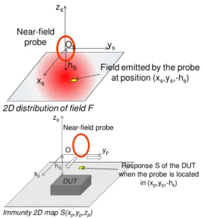
Let consider a near-field injection probe excited by a sinusoidal signal which produces a field F(xs,ys,zs) in any
point. The field (E or H field) is supposed known and undisturbed by nearby objects. For near-field injection on PCB or IC, we are only concerned by the distribution of the field F on a 2D horizontal plane (xs,ys) placed at a constant
distance or scan altitude hs below the injection probe (Fig. 1).
The result of a near-field injection scan on a DUT is a 2D immunity map which provides for each probe position (xp,
yp) placed at the scan altitude hs above the DUT its response
S to the near-field disturbance produced by the probe (Fig. 1). Each point of the map quantifies the effect of the disturbance produced by the probe on the DUT, when the probe is placed at this point. For example, the NFSI map can be the distribution of excitation of the probe to trigger a failure, or the induced voltage on the DUT. In this paper, S will be considered as the voltage induced on the DUT.
xs ys zs OS Near-field probe
hS Field emitted by the probe at position (xs,ys,-hs) 2D distribution of field F xp yp zp O DUT hS Immunity 2D map S(xp,yp,zp)
Response S of the DUT when the probe is located
in (xp,yp,-hs) Near-field probe
Fig. 1. Spatial distribution of the field F produced by the probe at a scan altitude -hS (top), immunity map of the DUT (bottom)
However, the immunity map provides an indirect and distorted picture of the coupling area of the incoming disturbance, because the probe produces a significant field over a large surface of the DUT. The spatial profile of the DUT response S is related to the field F by a DUT property called the receiving characteristic R. They are related by a convolution product as given in (1). The receiving characteristic of the DUT quantifies the response of the DUT to one particular component of the field F produced by the injection probe when it is placed in (xp,yp,-hs). The receiving
characteristic of the DUT is fully defined by the response to the six components of the magnetic and electric fields. It depends only on the geometrical and electrical properties of the DUT. It is independent of the radiating disturbance source if it does not affect the properties of a DUT. Thus, the spatial profile of the receiving characteristic of the DUT provides a direct information about the coupling area and the sensitivity of the DUT to the incoming field. As the near-field scan is performed on a finite number of points over the scan surface, a discrete convolution related S, F and R as shown in (2). The scan step must be smaller than the wavelength of the incoming disturbance to ensure that the DUT response to a local disturbance is characterized accurately.
(
)
(
)
(
p s p s)
(
s s)
s s p p p pdy
dx
y
x
F
y
y
x
x
R
y
x
F
R
y
x
S
∫∫
−
−
=
∗
=
,
,
,
,
(1)(
)
=
∑∑
(
−
−
)
(
)
k m m k j m i k j iy
R
x
x
y
y
F
x
y
x
S
,
,
,
(2)The determination of the DUT receiving characteristic is based on a discrete deconvolution process, which is done easily in spectral than in spatial domain. The transformation is based on the PWS theory. It consists in decomposing the field into a superposition of an infinite number of plane waves propagating in x and y directions with wave numbers kx and ky. The relation between spatial and spectral domain
representations of the field is ensured by a 2D Fourier transform in the xy plane, as given by (3) and (4) where subscript F~denotes the spectral domain representation.
(
)
∫ ∫
+∞(
)
∞ − − −=
F
x
y
z
e
e
e
dxdy
z
k
k
F
x y j t jk x jk y y x ω,
,
,
,
~
(3)(
)
=∫ ∫
−+∞∞(
)
x y y jk x jk t j y x k ze e e dk dk k F z y x F ω x yπ
, , ~ 4 1 , , 2 (4)With the spectral domain representation, (1) is rewritten in the following form. The receiving characteristic is the ratio between the DUT response and the field emitted by the probe. If the DUT response is expressed as a voltage, the receiving characteristic is expressed in m if the incoming field is electric, and in Ω.m if it is magnetic.
(
) (
(
)
)
z
k
k
F
z
k
k
S
z
k
k
R
y x y x y x,
,
~
,
,
~
,
,
~
=
(5)It should be underlined that the field, the DUT response and the receiving characteristic are complex figures. Consequently, the measurement of the phase of the field and the DUT response is required.
B. Principle of the extrapolation of radiated susceptibility The receiving characteristic is the main concept for the extrapolation of the radiated susceptibility to any other radiated disturbance source. The receiving characteristic of a DUT can be extracted after a NFSI experiment, according to (5). Examples are provided in [6] and [7].
In a general case, the DUT is illuminated by a radiating disturbance dominated by several components of electric and magnetic fields. The DUT response S can be separated in two contributions: the contribution of the E field coupling, and the one due to the H field coupling. Equation (1) can be rewritten according to the form shown in (6).
(
)
(
)
(
)
(
)
(
p p)
H p p E p p H p p E p py
x
H
R
y
x
E
R
y
x
S
y
x
S
y
x
S
,
,
,
,
,
∗
+
∗
=
+
=
(6) where SE and SH are the contributions of the E and Hfields to the DUT response. The vectors E and H contain the three components of the E and H fields. Vectors RE and RH
contains the receiving characteristics of the DUT to each of the three components of the E or H field, which has been extracted previously.
(
x
py
p)
[
E
x(
x
py
p) (
E
yx
py
p) (
E
zx
py
p)
]
E
,
=
,
,
,
(7)(
xp yp)
[
Hx(
xp yp) (
Hy xp yp) (
Hz xp yp)
]
H , = , , , (8)(
)
[
(
) (
) (
p p)
]
E z p p E y p p E x p p E y x R y x R y x R y x R , = , , , (9)(
)
[
(
) (
) (
p p)
]
H z p p H y p p H x p p H y x R y x R y x R y x R , = , , , (10)Once the spatial distribution of the incoming fields on the DUT is known, its response to this new radiated disturbance source can be predicted according to (6). An obvious
condition is to ensure that the DUT characteristic does not change between the NFSI test and this new radiating environment, and thus that the receiving characteristic is constant. Once again, this expression can be computed more easily in spectral domain according to PWS, as shown in (11). The spatial profile of the DUT response or immunity map to this new disturbance source is determined by a transformation from spectral to spatial domain according to (4).
(
)
(
)
(
x y)
H y x E y xk
R
E
k
k
R
H
k
k
k
S
~
,
=
~
.
~
,
+
~
.
~
,
(11)III. IMPLEMENTATION OF THE EXTRAPOLATION METHOD The first step consists in acquiring the immunity maps of the DUT to the different components the E and H fields. NFSI is a convenient method since the injection probe is placed in close proximity to the DUT. A maximum of six measurements based on six different injection probes are required to extract the receiving characteristics of the DUT to the six components of the E and H fields. The spatial distribution of the fields produced by the injection probes must be known. They can be determined by simulation or by near-field scan measurements based on calibrated near-field probes, as explained in [6]. In spectral domain, the voltages induced on the DUT during these six NFSI measurements (noted V1 to V6) can be expressed according to (12). In (15),
i k
F
~
is the E or H field component k produced by the injection probe during the ith NFSI measurement. Zero padding is required for the deconvolution process to avoid numerical issues related to the truncation of the field and NFSI distributions due to the finite surface of the scan.(
k
k
) (
F
k
k
)
R
V
~
x,
y=
~
x,
y.
~
(12) with:(
)
[
]
T y xk
V
V
V
V
V
V
k
V
1 2 3 4 5 6~
~
~
~
~
~
,
~
=
(13)(
)
[
H]
T z H y H x E z E y E x y xk
R
R
R
R
R
R
k
R
~
,
=
(14)(
)
=
6 6 6 5 5 5 4 4 4 6 6 6 5 5 5 4 4 4 3 3 3 2 2 2 1 1 1 3 3 3 2 2 2 1 1 1~
~
~
~
~
~
~
~
~
~
~
~
~
~
~
~
~
~
~
~
~
~
~
~
~
~
~
~
~
~
~
~
~
~
~
~
,
~
Hz Hy Hx Hz Hy Hx Hz Hy Hx Ez Ey Ex Ez Ey Ex Ez Ey Ex Hz Hy Hx Hz Hy Hx Hz Hy Hx Ez Ey Ex Ez Ey Ex Ez Ey Ex y xF
F
F
F
F
F
F
F
F
F
F
F
F
F
F
F
F
F
F
F
F
F
F
F
F
F
F
F
F
F
F
F
F
F
F
F
k
k
F
(15)The receiving characteristic R~ is determined by solving the linear system (12), for example by inverting the matrix
F~. In this paper, the extrapolation method will be applied on simulation results, which are not submitted to noise. Thus, solving (12) by a matrix inversion gives good results. However, the reduced signal-to-noise-ratio of measurement results may degrade the performances of this inverse filtering approach. Adequate noise filtering such as Wiener filtering and robust deconvolution process are required to overcome these limitations. These issues are not addressed in this paper.
The linear system in (12) requires 6 rows matrices which may be complex to build and sensitive to noise. It can be
simplified in some conditions. Depending on the geometry of the DUT, the coupling of some field components may be neglected. The associated terms of the vector R~are cancelled and less NFSI measurements are required to build this linear system. Moreover, if the H fields produced by electric field probe are neglected or, inversely, if the E fields produced by magnetic field probe are neglected, the extraction of RE and RH terms can be separated. This assumption is acceptable as long as the injection probes are electrically small.
Once the DUT receiving characteristic R has been extracted, the susceptibility to another radiating disturbance source can be extracted. It requires only the spatial distribution of the incoming fields produced by this new radiating source. If this source is placed in the near-field region of the DUT, the user certainly wants to predict the immunity map of the DUT, e.g. in order to identify interference-free placement. Equation (11) followed by a transform from spectral to spatial domain (4) can be used to predict the immunity map in this new configuration. If the source is placed in far-field region, the immunity map is not required since the illumination of the DUT is homogeneous. The prediction of the susceptibility of the DUT can be predicted directly by multiplying terms by terms the receiving characteristic and the incoming field distributions, as shown in (16).
(
)
(
)
∑∑
+
=
i j j i H j i Ey
x
H
R
y
x
E
R
S
.
,
.
,
(16)IV. CASE STUDIES
In this part, the extrapolation method is tested and validated through numerical case studies. A PCB trace is considered and the DUT response is the voltage induced at the end of the trace. In each case, six NFSI maps are computed based either on electric or magnetic dipoles, whose radiated field distribution is also determined. A NFSI map consist in the cartography of the voltage induced on line terminals for the different position of NF injection probe. Extrapolation of the immunity to another disturbance source based on the extraction of the receiving characteristic is done and then compared with a numerical simulation of the coupling between this new disturbance source and the DUT. Extrapolations of NFSI results are performed with Scilab [8]. A. Receiving characteristic of a short line
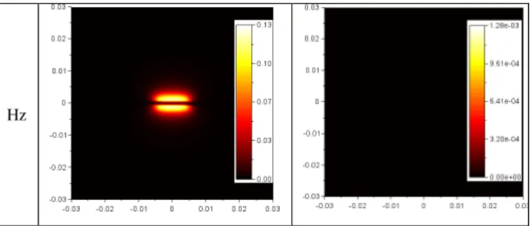
As a first example, a 10 mm long line routed at 1 mm above a ground plane and terminated at each end by 50 Ω resistors is considered. It is oriented along x axis. Its resistivity is neglected. Six NFSI maps are computed with six different injection probes: three electric field probes and three magnetic probes oriented along x, y or z axis, excited by a 300 MHz signal. They are moved above a 60 mm x 60 mm region at 2 mm above the line. The scan step along x and y axis is set to 1 mm. For each position of the injection probe, the voltage induced at one end of the line is recorded and plotted on one point of the NFSI map. The resulting maps of the injection done with the six different probes are shown in the second column of Table I.
The E and H fields produced by these six injection probes are also computed. According to (12), the receiving characteristics of the line under test to the different components of E and H fields are determined. They are
plotted in the third column of Table I. As the line couples only the z-component of the E field and the y-component of the H field, the receiving characteristics for the other field components are equal to zero.
TABLE I. COMPARISON BETWEEN NFSI AND RECEIVING CHARACTERISTIC MAPS OF THE STRUCTURE UNDER TEST
NFSI (in V) Receiving characteristics (in m or Ω.m) Ex Ey Ez Hx Hy Hz
The maps of receiving characteristics to Ez and Hy show a coupling area localized just above the line. As explained in [6], displaying immunity maps in terms of receiving characteristics provides a better spatial resolution and thus helps the identification of the coupling area of the incoming fields. Each point of the receiving characteristic map quantifies the contribution of the portion of DUT below the point to the coupling of the incoming field. A trivial case arises when a plane wave illuminates the DUT with a perpendicular incidence. Its phase is constant in the DUT plane, so the response is directly the sum of the product of the incoming field by the receiving characteristic measured above the DUT, as given by (16). The contribution of E and H field on the DUT susceptibility can be determined easily. For example, the receiving characteristic of the line to the z component of the E field is equal to 5.18×10⁻⁷ on the 10 points above the line. If the amplitude of the incoming Ez field is 1 V/m, the voltage induced by the electric field coupling on the line will be equal to 5.18 µV.
B. Extrapolation of radiated immunity from a near-field disturbance source
In a second example, the bended line described in Fig. 2 is considered. The line is 30 mm long and terminated by a 30 Ω resistor at one end, and 100 Ω at the other end. It is routed at 1 mm above a ground plane on a substrate with a relative electric permittivity of 4. As in the previous example, six NFSI obtained with six different injection probes are simulated. The scan area is also 60 mm x 60 mm with a scan step of 1 mm. The receiving characteristics are extracted according to (12). x y z 1.5 cm 1.5 cm 1 mm 2 mm Scan surface (60 x 60 mm)
Fig. 2. Case study: a bended line
The NFSI maps with a new near-field source placed at a different height can be predicted from the receiving characteristics. For example, let consider two cases: with an electric field dipole oriented along x-axis and with a magnetic field dipole oriented along z-axis, both placed at 10 mm above the line under test. The distribution of the fields produced by the dipoles that reach the line under test is first computed. Then, the NFSI maps are computed according to (11). They are compared with the result of the simulation of the coupling of both dipoles with the line under test. Both results are presented in Figs. 3 and 4. The comparison shows an excellent agreement between the results of the direct
simulation of the probe coupling to the line and the extrapolation from the NFSI done at 2 mm. The small differences are due to truncation of the scan surface of the DUT response and the field produced by the injection probe.
Fig. 3. NFSI map of the line under test with an Ex electric dipole placed at 10 mm: simulation of the coupling (on the left), extrapolation
from NFSI done at 2 mm (on the right)
Fig. 4. NFSI map of the line under test with an Hz magnetic dipole placed at 10 mm: simulation of the coupling (on the left), extrapolation
from NFSI done at 2 mm (on the right)
C. Extrapolation of far-field susceptibility
In a last case study, the radiated susceptibility of a 40 mm PCB trace to far-field disturbance is predicted from NFSI map results. The line is routed along x-axis at 1 mm above a ground plane with a relative electric permittivity of 4, and is terminated by 30 Ω and 100 Ω resistors at each end. As in the previous examples, six NFSI obtained with six different injection probes are simulated. The scan area is also 60 mm x 60 mm with a scan step of 1 mm. The receiving characteristics are extracted according to (12) at several frequencies between 10 MHz and 10 GHz.
Fig. 5. Far-field coupling on a PCB trace vs. frequency of the incoming plane wave: comparison between results of simulation of the far-field
coupling and extrapolation from NFSI
A 100 V/m vertically-polarized plane wave that propagates on the horizontal plane along x-axis is considered. From the receiving characteristics and the
distribution of this field along the line, the voltages induced on both ends of the line are determined according to (16). The evolution of these voltages vs. frequency is plotted in Fig. 5. These results are compared with those of direct simulation of far-field coupling on the line. They are in good agreement. The slight visible differences are also due to truncation of the scan surface of the DUT response and the field produced by the injection probe.
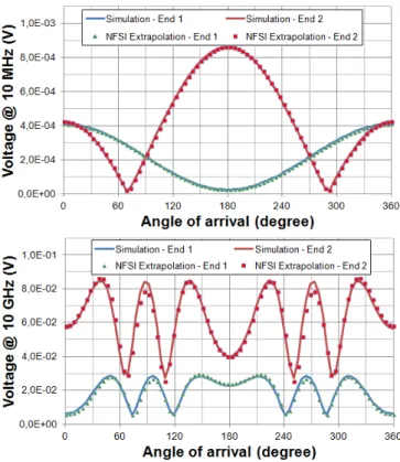
The same comparison between both simulation methods is also performed at two different frequencies (10 MHz and 10 GHz), but for different arrival angles of the electromagnetic wave in the horizontal plane. The results are presented in Fig. 6. As in the previous case, the correlation between the voltages extrapolated from NFSI and those calculated from the direct field to line coupling code is excellent.
Fig. 6. Far-field coupling on a PCB trace vs. angle of arrival of the incoming plane wave: comparison between results of simulation of the
far-field coupling and extrapolation from NFSI, at 10 MHz (top) and at 10 GHz (bottom)
The correct results provided by the extrapolation of radiated immunity from NFSI results prove the validity of the approach, for a disturbance source placed either in near-field or far-near-field region.
V. CONCLUSION
This paper has presented a post-processing method for results of near-field scan immunity, in order to predict the radiated susceptibility of a device under test whatever the nature and the position of the disturbance source. It is an important expectation from near-field scan as a prediction tool for PCB or IC. The approach proposed in this paper relies on the concept of receiving characteristic, which is an intrinsic property of the device under test. It does not depend on the incoming radiated disturbance. The receiving characteristic can be extracted from NFSI results and the
knowledge of the distribution of the E and H fields produced by the injection probe. Once the receiving characteristic has been extracted, the susceptibility of the DUT to any other radiated disturbance source can be predicted. One important suggestion from this paper is that NFSI results should be expressed in terms of receiving characteristics before analysis or exchange, since it reveals directly the contribution of E and H field coupling to the radiated susceptibility of the DUT.
In this paper, only simulation results were treated with the method in order to prove its validity from a theoretical point of view. However, the practical use of this method is not as straightforward because of the number of measurements to be done. As suggested in this paper, some assumptions can be provided to reduce the number of measurements. They are valid as long as the injection probes remain electrically small. Another practical aspect which was not taken into account in this study is the contribution of noise which affects any measurements. Adequate filtering and robust deconvolution techniques are thus required to limit its effect on the receiving characteristic extraction. Further works will be done to adapt the method to measurement case studies and prove its robustness. Finally, another difficulty from a practical point of view is the extraction of phase information. The method requires complex values and thus the phase of the incoming field and the DUT response. The first one can be obtained from experiments or simulations with a good accuracy. Depending on the equipments used during NFSI measurement and the nature of the DUT response, the measurement of the phase may be impossible. Future works should analyze the
influence of the lack of phase information on radiated susceptibility extrapolation, and test different methods of phase estimation.
REFERENCES
[1] S. Zaky, K.G. Balmain, G.R. Dubois, “Susceptibility Mapping”, in Proc. Int. Symp. on EMC, 1992, pp. 439-442.
[2] O. Kroning, M. Krause, M. Leone, "Near field-Immunity Scan on Printed Circuit Board Level", in Proc. SPI, 2010, pp. 101-102. [3] A. Boyer, E. Sicard, S. Bendhia, « Characterization of the
Electromagnetic Susceptibility of Integrated Circuits using a Near Field Scan », Electronic Letters, vol. 43, no. 1, pp. 15-16, 4th Jan. 2007.
[4] T. Dubois, S. Jarrix, A. Penarier, P. Nouvel, D. Gasquet, L. Chusseau, B. Azaïs, " Near-Field Electromagnetic Characterization and Perturbation of Logic Circuits", IEEE Trans. on Instrumentation and Measurement, vol. 57, no. 11, pp. 2398 - 2404, Nov.2008.
[5] G. Muchaidze, J. Koo, Q. Cai, T. Li, L. Han, A. Martwick, K. Wang, J. Min, J. L. Drewniak, D. Pommerenke, "Susceptibility Scanning as a Failure Analysis Tool for System-Level Electrostatic Discharge (ESD) Problems", IEEE Trans. on EMC, vol. 50, no. 2, pp. 268-276, May 2008.
[6] A. Boyer, M. Cavarroc, "Improvement of the Spatial Resolution of Near-Field Immunity Maps", EMC Compo 2015, Edimburgh, Scotland, November 2015.
[7] A. Boyer, " Improving Spatial Resolution of Immunity Maps by Post-Processing", 2016 Asia-Pacific International Symposium on Electromagnetic Compatibility and Signal Integrity, May 18 – 21, 2016, Shenzhen.
[8] Scilab v6.0, Open source software for numerical computation, www.scilab.org.