AC Coupled Ripple Reduction Method for
Chopper-Stabilized Amplifiers
by
Alex R. Sloboda
S.B. Electrical Science and Engineering
Massachusetts Institute of Technology, 2017
Submitted to the Department of Electrical Engineering and Computer
Science
in partial fulfillment of the requirements for the degree of
Master of Engineering in Electrical Engineering and Computer Science
at the
MASSACHUSETTS INSTITUTE OF TECHNOLOGY
June 2018
@ Alex R. Sloboda, 2018. All rights reserved.
The author hereby grants to MIT permission to reproduce and to
distribute publicly paper and electronic copies of this thesis document
in whole or in part in any medium now known or hereafter created.
Signature redacted
A uthor ...
Department of Electrical Engineering and Computer Science
Certified by....
Certified by...
May 25, 2018
Charles Sodini
LeBel Professor of Electrical Engineering
Faculty Thesis Supe;vior
...
Signatufre redacted
Greg DiSanto
Design Engineer, Analog Devices Inc
Signature redacted
Accepted by
MASSACHSMSIN~SY1WE
Ajj 20
2018
Company Thesis Supervisor
Katrina LaCurts
Chair, Master of Engineering Thesis Committee
Sianature redacted
AC Coupled Ripple Reduction Method for
Chopper-Stabilized Amplifiers
by
Alex R. Sloboda
Submitted to the Department of Electrical Engineering and Computer Science on May 25, 2018, in partial fulfillment of the
requirements for the degree of
Master of Engineering in Electrical Engineering and Computer Science
Abstract
There exists a variety of applications where precision voltage amplifiers are re-quired to faithfully sense and properly filter signals. While methods have been devel-oped to create such precision amplifiers, these methods typically suffer from increased output noise. In the case of chopper amplifiers, this increased output noise comes in the form of narrow bandwidth, high frequency noise referred to as ripple noise. To reduce this ripple noise many topologies and techniques have been created and put into practice. However all of these topologies and techniques come at some cost in larger circuit area, higher power consumption, or increased noise. An AC coupled ripple reduction filter for chopper-stabilized precision amplifiers has been developed to reduce the cost of filtering out ripple noise. What follows is an explanation of ripple noise, an examination of existing ripple reduction methods, the presentation of the AC coupled ripple reduction filter, and simulated evidence of improved performance with this new method over existing methods in terms of smaller area, lower power consumption, and reduced noise.
Faculty Thesis Supervisor: Charles Sodini Title: LeBel Professor of Electrical Engineering Company Thesis Supervisor: Greg DiSanto Title: Design Engineer, Analog Devices Inc
Acknowledgments
I would first like to thank my company supervisor, Greg DiSanto, for his amazing guidance and mentorship. This project only came about because he gave me the freedom and support to explore my own ideas and the know-how to properly test and implement them.
I would like to thank the many talented engineers at Analog Devices who helped me along the way including: Andy Roberts, John Fiorenza, Lance Bourque, Jeff Cox, Adam Shou, Erjon Qirko, and Joseph Petrofsky.
I would like to thank Professor Sodini for agreeing to be my faculty thesis super-visor despite having never met me before. His feedback and expertise, as well as his familiarity with industry research, has been invaluable in creating this thesis.
I would like to thank all of my incredible friends, TA's, lecturers, and professors for helping me survive, grow, and thrive at MIT these past five years.
Finally I would like to thank my family for their endless encouragement, love, and support in all of my endeavors.
Contents
1 Introduction
1.1 Desired Amplifier Characteristics . . .
1.2 Transistor Comparison and Tradeoffs
1.3 Role of Precision Amplifiers Today .
1.4 Operational Amplifier Offset, Drift and
2 Dynamic Offset Reduction Techniques
2.1 Auto-Zeroing . . . .
2.2 Chopping . . . .
3 Chopper Ripple Reduction Techniques
3.1 Low Pass Filter . . . .
3.2 Switched Capacitor Notch Filter . . . .
3.3 Ripple Reduction Feedback Loop . . .
3.4 Comparison of Existing Methods . . .
1/f Noise...
4 Proposed AC Coupled Ripple Reduction Topology
4.1 New M ethodology . . . .
4.2 Implementation and Simulation of New Methodology . . . .
4.3 Comparison With Existing Ripple Reduction Techniques . . . .
5 Conclusions 5.1 Summary of W ork . . . . 5.2 Future W ork . . . . 9 9 10 11 12 15 15 17 24 24 . . . . 26 29 . . . . 30 32 32 36 40 42 42 42
List of Figures
1-1 Model of Input Offset Voltage . . . . 12
1-2 Model of Operational Amplifier Input Referred Noise . . . . 13
1-3 Models of Input Offset Voltage and Input Referred Noise (a) and Out-put Offset Current and OutOut-put Referred Current Noise (b) of InOut-put Stage Transconductance . . . . 14
2-1 Sampling an Amplifier's Offset (a) and Correcting the Sensed Offset (b) Using the Auto-zeroing Technique . . . . 15
2-2 Noise Spectral Density of Amplifier With and Without Auto-zero Noise Folding . . . . 17
2-3 Input Signal (1kHz "White" Input) (a) and 1/f Noise Spectra (b) . . 18
2-4 Example Output Signal Spectra in the Presence of 1/f Noise Without C hopping . . . . 19
2-5 Example Output Signal Spectra in the Presence of 1/f Noise With Chopping Before Demodulation (a) and After Demodulation (b) . . . 19
2-6 Block Diagram of Chopper Amplifier Topology . . . . 20
2-7 Chopping of Input Signal and Modulation of 1/f Noise . . . . 21
2-8 Block Diagram of Chopper Stabilized Amplifier Topology . . . . 22
3-1 External Ripple Reduction Low Pass Filter . . . . 24
3-2 Internal Ripple Reduction Notch Filter . . . . 26
3-3 Effect of Switched Capacitor Notch Filter on Output Offset Current of Input Stage Transconductance . . . . 27
4-1 Proposed Ripple Reduction Topology . . . . 32
4-2 Block Diagram Implementation of Proposed AC Coupled Ripple
Re-duction Filter . . . . 33
4-3 Example Clocking Diagram for AC Coupled Ripple Reduction Technique 35
4-4 Monte Carlo Transient Simulations of Proposed AC Coupled Ripple
Reduction Filter . . . . 37
4-5 Ripple in Monte Carlo Transient Simulations . . . . 37
4-6 Input Referred Noise Spectrum of Chopper Amplifier Without Ripple Reduction Filter (Green), With Switched Capacitor Ripple Reduction
List of Tables
3.1 Comparison of Existing Ripple Reduction Techniques . . . . 31
4.1 Comparison of AC Ripple Reduction Filter and Existing Ripple
Chapter 1
Introduction
Before the problem of output ripple in precision amplifiers, and the various tech-niques that have been developed to combat it, can be discussed in detail it is important to first examine the design process and constraints that have led many precision am-plifier designs to exhibit ripple. This examination will begin by detailing the desired characteristics of these amplifiers and the limitations of the devices that come to make them up.
1.1
Desired Amplifier Characteristics
The efficient and accurate measurement and processing of analog signals is crucial in the modern world. A common tool widely used in electronic systems for
perform-ing measurements and processperform-ing signals is the operational amplifier [1]. Operational
amplifiers are active electronic devices composed of transistors and passive compo-nents. What makes them so useful for making measurements on analog signals is their extremely high gain which amplifies small sensed differential signals by many orders of magnitude. Additionally, operational amplifiers meant for measuring volt-age signals possess very high input impedances, which allow for measurement without perturbing the measured signal, and low output impedances, which result in a robust output signal. There also exist operational amplifiers designed to measure and output current signals which have the opposite input and output impedance configuration.
This thesis will focus on voltage input voltage output operational amplifiers.
In most applications, regardless of the type used, the output of the operational amplifier is passed through an appropriate negative feedback network back to the input. In such a configuration, a designer is able to leverage the massive gain of the operational amplifier to produce very precise amplified and filtered versions of the input signal [2]. In addition to the large gain, high input impedance, and low output impedance that characterize general voltage mode operational amplifiers other important specifications relate to the speed, accuracy, and power consumption of these devices. Ideally an amplifier could operate instantaneously with no discernible offsets while drawing no power [3]. While amplifiers can be built which closely approximate some of these goals, an ideal amplifier is impossible to create.
1.2
Transistor Comparison and Tradeoffs
For many years bipolar junction transistors (BJTs) were the device of choice in analog circuit designs for building operational amplifiers. Metal-oxide-semiconductor field effect transistor (MOSFET) process technology had not yet advanced enough to provide consistent and adequate levels of amplification and high frequency perfor-mance for analog systems [3]. As a result, those operational amplifiers designed with bipolar processes were able to achieve higher gains, higher speeds, lower offsets and lower noise than those designed with FETs. Today, however, FET processes have advanced to the point that both types of devices are viable options, and are even mixed, depending on the desired system performance goals.
Despite the fact that both types of transistors are now viable analog building blocks they still possess their own strengths and weaknesses. BJTs are often found in precision operational amplifier circuits as it is possible to trim them for low absolute offsets and low offset drift simultaneously, resulting in long term precision devices. This is due to their exponential, PTAT current characteristic as well as their typically larger transconductances that together work to keep the input pair matched over a wide range of temperatures and operating conditions. On the other hand it turns out
that MOSFET based operational amplifiers are not as easily trimmed for both low offsets and low offset drift. Trimming a MOSFET based amplifier to zero offset at a given bias point does not simultaneously result in a low drift component. Therefore trimming must be performed at at least two bias points or temperatures in order to significantly reduce the drift component. Even after performing multiple trimmings, MOSFET based amplifiers still exhibit higher levels of offset and drift than their BJT counterparts since MOSFETs have lower transconductances and quadratic current characteristics when operated in strong inversion. What then makes the MOSFET appealing for analog design is its ability to be biased properly using very low voltages and currents compared to the BJT [4]. As a result of this low-power property, it is of-ten worth the effort to use MOSFETs in conjunction with additional offset correction or cancellation techniques when power consumption is a pressing concern.
1.3
Role of Precision Amplifiers Today
Precision amplifiers are essential in many modern sensor and communication sys-tems. These amplifiers provide both increased resolution and dynamic range by ac-curately and precisely detecting and processing sensitive signals with amplitudes on the order of microvolts. In addition, they maintain consistent measurements across a broad range of operating conditions. As a result these amplifiers can perform high resolution sensing on a wide range of variables including ambient temperatures, biomedical signals, and gas concentrations enabling further data conversion and signal processing.
As modern sensor systems have become more common, and remote sensing more popular, the power requirements on amplifiers have become more stringent. In re-sponse, despite their poor inherent precision performance, it is becoming more com-mon that precision amplifiers are being designed using MOSFETs as the primary building block instead of BJTs. In order for these low-power MOSFET based ampli-fiers to achieve the required levels of precision, circuit techniques have been developed to dynamically cancel or filter out the offsets and low frequency drifts associated with
these devices that manufacturer trimming is not able to completely eliminate.
1.4
Operational Amplifier Offset, Drift and 1/f Noise
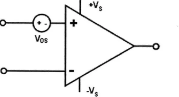
Vos
Figure 1-1: Model of Input Offset Voltage
Before examining the particular techniques used to remove offset and low fre-quency noise it is important to understand what these defects are as well as how and why they manifest themselves in operational amplifiers. The offset of an amplifier is the apparent applied differential input voltage to the amplifier when there is no differential voltage being applied to the input. It is often represented by an apparent voltage source located at one of the inputs of the amplifier as depicted in Figure 1-1 [2]. Input offset can be the result of a variety of factors but primarily results from systematic asymmetry in the circuit design and random device mismatch. While a designer can ensure that a circuit does not possess any systematic offset resulting from asymmetries in the design, there will always be some levels of mismatch in real devices due to manufacturing variations. Smart choices of device sizes and topologies can reduce the magnitude of this mismatch and its impact on the overall system, but all op-amps inevitably exhibit some level of offset.
Offset drift refers to how the offset of an amplifier changes. Drift can be mea-sured with respect to applied input common mode voltages, power supply voltages, temperatures, and even time. A major contributor to drift, much like offset, is the mismatch of devices in the amplifier. As non-identical devices are placed in different biasing conditions, their behaviors will not directly track one another resulting in
greater or lower amounts of offset compared to their initial condition. While it can appear apparently random, offset drift is deterministic and a function of the amplifiers operating conditions. If operating conditions were held constant across the entirety of the amplifier and devices were noiseless, the offset would not drift.
Vn
Figure 1-2: Model of Operational Amplifier Input Referred Noise
Another significant apparent, but fundamentally different, contributor to drift is low frequency flicker, or 1/f, noise. Flicker noise affects all transistors and causes apparent offset drift due to its high spectral density at low frequencies. What makes flicker noise especially troublesome is that even if operating conditions are held con-stant it affects the offset of an amplifier since it is a random process. The fact that its power spectral density is proportional to the inverse of frequency also makes it
very difficult to filter out when signals of interest have low frequency components [4].
Figure 1-2 represents a model of flicker noise where it appears as a single AC voltage noise source at the input of the amplifier.
-- iout gm*(+V)
-gml gml
(a) (b)
Figure 1-3: Models of Input Offset Voltage and Input Referred Noise (a) and Output Offset Current and Output Referred Current Noise (b) of Input Stage
Transconductance
A multistage amplifiers input offset and low frequency noise are typically domi-nated by the offset and low frequency noise of the first stage. This is because the offsets of later stages are attenuated by the gain of the first stage once the amplifier is put into feedback. As a result, the offset and noise of an amplifier is typically approx-imated as the offset and low frequency noise of the first stage. This can be modeled in the following two ways: as a DC voltage source and AC voltage noise source in series with the input of the first stage or a DC current source and AC current noise source in parallel with the output of the first stage. These models are equivalent, in fact the voltage and current differ only by a factor of the input transconductance, and both are depicted above in Figure 1-3. These models will be useful to look back upon as techniques to remove offset and 1/f noise are examined.
Chapter
2
Dynamic Offset Reduction
Techniques
In contrast to manufacturer trimming which is only performed once in the am-plifier's lifetime, dynamic offset reduction techniques aim to remove the offset, offset drift, and flicker noise of an amplifier by continually measuring the low frequency be-havior of the amplifier itself and correcting for it. This chapter examines two popular techniques used to carry out dynamic offset reduction, auto-zeroing and chopping.
2.1
Auto-Zeroing
+ VC=V05 1 Vas,v$
M V
_
Vc=
Vos VO0 VIN(a) Sampling Phase
+
(b) Correction Phase
Figure 2-1: Sampling an Amplifier's Offset (a) and Correcting the Sensed Offset (b) Using the Auto-zeroing Technique
Auto-zeroing is a technique capable of reducing the input offset and drift of an amplifier [5]. Auto-zeroing involves temporarily removing the amplifier from the main signal path in order to regularly sample its offset. This sampled offset is then sub-tracted from the input of the amplifier in order to cancel it out. An example of a possible, ideal implementation of auto-zeroing is shown in Figure 2-1. As described there are two phases, the sampling phase and the correction phase. During the sam-pling phase the amplifier is put into unity gain feedback while its non-inverting input is attached to some fixed voltage, in this case ground. A capacitor between the two inputs samples the resulting differential input voltage directly. Once this differen-tial voltage has been sampled, the amplifier is put back into its normal amplifying configuration and the sampled voltage is put in series with the non-inverting input. Assuming that the gain of the amplifier is sufficiently large, the sampled voltage will be equal to the input offset voltage and will directly cancel out the offset of the amplifier.
This sampling and correction occurs at some regular auto-zero frequency in order to accurately correct for the offset as it varies with operating conditions, for flicker noise, and for capacitive discharge of the sampled offset. One clear issue with this particular implementation is that it cannot be used in continuous time systems since the amplifier is regularly taken out of the signal path in order to have its offset sampled. This would result in periods of discontinuity which cannot be tolerated in many applications.
If continuous operation is required the above auto-zero method can be improved upon by using two amplifiers [5]. At any given time one amplifier will be in the main signal path while the other is in the sampling configuration. They can then be swapped simultaneously preventing significant discontinuities beyond charge injection glitches. A downside to this modified method is that the power consumption and area of the auto-zeroed amplifier is now approximately double that of the original since two entire amplifiers are involved. Thus, for continuous applications where low power and area are crucial, this auto-zero technique can be difficult to successfully implement.
unauto-zeroed noise
auto-zeroed noise
2fAz
f
Figure 2-2: Noise Spectral Density of Amplifier With and Without Auto-zero Noise
Folding
Beyond power and area concerns, another issue brought about when auto-zeroing is performed is that the sampling process results in noise folding. Broadband noise from higher frequencies folds into the DC to auto-zero frequency bandwidth and effectively raises the white noise level of this region [6]. So while offset and 1/f noise are successfully removed, meaning the amplifier does have significantly reduced low-frequency error, auto-zero amplifiers typically exhibit significantly higher levels of white noise in the low frequency region compared to the original amplifier. A rough
approximation of this effect can be seen in Figure 2-2 where fAz represents the
auto-zero frequency. A more detailed analysis of this phenomenon was completed by Enz and Temes in [5].
2.2
Chopping
Chopping is another technique that can result in a low offset, low drift amplifier by using frequency modulation and filtering rather than sampling [5]. In this technique the input signal to the amplifier is first modulated to a higher frequency, called the chopping frequency. Both the modulated input signal and the unmodulated offset and noise characteristics of the first stage are then amplified. Following amplification, the input signal is modulated back down to its original frequency while the offset and low frequency noise are modulated up to the chopping frequency where they can be filtered out without effecting the amplified input signal.
Input Signal Power Spectral Density
V
5r
10 10 102 101 1 , ,05 1 Frequency (a)1/f Noise Power Spectral Density
10 102 101
Frequency (b)
Figure 2-3: Input Signal (1kHz "White" Input) (a) and 1/f Noise Spectra (b)
To best understand this process it is helpful to look at power spectral density plots.
Above in Figure 2-3 the spectral densities of an example 1 kHz bandwidth white input
signal (a) and 1/f noise source (b) are plotted respectively. The input signal has a
uniform power spectral density of 1
Vup to 1kHz while the spectral density of the
7Hz
1/f noise source is equal to 1
at 1 Hz and falls off from there as expected. Note
that the 1/f noise spectral density will approach infinity as f approaches 0 but, for
the purpose of making legible plots, the frequency spectrum will only be plotted for
frequencies greater than 1 Hz and the maximum spectral density of noise will be
limited to 1
Vwhen relevant. White noise is not featured in the plots as chopping
7H-z
does not have the significant noise folding effects on white noise that auto-zeroing
exhibits.
N
I.
E CL 0 5-to > 0* 05 100 101 102 103 10" 105 Frequency
Figure 2-4: Example Output Signal Spectra in the Presence of 1/f Noise Without Chopping
If the input signal from Figure 2-3 (a) was to be input into a non-chopped amplifier with the noise characteristic of Figure 2-3 (b), the resulting output signal would have a spectral density of the form depicted in Figure 2-4. Here we see the output spectral density is equal to the root sum of squares of the two individual spectrum since the noise and input signal are uncorrelated. It can be clearly seen that the 1/f noise would significantly distort the lower frequency portion of the input signal in this situation.
12 1.21
2a 0
OC
Frequency Frequency
)(b)
Figure 2-5: Example Output Signal Spectra in the Presence of 1/f Noise With Chopping Before Demodulation (a) and After Demodulation (b)
In Figure 2-5 (a) the same 1kHz "white" input signal has been used but it has been modulated prior to amplification using the chopping technique with a chopping frequency of 20 kHz. As a result, the bandwidths of the input signal and low frequency noise have no significant overlap. Figure 2-5 (b) depicts the resulting output signal once the input signal has been demodulated back to its original frequency. In the process of demodulating the input signal the 1/f noise is modulated up to the chopping frequency where it can be readily distinguished from the actual input signal of the amplifier and filtered. Though the modulated 1/f noise is shown to reach a maximum
magnitude of 1
,
it should ideally reach infinity at exactly the chop frequency sincethe power spectral density of the noise before modulation was infinite at 0 Hz. This is not depicted in order to make the plots legible.
cc's CC2
+
I+
ChOpI G ChDp2 cciT TIM OUW Stage
Modulated Vin
Vi n
chos4
Vin
Modulated Vin + Amplified Vin +
1/f Noise Modulated 1/f Noise
ckop2
1/f Noise
Figure 2-7: Chopping of Input Signal and Modulation of 1/f Noise
The block diagram in Figure 2-6 is one example of a possible implementation of the chopping technique. Here the chopping switches, depicted by the blocks Chopi and Chop2, surround the input stage transconductance modulating its low frequency offset and noise up to the chopping frequency as depicted in Figure 2-7. The following stages serve to further amplify the input signal and, so long as their bandwidths are low enough, low-pass filter the modulated offset and noise. There might be concern about the offsets and 1/f noise present in the second and output stages. As long as the first stage has enough gain these defects will be attenuated to acceptable levels once the amplifier is placed in feedback. Other topologies place multiple stages in between the chopping switches to attenuate later stage noise and offset contributions when the gain of the first stage is insufficient and it is not feasible to increase it.
A significant issue with the chopping amplifier as described so far is that it must have a chopping frequency significantly higher than the bandwidth of the input signal to work properly [6]. If it does not, the modulated noise will remain in the bandwidth
of the input signal and will distort higher frequency inputs to the amplifier, manifest-ing itself as triangular output ripple due to the finite bandwidth of the amplifier. The chopping frequency can be increased to lessen these effects but doing so causes the input impedance and input bias current characteristics of the amplifier to deteriorate. Since these input characteristics are crucial in many precision sensing amplifications, changes to this topology must be made in order to achieve higher bandwidths.
i!
CC1 CCU
+~
-TI+
ChOPI GMI Chop2
CT
G2 C2 tOSbFigure 2-8: Block Diagram of Chopper Stabilized Amplifier Topology
The amplifier topology shown in Figure 2-8, called a Chopper Stabilized Amplifier topology, seeks to solve the low-bandwidth problem of the previous chopper design [6]. To accomplish this goal, this amplifier possesses two signal paths: a high frequency path consisting of the transconductance gm-ff and an output stage, and a low fre-quency path consisting of the transconductances gml and gm2 and an output stage. Both paths share the output stage as well as a common input. The low frequency path is responsible for amplifying DC and low frequency input signals. It also serves to remove any offset or flicker noise from the amplifier using the chopping technique described earlier combined with compensation that causes it to have a high gain, but a bandwidth significantly lower than the chopping frequency. The high frequency path has a lower DC gain than the low frequency path but a much larger bandwidth
and thus does not affect the overall system input-output characteristics until the gain of the low frequency path has rolled off sufficiently. As long as the frequency com-pensation for both paths is properly chosen the overall system can be made to have a transfer function extremely similar to that of a single pole operational-amplifier, but without significant offset or low frequency noise.
The advantages of chopping over auto-zeroing are seen primarily in continuous time circuits where chopper amplifiers require less area and power consumption and have less low frequency noise. Where auto-zeroing requires two amplifiers in order to cancel offset and provide continuous time operation, chopping only requires an additional feed-forward stage to be added to the amplifier in order to cancel offset and achieve high bandwidths. Since chopping does not involve sampling it does not exhibit the same noise folding behavior of auto-zeroing. Rather, chopping modulates low frequency offset and noise up to the chopping frequency resulting in the high frequency noise characteristic depicted earlier. White noise at higher frequencies is also modulated down to low frequencies which may bring up concerns that chopping does actually cause noise folding. However, since the low frequency noise is simul-taneously modulated up to the chop frequency the noise is simply swapped rather than summed. The noise that is modulated to high frequencies then exhibits itself as ripple at the output of the amplifier after being filtered by the bandwidth of the amplifier. In the next section techniques will be examined that attempt to reduce or remove this ripple noise.
Chapter 3
Chopper Ripple Reduction
Techniques
As discussed in chapter 2, chopping is a powerful technique capable of significantly reducing offset and 1/f noise in an amplifier by modulating these defects up to a higher chopping frequency. Amplifiers that use chopping are often distinguishable by their high frequency ripple noise which can be undesirable in many applications. In this chapter existing ripple filtering techniques are examined and compared to understand their benefits and the tradeoffs associated with using them.
3.1
Low Pass Filter
L
T
One method to reduce the amplitude of ripples resulting from chopper offset can-cellation involves using a low pass filter like that shown in Figure 3-1. In practice such a filter is typically either provided by the user and is built out of discrete pas-sive components to suit the particular needs of the users system or is built into the compensation for the low frequency path if the amplifier is using a chopper-stabilized topology [7]. In either case these filters are typically only first or second order low pass filters and thus exhibit slow roll offs of 20 or 40dB per decade respectively.
This slow roll off produces many issues. If the filter is constructed by the user using discrete passive components this filter may require severely limiting the bandwidth of the whole amplifier in order to reduce the ripple sufficiently for precision sensing applications which may be dealing with microvolt level input signals. Even if a low bandwidth is acceptable, such a filter may require large discrete components increasing the overall size of the system. Similarly, if the roll off is achieved through the design of the amplifier, it can be very difficult to attenuate the ripple enough to reduce the noise power below that of microvolt level input signals. For this reason, while some level of low pass filtering is often done within the low frequency path of the amplifier, it is typically used in conjunction with another technique to further reduce the magnitude of ripple.
3.2
Switched Capacitor Notch Filter
CC2
Vo~
Figure 3-2: Internal Ripple Reduction Notch Filter
Recognizing that the ripple is often found within a very small bandwidth around the chopping frequency, another approach to removing the ripple from the output involves implementing a notch filter at the chopping frequency rather than a low pass filter. Implementing such a notch filter external to the amplifier is very difficult to do as the notch must be carefully centered on the chopping frequency which can vary over time and temperature. However, an integrated notch filter has the advantage of having access to the chopping clock and thus, if implemented using switched ca-pacitors, can be directly synced with the clock. Topologically, such a filter would be located as shown in Figure 3-2.
Ui
CCs
IDS Iripple
C-intA
Vripple
Figure 3-3: Effect of Switched Capacitor Notch Filter on Output Offset Current of Input Stage Transconductance
Engineers at Texas Instruments invented such a switched capacitor notch filter for reducing ripple in chopper amplifiers [8]. A diagram of their design is shown in Figure 3-3. This design chooses to implement the notch filter directly after the input stage and second chopper of the amplifier. Here a capacitor, C-intA, integrates the modulated offset current produced by the input stage. This capacitor remains in place during half of each chopping phase. As a result the offset current from the first stage, which switches direction during each chopping cycle, integrates to a net zero charge and thus zero voltage while the capacitor is in place. Another identical integrating capacitor, C-intB, which had been located at the input of the second stage is then swapped with C-intA. In this manner, the C-int capacitors shuffle charge from the first stage to the input of the second stage. By switching the integrating capacitors ninety degrees out of phase with the chopping clock, only the input signal is able to
C-intB
Cout
Vout
pass from input to output unfiltered while the offset is completely cancelled.
In theory, given only offset as a nonideality in the amplifier, this notch filter would perfectly remove any and all offset ripple. In reality, due to other nonidealities such as clock skew and charge injection, the cancellation is not perfect but still has been shown capable of reducing ripple by over 60dB. The large levels of attenuation possible combined with the low area and power required for implementation make this an extremely attractive method for reducing ripple.
That being said it is not without its problems. By placing an integrating and charge shuffling block after the first stage of the amplifier rather than a continuous signal path, the low frequency path suffers from additional phase lag. While the overall amplifier transfer function can be made stable through the use of a high frequency path as discussed earlier, this phase shift will still significantly reduce the phase margin of the local loop that compensates the low frequency path. The reduced phase margin will amplify noise and manifest itself as a bump in the overall input referred noise characteristic of the amplifier.
Another issue is that the designer has little control over the bandwidth of this notch filter. The notch is a result of the anti-symmetry of the modulated offset signal from the first stage causing it to cancel itself out when integrated over half of two chopping cycles as depicted in Figure 3-3. However when the offset is varying with time, or when the signal to be filtered is the modulated 1/f noise of the first stage, this anti-symmetry begins to break down and some amount of noise will pass through. For those devices which possess high 1/f corners it may be desirable to increase the bandwidth of this filter to better attenuate modulated noise but that is not possible with this filter without increasing the chopping frequency.
3.3
Ripple Reduction Feedback Loop
ChopI
Gu Chop2Chopib
Figure 3-4: Block Diagram of Ripple Reduction Feedback Loop
One more existing method for reducing chopping ripple is depicted in Figure 3-4. This technique uses a ripple reduction feedback loop to reduce the level of output ripple [6]. This works by AC coupling the voltage at the output of the second stage back into a local feedback stage. This stage has its own chopper which is synced with the choppers in the main path. As a result, the ripple that couples in is modulated back down to DC from the chopping frequency while input signals are modulated to higher frequencies. The transconductance Gmfb1 then integrates this signal in order to amplify the DC offset portion. Another transconductance, Gmfb2, then uses this amplified offset to produce a corrective offset current that counteracts the offset current of the input stage transconductance significantly reducing the amplitude of output ripple.
By using an active feedback stage to reduce the magnitude of ripple the designer has a flexibility in choosing the bandwidth and magnitude of attenuation. If the input stage has a high 1/f noise corner the ripple reduction loop can be made to have large bandwidth to counteract these problems quickly. Also, if the worst case and desired magnitudes of ripple of the amplifier are known the designer can increase or decrease
the gain of the feedback stage appropriately to trade off ripple reduction with power consumption.
While this technique offers great flexibility, it comes at a price. Additional transconductances must be implemented in order to filter out ripple and these stages will require increasing the power consumption and area of the original amplifier. Care must also be taken to ensure that the local feedback loop created is properly compen-sated and stable which may conflict with ripple magnitude reduction and bandwidth goals.
3.4
Comparison of Existing Methods
Shown in Table 3.1 is a comparison of these existing methods of chopper ripple reduction. The strengths and advantages of each method are highlighted in green while issues with each method are highlighted in red. It is from this comparison of existing topologies that an opportunity for a new topology was recognized. It was important that this new topology not introduce any additional defects that would make it undesirable as a signal amplifier. Based on careful analysis of existing ripple reduction methods, and with these concerns in mind, a new topology was created with the intent of matching or outperforming performance in the areas of ripple
Method
Ripple At-
Area
Power
Filter
Additional
tenuation ___Bandwidth_ notes
Low Pass
First order
Increases
Low to
Low
Often
im-Filter
roll-off
signifi-
none
frequency
plemented
cantly with
cutoff
alongside
filter order
controllable
other
methods
Infinite
ideally
60dB
reported
Designable
ideally
60dB
reported
Low
1-2
additional
gm stages
Low to
none
1-2
additional
gm stages
Determined
by
chopping
freauency
Poor phase
margin in
LF path
Local loop
must be
compen-sated
Table 3.1: Comparison of Existing Ripple Reduction Techniques
SC Notch
Filter
Ripple
Reduction
Chapter 4
Proposed AC Coupled Ripple
Reduction Topology
4.1
New Methodology
CpCI CO
Figure 4-1: Proposed Ripple Reduction Topology
Another approach to filtering out offset and flicker noise is depicted by the block diagram shown in Figure 4-1. Here we find a block diagram identical to that of the switched capacitor notch filter of Figure 3-2 but here the ripple filter instead lies
between gml and the Output Chop rather than between the Output Chop and gm2. Since the ripple filter now precedes the Output Chop, the offset and low freuqency noise it encounters from the first stage transconductance is the unmodulated offset and flicker noise of the first stage. This offset and noise, since it has not been modulated by the Output Chop, is still at DC and low frequencies respectively. Meanwhile, the low frequency input to the amplifier has already been modulated to the chopping frequency by the Input Chop. The spectra of these signals at the various locations in the amplifier are displayed in Figure 2-3.
With these spectra in mind it is clear that this ripple filter implementation should be designed to act as a high pass filter rather than a notch or low pass filter in order to remove the undesired low frequency offset and noise from the input stage before they propagate to the output as ripple while leaving the overall input signals to the amplifier unattenuated. Since this filter couples the desired high frequency signal to the second stage while blocking the low frequency noise and DC offset of the first stage it will be referred to as the AC coupled ripple reduction filter.
__
+
gml--
F---Al
Vint CS Integration Phase++
vint cs
gmc
- Shuffle Phase Output ChopCout
Vout
Figure 4-2: Block Diagram Implementation of Proposed AC Coupled Ripple Reduction Filter
One possible implementation of this AC coupled filtering technique is shown in Figure 4-2. In the figure, gml is the same input transconductance shown in Figure 4-1 while gm-c is an additional corrective transconductance to be used to correct for offset and flicker noise in gml. A pair of capacitors, labeled Cs, are shown in two locations in the figure. In the position labeled Integration Phase both capacitors sit in series with the signal path. In the position labeled Shuffled Phase the Cs capacitors are connected to the inputs of gm-c. Cout is the input capacitance of the second stage which integrates current signals and produces an output voltage, labeled Vout, which acts as the input to gm2 in Figure 4-1.
During the integration phase, with the Cs capacitors in series with the signal path, currents which originate from gml and gm-c will pass through the Cs capaci-tors through the Output Chop and through the Cout capacitor. These currents will integrate charge on the capacitors causing voltages to build up. At the end of the integration phase some net voltage will have been integrated onto each capacitor de-pending on the net flow of current. In particular a differential voltage will have been formed at the output of the input stage across the Cs capacitors. This differential voltage will be referred to as Vint. Ignoring Vout, the magnitude of Vint will be proportional to the integral of the current that flowed through the Cs capacitors and inversely proportional to the value of the Cs capacitors themselves.
Vi,,(T ) ~- 2 o T t dt
If this Vint voltage were fed continuously to the corrective transconductance, gm c, with the proper sign such that gmc would produce current of opposite sign but proportional to Vint then the total current flowing through the Cs capacitors could be written as follows:
tota (T ) = Il(T ) + Igm,(T) = I,1(T) - 2gmc f6 t" (t) dt
Taking the Laplace transform of this equation we find the relationship between total current and gm1s output current to be:
Itotai(S) sC Igmi(s) sCs+2gmc
This transfer function, having a zero at the origin, a pole at -2"c rad/s and unity gain for high frequencies, is that of the desired high pass filter we would like to implement. Based on this analysis, the pole can be set using Cs and gm-c in order to create a corner frequency just above the 1/f noise corner of our input stage. Despite this apparent success, issues can arise with this continuous time setup. Specifically, since the high pass filter will not truly reach unity gain by the chopping frequency small levels of attenuation will occur and express themselves in the form of ripple at the output. The only way to reduce this new form of ripple to acceptable levels in the continuous time feedback system would be by placing the chopping frequency at ever higher frequencies or by lowering the corner frequency of the filter, options that may not be practical in all amplifier designs.
The proposed technique avoids this problem by having a second, carefully timed, Shuffle Phase rather than continuously feeding the Vint signal to the corrective transconductance. During the Shuffle Phase the voltage at Vint is briefly sampled by taking the Cs capacitors out of the main signal path and connecting them to gm-c as shown in the lower center of Figure 4-2. The Cs capacitors are then moved back to their places in the integration phase while the input capacitance of gm-c holds the sampled voltage and the cycle restarts.
Clock 1.
"
I7
77
Shuffle
Clock
L -______
[1
[I
....
Figure 4-3: Example Clocking Diagram for AC Coupled Ripple Reduction Technique
To avoid interfering with the input signal of the amplifier this shuffling must occur after an integer number of chopping cycles. One possible implementation of this clocking scheme is depicted in Figure 4-3 where the shuffle phase occurs after two full periods of the chopping clock. By only performing the sampling of Vint after an integer number of full cycles, the input signal which is present at the chopping frequency should integrate to zero and contribute nothing to Vint and thereby nothing to the corrective current created by gm.c. This can be demonstrated by the following
equation:
ftl+nT sin(27rft)dt = cos(27rft) ti+nT -27rf ti
-cos(2irft1+27rfnT)+cos(27rftl) _ -cos(2irft1)+cos(27rft1) _
27rf 27rf
4.2
Implementation
and
Simulation
of
New
Methodology
High level simulations of near ideal transconductance blocks and perfectly matched capacitors were performed in order to confirm the theorized behavior of this new topology. Based on the successful results of these simulations, a transistor level model was designed and implemented in a similar fashion. In the derivation of the new ripple reduction technique a corrective transconductance, gm-c, was used to cancel out the DC and low frequency noise of the input stage. While this gm.c was depicted separately from the other blocks of the system, adding a new transconductance to the circuit is not necessary if existing transconductances in the first stage can be utilized properly.
To provide a reference for performance transient simulations were carried out on a nearly identical amplifier that differed only by employing the switched-capacitor notch filter discussed earlier. This amplifier in simulation exhibited peak to peak ripple voltages of approximately 24.5uV when a systematic offset was implemented in the first stage using an ideal voltage source in series with one of the inputs. When its switched-capacitor ripple reduction filter was removed this ripple increased to 8.9mV indicating that the filter was providing approximately 52dB of ripple rejection. When the new technique presented here was implemented the ripple was again measured with the new filter topology deactivated and the magnitude of ripple was found to equal 11.8mV. When the new filter technique was activated this ripple level was reduced to 4.41uV indicating that the filter was providing approximately 68dB of ripple rejection.
...
.
...
...
...
...
...
-
...
...
...
...
... - - - ... ... ... ... ... ... .. .... ... ... ... ... ... ... ... .. ... . . . . ...........
. ... ......... ....... ... ... ... - .... ....... ... ... ... ... ... ... .... ... ... ... ...... ........ ...... ............ ... J: , , - * .................. ... .... ... .... ... . .. .. .... .... ... ... ... ... ... ... ... ... .... ... ... ... ---- . ... ... ..... ... ... ... ... ......... ... ...... ... ......... ....... .. ... ... ... ............ ... .............- ..... ... ........ ... ......... ... ... ...... ...... ... ... - ... ... ... ... ... ... ... ... ... - ... ... ... ...............
...
... ..................
...
...
... ... ............. ... ... ... .... ... ... ... .. ... ... ... ... ... ... ... ... ... ... ... ... ... .. ..................................... ..............-.................................................................................. .......................................- ................ ............................. ........................................... ... ... ........................ .................... ................................. ............................................. ... ... --- --- --- --- .... ... .... ... .. ... ... ... ... .. .... ... ... ......
........
...
...
...
...
...
... ........... ..............
...
... ... ... ... .........
....
...
.
...
...
.
...
.
...
...
....
...
...
...
...
..
. ... ... ... ... ... ... ... ... ......
.
......
...
...
...
....tt
... ... ... ... ... ... -AVFigure 4-4: Monte Carlo Transient Simulations of Proposed AC Coupled Ripple Reduction Filter ... .... ... ... ... ... ... ... ... ... ... .... .. ... ... ... ... ... .... .... ... ... ... ... - ... ... ... ... .... ... ... ... . ... ... ... ... .... .... ... ... ... .. .. .... ... ... ... ... ... ... ... ... ... .... ... ... ... .. ... ... ... ... .... .... ..... ... ... ... ... -.... ... ... ... ... ... ... ... ... I .... it ... ... ... .... .. ... .... ... MIX= WINM Mr-... .... ... ... --> -... -.4 - : - .... .. . ... -... .... :;;:- : i ... ... ... ... ... ... ... ... ... ... ... ... .. ... ... ... ... .... ... ... ... ... .. ... ... ... ... ... ... ... ... ... ... ... ... .... ... ... ... ... ... ... ... ... ... ... ... ... ... ... ... ... ... ... ... . ... ... ... ... ... ... ... .... .... .. ... --- ... ... ... ... .. .... .. ... ... ... ... ... ... ....
Figure 4-5: Ripple in Monte Carlo Transient Simulations
1n addition to these comparative transient simulations with purposefully imple-mented fixed systematic offsets, Monte Carlo simulations were also run in order to determine the impact of random mismatch on the performance of the technique. The curve depicted in Figure 4-4 is compiled from 320 transient simulations in which
ran-dom mismatch was implemented in all MOSFETs in the amplifier. The large glitch indicates when the chopping clock was switched. One instance of the shuffle phase occurs synchronously with the chopping clock edges. In response to various switches being flipped and capacitors having to be charged, the amplifier exhibits a small step response following the glitch. Figure 4-5 zooms into this step response after the first peak in order to demonstrate the small levels of ripple found with the implemented ripple reduction technique. In the absence of any ripple reduction filter, following the glitch it would be expected that the output would exhibit a ramp-like response on the order of millivolts due to the modulation of the DC offset to the chopping frequency and its harmonics. However, no ramp behavior can be seen in this figure. Rather, all of the various curves ring twice, indicative of the phase margin of the overall amplifier, and then settle on their steady state values within approximately 25uV of the input signal of 2.5V.
With all of the ripple reduction techniques it is important to look not only at how successfully they reduce ripple, but at how they impact input signals. While this technique was specifically designed to minimize the magnitude of distortion in the input signal, some artifacts can still be seen. Most notably the method presented here was found to cause increased levels of intermodulation distortion. The cause of this distortion can be found by looking at the shuffling action taking place in the frequency domain. This shuffling is effectively a sample and hold system operating at the shuffling frequency where the voltage built up on the Cs capacitors is sampled and held on the input capacitance of the corrective transconductance. If a current signal is output from the input stage at frequencies exceeding half the shuffling frequency aliasing will occur when it is sampled. As a result, the corrective transconductance will output a low frequency current signal at the aliased frequency. This low frequency signal will then enter the Output Chop and be modulated up to around the chop frequency. As a result, the output of the entire amplifier will exhibit distortion near the chopping frequency when input signals are near the chopping frequency plus or minus half the shuffling frequency.
input frequency, the shuffling frequency, the size of the Cs capacitors, the magnitude
of the corrective transconductance and the magnitude of the feedforward
transcon-ductance. Specifically, decreasing the shuffle frequency, increasing the size of the Cs
capacitors, decreasing the corrective transconductance, and increasing the magnitude
of the feedforward transconductance all help to reduce the levels of this distortion. It
should be noted that this distortion is not found only in this presented technique but
are also seen in the switched capacitor based notch filter topology for similar reasons.
Making the changes mentioned above in order to reduce distortion have the effect
of narrowing the bandwidth of the high pass filter indicating a trade off between
filter-ing out the high bandwidth 1/f noise and leavfilter-ing the desired input signal unaffected.
These issues, predicted by the model, were confirmed through transient simulations
where the output of the amplifier exhibited distortion. It should be noted that this
distortion, while not undetectable, was always significantly smaller in magnitude than
the desired signal. This distortion issue was also demonstrated in the switched
capac-itor notch filter topology though there was not enough time to confirm its existence
in the other topologies.
10A-6
1WA2 WCAS 10"4 10^5
Figure 4-6: Input Referred Noise Spectrum of Chopper Amplifier Without Ripple
Reduction Filter (Green), With Switched Capacitor Ripple Reduction Filter (Red),
Finally a noise analysis was run on this topology. A plot of these simulations is shown in Figure 4-6. In green is the noise spectrum of the amplifier with no ripple
reduction filter. In red is the noise spectrum of the amplifier with the switched
capacitor ripple reduction filter. In blue is the noise spectrum of the amplifier with the AC coupled ripple reduction filter. As can be seen another benefit arose when the new filter was implemented. When the switched capacitor ripple reduction filter was in place a large noise bump arose around the chopping frequency due to the delay, and thus reduced phase margin, associated with the filter. However, since the new ripple reduction filter provides a continuous path from input to output in the low frequency path the extent and magnitude of this noise amplification is limited and approaches the unfiltered noise spectrum of the amplifier. With the models used in these simulations the 1/f corner of the MOSFETs was too low to observe any difference between the new ripple reduction filter and the old in terms of reducing modulated 1/f noise as both had sufficient bandwidth to adequately suppress it. It is expected that for different MOSFETs this difference should become apparent once a sufficiently high 1/f corner is encountered.
In the final weeks of the project a full layout of the design was completed in the hopes of obtaining a silicon implementation of the new filter topology for measurement and testing purposes. However, due to the time constraints of the project, it was not possible to have the design built in time for the writing of this paper. Based off of the simulated performance and extensive simulation of the design, and prior experience with the models and their real life performance, it is expected that once the design is implemented it will perform very closely to what was found above.
4.3
Comparison With Existing Ripple Reduction
Techniques
Table 4.1 is a near-copy of Table 3.1 with the performance of the AC coupled ripple reduction topology appended. In addition, the intermodulation distortion of
the switched capacitor notch filter and this work have been added in the notes section.
From this table it can be seen that the goal of creating a new competitive ripple
reduction topology has been reached as this work demonstrates high performance in
the areas of ripple attenuation, area and power consumption, and filter bandwidth.
Method
Ripple At-
Area
Power
Filter
Additional
terimation Bandwidth notes
Low Pass
First order
Increases
Low to
Low
Often
im-Filter
roll-off
signifi-
none
frequency
plemented
cantly with
cutoff
alongside
filter order
controllable
other
_methokdsSC Notch
Infinite
Low
Low to
Determined
Poor phase
Filter
ideally
none
by
margin in
60dB
chopping
LF path +
reported _ frequency Distortion
Ripple
Designable
1-2
1-2
Controllable
Local loop
Reduction
ideally
additional
additional
must be
Loop
60dB
gm stages
gm stages
compen-reported sated
This work
Infinite
Low
0-1
Controllable
Distortion
ideally
additional
similar to
68dB
grn stages
SC Notch
Sim__lated
Filter
Table 4.1: Comparison of AC Ripple Reduction Filter and Existing Ripple
Reduction Methods
Chapter 5
Conclusions
5.1
Summary of Work
The AC coupled ripple reduction topology developed and presented in this paper has shown itself in simulation to be competitive with the latest methods of ripple reduction utilized in commercial chopper stabilized amplifiers. In the areas of power consumption, design flexibility, ripple attenuation, noise and area it matches, if not exceeds, the performance of existing methods. Additionally in precision amplifier designs employing MOSFETs with undesirable high 1/f noise corners, an increasingly common choice for low power systems, this topology enables the filtering bandwidth to be tailored to the devices employed in the amplifier without having to tradeoff power consumption or area. This tailoring of filter bandwidth to 1/f noise could only be achieved using higher power or larger area methods prior to this topology.
5.2
Future Work
While this new method of ripple reduction was thoroughly modeled and simulated to determine its ability to attenuate ripple resulting from offset and 1/f noise in chopper-stabilized amplifiers, there was not enough time to fully assess its effects on input signal integrity. As mentioned in this thesis, distortion was observed when input signals were used in particular frequency ranges. This distortion was found
to also exist within the switched-capacitor notch filter ripple reduction topology. A more thorough analysis of the causes of this distortion could be useful in determining further ways to improve upon existing ripple reduction topologies or may lead to new topologies that do not exhibit the same distortion properties.
The work presented in this thesis also relies heavily on the transistor models and the capabilities of industry standard simulation tools to predict the performance of the new topology. Implementing the proposed filter in a real precision amplifier would allow for confirmation of the predicted performance and enable more rapid testing and characterization of its behavior.