The 2018 GaN power electronics roadmap
The MIT Faculty has made this article openly available. Please share
how this access benefits you. Your story matters.
Citation
Amano, H et al. “The 2018 GaN Power Electronics Roadmap.”
Journal of Physics D: Applied Physics 51, 16 (March 2018): 163001 ©
2018 IOP Publishing Ltd
As Published
https://doi.org/10.1088/1361-6463/aaaf9d
Publisher
IOP Publishing
Version
Final published version
Citable link
http://hdl.handle.net/1721.1/115941
Journal of Physics D: Applied Physics
TOPICAL REVIEW • OPEN ACCESS
The 2018 GaN power electronics roadmap
To cite this article: H Amano et al 2018 J. Phys. D: Appl. Phys. 51 163001
View the article online for updates and enhancements.
Related content
Gate stack engineering for GaN lateral power transistors
Shu Yang, Shenghou Liu, Cheng Liu et al.
-Prospects for the application of GaN power devices in hybrid electric vehicle drive systems
Ming Su, Chingchi Chen and Siddharth Rajan
-Merits of gallium nitride based power conversion
Mark J Scott, Lixing Fu, Xuan Zhang et al.
-Journal of Physics D: Applied Physics H Amano et al Printed in the UK 163001 JPAPBE © 2018 IOP Publishing Ltd 51
J. Phys. D: Appl. Phys.
JPD
10.1088/1361-6463/aaaf9d
16
Journal of Physics D: Applied Physics
The 2018 GaN power electronics roadmap
H Amano1, Y Baines2, E Beam3, Matteo Borga4 , T Bouchet2 ,
Paul R Chalker5 , M Charles2 , Kevin J Chen6 , Nadim Chowdhury7,
Rongming Chu8 , Carlo De Santi4 , Maria Merlyne De Souza9 ,
Stefaan Decoutere10 , L Di Cioccio2 , Bernd Eckardt11,
Takashi Egawa12,13 , P Fay14 , Joseph J Freedsman12 ,
L Guido15, Oliver Häberlen16 , Geoff Haynes17, Thomas Heckel11, Dilini Hemakumara18, Peter Houston9, Jie Hu7,
Mengyuan Hua6 , Qingyun Huang19 , Alex Huang19 , Sheng Jiang9,
H Kawai20, Dan Kinzer21, Martin Kuball22 , Ashwani Kumar9, Kean Boon Lee9 , Xu Li18, Denis Marcon10 , Martin März11,
R McCarthy23 , Gaudenzio Meneghesso4 , Matteo Meneghini4 ,
E Morvan2 , A Nakajima24 , E M S Narayanan9 , Stephen Oliver21,
Tomás Palacios7, Daniel Piedra7, M Plissonnier2, R Reddy23 , Min Sun7 , Iain Thayne18, A Torres2, Nicola Trivellin4 , V Unni9, Michael J Uren22 , Marleen Van Hove10 , David J Wallis25,26 , J Wang14 , J Xie3 ,
S Yagi20, Shu Yang27 , C Youtsey23 , Ruiyang Yu19 , Enrico Zanoni4 ,
Stefan Zeltner11 and Yuhao Zhang7
1 Nagoya University, Furo-cho, Chikusa-ku, Nagoya, 464-8601, Japan 2 CEA, LETI, L’Université Grenoble Alpes, Grenoble, France 3 Qorvo, Inc., Richardson, TX, United States of America
4 Department of Information Engineering, University of Padova, Padova, Italy 5 School of Engineering, University of Liverpool, Liverpool, United Kingdom
6 The Hong Kong University of Science and Technology, Hong Kong, People’s Republic of China 7 Department of Electrical Engineering and Computer Science, Massachusetts Institute of Technology, Cambridge, MA, United States of America
8 HRL Laboratories, Malibu, CA, United States of America
9 Department of Electronic and Electrical Engineering, University of Sheffield, Mappin Street, Sheffield, S1 3JD, United Kingdom
10 imec, Kapeldreef 75, 3001 Leuven, Belgium
11 Fraunhofer Institute for Integrated Systems and Device Technology, IISB, Schottkystr. 10, 91058 Erlangen, Germany
12 Research Center for Nano-Devices and Advanced Materials, Nagoya Institute of Technology, Nagoya 466 8555, Japan
13 Innovation Center for Multi-Business of Nitride Semiconductors, Nagoya Institute of Technology,
Topical Review
IOP
2018
1361-6463
https://doi.org/10.1088/1361-6463/aaaf9d J. Phys. D: Appl. Phys. 51 (2018) 163001 (48pp)
20 Powdec KK 1-23-15 Wakagi-cho, Oyama City, Tochigi 323-0028, Japan 21 Navitas Semiconductor
22 Centre for Device Thermography and Reliability, University of Bristol, Bristol, United Kingdom 23 MicroLink Devices, Inc., Niles, IL, United States of America
24 National Institute of Advanced Industrial Science and Technology, Tsukuba, Japan 25 Cambridge Centre for GaN, University of Cambridge, Cambridge, United Kingdom 26 Centre for High Frequency Engineering, University of Cardiff, Cardiff, United Kingdom 27 Zhejiang University, Hangzhou, People’s Republic of China
E-mail: [email protected] (Geoff Haynes) and [email protected] (Maria Merlyne De Souza)
Received 16 October 2017, revised 12 February 2018 Accepted for publication 15 February 2018
Published 26 March 2018
Abstract
Gallium nitride (GaN) is a compound semiconductor that has tremendous potential to facilitate economic growth in a semiconductor industry that is silicon-based and currently faced with diminishing returns of performance versus cost of investment. At a material level, its high electric field strength and electron mobility have already shown tremendous potential for high frequency communications and photonic applications. Advances in growth on commercially viable large area substrates are now at the point where power conversion applications of GaN are at the cusp of commercialisation. The future for building on the work described here in ways driven by specific challenges emerging from entirely new markets and applications is very exciting. This collection of GaN technology developments is therefore not itself a road map but a valuable collection of global state-of-the-art GaN research that will inform the next phase of the technology as market driven requirements evolve. First generation production devices are igniting large new markets and applications that can only be achieved using the advantages of higher speed, low specific resistivity and low saturation switching transistors. Major investments are being made by industrial companies in a wide variety of markets exploring the use of the technology in new circuit topologies, packaging solutions and system architectures that are required to achieve and optimise the system advantages offered by GaN transistors. It is this momentum that will drive priorities for the next stages of device research gathered here.
Keywords: GaN, power circuits, GaN-on-Si
(Some figures may appear in colour only in the online journal)
Contents
Introduction 3
1. Manufacturing challenges of GaN-on-Si HEMTs in a 200 mm CMOS fab 4
2. Epitaxial lift-off of GaN and related materials for power device applications 6
3. GaN-on-Si 200 mm for power devices 8
4. Buffer design in GaN-on-Si power devices 10
5. Challenges in growth for GaN power electronics 12
6. Vertical GaN power devices 14
7. GaN insulated gate field-effect transistors 16
8. Reliability of GaN power devices: normally-on and normally-off 18
9. Plasma processing for GaN power electronic devices 21
10. Challenges to dielectric processing for E-mode GaN 23
11. Future applications, roadmap for GaN ICs 26
12. Potential of polarisation super junction technology in gallium nitride 28
13. Technological challenges in next-generation GaN-based power integrated circuits 30
14. GaN CMOS: fact or fiction? 32
Introduction
Merylne De Souza1 and Geoff Haynes2
1 University of Sheffield, Sheffield, United Kingdom 2 Inspirit Ventures, Ltd., Blandford Forum, United Kingdom
Silicon-based insulated gate bipolar transistors (IGBTs) and superjunction MOSFETs are fundamental components of pres-ent day power electronic systems for the conversion, control and conditioning of electrical energy, from generation to the point of load. If silicon devices were to be replaced by a more efficient semiconductor such as GaN, compact converters with ultra-high density could be designed only because the break-down strength and electron mobility in GaN are respectively 10× and 2–5× higher. These basic material properties trans-late into smaller devices leading to higher frequency of opera-tion, lower switching losses, and reduction in the comp onent count and size of passives. This was demonstrated by over 100 hours testing by NREL of 2 kW GaN inverters designed by the Red Electrical Devils, winners of the Google Little Box Challenge in 2015. Compact modules translate directly into lower weight, volume and cost. Coupled with increasing con-cern and government commitment to global warming, there are now strong commercial and legal pressures to accelerate adop-tion of these advantages into producadop-tion systems.
Applications are now emerging that have no other prac-tical solution than GaN. Take for example the automotive industry: GaN is the semiconductor of choice for power con-verters throughout vehicle electronics apart from the final drive inverter. Even here, there is now a very strong push to create production devices capable of switching as much as 100 A at 900 V. The advent of mass adoption of electric vehicles will in turn accelerate two other major markets that depend on highly efficient high-density power converters. Charging electric cars will require intelligent switching in
infrastructure to support autonomous driving will create another massive parallel requirement for efficient compact power conversion.
GaN has evolved to the point where the cost of the transis-tor itself is no longer considered as the key driver in system cost. The novel solutions that the technology facilitates, pro-vide savings in both manufacturing and running costs. Focus will come to bear on manufacturing parts in volume that will finally demonstrate the predicted price learning curves and focus attention on those research avenues that provide the fastest route to manufacturing maturity.
First generation production devices are now available from a broad range of suppliers including Transphorm, EPC, Panasonic, Infineon, GaN Systems, Dialog and Navitas. Each currently represents a different combination of process and design technology but their existence, proven performance advantages over silicon devices; reliability and manufactur-ability are seeing them designed into emerging applications in potentially massive new market applications. Investment in the GaN supply industry by major global companies such as Google, BMW and Delta Electronics underline the impor-tance of GaN devices to the automotive, information technol-ogy and power supply industries. It is the focus of research and development in the manufacturing value chain beyond the transistor in these new systems that will have a very strong effect in directing the next phase of the roadmap for GaN semiconductor device technology.
This work brings together a palette of advanced research into GaN process developments presented by global leaders in GaN process and device technology that will inform solu-tions to challenges driven by the specific needs of converter and system development. Emerging demands that will feed from this work are the need to achieve 900 V breakdown in applications for local 3 phase grid interface and high-speed charging for vehicles, bi-directional switching, low induct-ance high thermal efficiency packaging and the potential to 16. 600 V E-mode GaN power transistor technology: achievements and challenges 36
17. Potential of GaN integrated cascode transistors 38
18. Converter topologies in GaN 40
19. Fast switching with GaN and dynamic on-resist ance from application view-point 42
1. Manufacturing challenges of GaN-on-Si HEMTs in a 200 mm CMOS fab
Marleen Van Hove, Denis Marcon and Stefaan Decoutere imec, Kapeldreef 75, 3001 Leuven, Belgium
Status. GaN is anticipated to be a next generation power semiconductor. With a higher breakdown strength, faster switching speed, higher thermal conductivity and lower on-resistance (Ron), power devices based on this wide-bandgap semiconductor material can significantly outperform the tra-ditional Si-based power chips. As such, GaN-based power devices will play a key role in the power conversion market within battery chargers, smartphones, computers, servers, automotive, lighting systems and photovoltaics.
In absence of viable low-cost GaN bulk substrates, GaN is grown on a variety of substrates, the most popular being sap-phire, silicon carbide (SiC) and silicon (Si). Si substrates have become attractive for GaN growth because of their larger wafer diameter (200 mm and higher) though the large mismatch in lattice constant and coefficient of thermal expansion (CTE) imposes epitaxy challenges, especially for larger Si substrate sizes. Moreover, GaN devices are naturally normally-on or depletion mode (d-mode) devices, whereas, to replace com-mercially available Si power devices, the GaN devices should be normally-off or enhancement-mode (e-mode) devices. Furthermore, GaN devices should be fabricated by a low-cost, reproducible and reliable production process. While e-mode operation can be readily achieved by adding a p-doped GaN layer under the gate, hereby lifting the conduction band at equilibrium and resulting in electron depletion, the ability to manufacture GaN-on-Si power devices in existing 200 mm Si production facilities offers further cost competitiveness to the Si power technology.
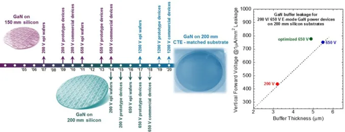
Initially, the development of GaN-based technology focused on high voltage (200 V and 650 V) power-switching applications. The first commercial 200 V e-mode GaN devices, fabricated on 150 mm Si substrates, were released in 2010 and the first 650 V commercial devices followed in 2014 (fig-ure 1, left). After first developing the technology on 100 mm [1, 2], and later 150 mm wafer sizes using Au-free metalli-zation schemes [3], imec has been pioneering 200 mm GaN-on-Si technology with first GaN 200 V epitaxy [4] and devices in 2014 [5–9]. The imec 200 mm GaN-on-Si e-mode transis-tor and diode platform was recently extended and qualified for 650 V applications. Today, the focus is on the technology development for higher level of integration and for 1200 V applications using 200 mm CTE-matched polycrystalline AlN substrates.
Current and future challenges. Because of the much higher CTE of GaN compared to Si, the GaN in-film stress during epi-taxial growth needs to be tuned compressive to compensate for the tensile stress during cool down. The use of 1.15 mm-thick 200 mm Si substrates is beneficial to reduce wafer warp during growth and hence avoiding wafer cracking. Without significant
hardware changes and lowering the robot speed of some handling systems, the thicker and heavier GaN-on-Si wafers can be processed in the standard imec CMOS fab. The warp specification of 50 µm is sufficiently low to avoid chucking
issues on electrostatic chucks. Prior to the fab introduction, the 200 mm GaN-on-Si wafers are tested for mechanical robust-ness, hereby reducing the wafer breakage during processing to less than 1%. After epitaxy, Ga and Al contamination on the wafer backside is unavoidable. Since Ga is a p-type dopant for Si, one of the major concerns of processing GaN wafers in a CMOS fab is Ga cross-contamination. The Ga and Al backside contamination after epitaxy is effectively removed by an in-house developed HF/H2O2-based cleaning procedure, hereby reducing the contamination level of the wafer backside and bevel to below 1011 at cm−2. Moreover, imec’s e-mode pGaN process flow contains (Al)GaN dry etch steps. A first step to dry etch the pGaN layer selectively to the AlGaN barrier layer, and a second to recess the AlGaN barrier in the ohmic contact areas. Since conventional F-containing cleaning recipes of the dry etch tools can form non-volatile GaFx species (i.e. GaFx is
not volatile below 800 °C), a Cl2-based clean that forms vola-tile GaCl3 at ~200 °C is used. This cleaning procedure effec-tively and reproducibly maintains the Ga contamination level in the dry etch tools well below the maximum allowed level.
Finally, since Au is a rapidly diffusing contaminant in Si that deteriorates the minority carrier lifetime, the GaN metal-lization schemes need to be Au-free. Because of the high bandgap and the absence of explicit doping of the epilayers, especially the development of Au-free ohmic contacts is chal-lenging. By using a Si/Ti/Al/Ti/TiN ohmic metal scheme and decreasing the alloy temperature to 565 °C, the ohmic con-tact resistance could be lowered to 0.3 Ω · mm with excellent reproducibility and uniformity.
Advances in science and technology to meet chal-lenges. Because the breakdown field of the Si substrate is ten times lower compared to GaN, the breakdown voltage of the power devices is dictated by the GaN buffer thickness. In figure 1 (right) the vertical buffer breakdown voltage (at 1 µA mm−2 leakage) is plotted versus the buffer thickness. Straightforward extension of the 3.2 µm-thick 200 V buffer
(red) to 5.5 µm for 650 V applications (blue) was resulting
in low wafer yield: the yield related to wafer breakage in the mechanical screening test was reduced from 90% for 200 V to 77% for 650 V. This issue was tackled by implementing Si substrates with high boron doping (0.01 Ω · cm resistiv-ity), hereby increasing the mechanical wafer strength, and by developing a new buffer concept with reduced thickness (4.9
µm, green) that resulted in an equally high buffer breakdown
voltage while maintaining the low buffer dispersion, and increasing the wafer yield for 200 V applications to 99% and to 97% for 650 V applications.
By optimization of the cleaning and dielectric deposition conditions, together with the field plate design, state-of-the-art 650 V 36 mm gatewidth power devices with 2.1 V thresh-old voltage (at maximum transconductance), 13 Ω · mm Ron
and 8 A output current (figures 2(a) and (b)) were obtained on 200 mm wafer size and processed in a standard CMOS wafer fab. Moreover, the devices exhibit dynamic Ron dispersion below 20% (10 µs on, 90 µs off) up to 650 V over the full
temperature range from 25 °C to 150 °C (figure 2(c)).
For 1200 V power applications, imec is working on using polycrystalline AlN (poly-AlN) substrates that have a better CTE-match to GaN. In this approach, a thin crystalline Si layer is transferred to a 200 mm poly-AlN substrate. This new technology is promising to go beyond the current technol-ogy limitations, because it is possible to grow thicker, higher quality GaN buffers on 200 mm substrates with a standard
Concluding remarks. GaN technology offers faster switch-ing power devices with higher breakdown voltage and lower on-resistance than Si, making it an ideal material for advanced power electronic components. For cost competitiveness, GaN power devices are preferably fabricated on large diameter Si substrates in existing Si CMOS fabs. Due to the large mismatch in lattice constant and thermal expansion coefficient, the epi-taxy of GaN on large diameter Si substrates is very challeng-ing. Imec has demonstrated for the first time that is possible to manufacture 200 V and 650 V GaN-on-Si e-mode devices in a 200 mm CMOS fab. For 1200 V applications, it is pro-posed to transfer the technology to 200 mm Si-on-poly-AlN
Figure 2. (a) Transfer and (b) output characteristics of a typical 36 mm gate width 650 V e-mode power device, and (c) the dynamic Ron
device dispersion. The devices were fabricated in imec’s 200 mm CMOS fab.
Figure 1. (Left) Timeline for 200 V, 650 V and 1200 V GaN-on-Si epi wafers, prototype and commercial enhancement-mode power
devices. (Right) Buffer leakage at 25 °C of imec’s 200 V (red) and 650 V (blue and green) GaN-on-Si epi wafers after full processing in the 200 mm CMOS fab.
2. Epitaxial lift-off of GaN and related materials for power device applications
P Fay1, J Wang1, L Guido2, J Xie3, E Beam3, R McCarthy4,
R Reddy4 and C Youtsey4
1 Department of Electrical Engineering, University of Notre Dame, Notre Dame, IN, United States of America
2 Virginia Tech; Department of Electrical and Computer Engineering, Materials Science and Engineering, Blacksburg, VA, United States of America
3 Qorvo, Inc., Richardson, TX, United States of America 4 MicroLink Devices, Inc., Niles, IL, United States of America
Status. GaN and other III-N compound semiconductors have had an enormous impact on optoelectronics—with the wide-spread adoption of LEDs, lasers, and solar-blind photodetec-tors—as well as RF electronics for both consumer wireless infrastructure and military communications and sensing. The continuing advance of III-N electronics promises to bring this revolution also into the power electronics space. With power device concepts based both on extensions of conventional lat-eral FET designs, as well as concepts based on vertical transis-tor designs, GaN and related materials promise to dramatically enhance the performance, efficiency, and ubiquity of sophisti-cated power management and control functions. Advances in growth and substrate technologies for achieving high-quality material, along with improved device designs, promise to enable continued increases in device performance. In addition, novel processing techniques are also promising to provide significant performance, cost, and integration improvements. Among these processing-related advances, techniques that enable epitaxial lift-off and substrate transfer are especially attractive. Epitaxial lift-off has been demonstrated for optoelec-tronic applications (see e.g. [11, 12]), and offers the potential for improved light extraction, a smaller device form factor, and ultimately more flexible displays as well as sensors for emerg-ing applications such as wearables. In the power application space, epitaxial lift-off can enable substantial increases in ther-mal performance (through improved heat removal), electrical performance (through lower resistive losses and higher break-down voltages), economics (through more efficient materials utilization, die size reduction, and substrate reclaim and reuse), and enhanced integrability with other electronics technologies. A range of epitaxial lift-off technologies for GaN and related materials have been demonstrated, including selective wet etching of ZnO layers [12], dry etching of epitaxial Nb2N lay-ers by XeF2 [13], mechanical exfoliation and separation using graphene or BN layers [14, 15], and band gap selective pho-toelectrochemical etching based on wet-chemical etching of lower-band gap materials such as InGaN [11, 16–18]. In addi-tion to the mechanism by which the lift-off occurs, epitaxial lift-off processes may be distinguished by whether they lift off a single device (figure 3(b)) or small circuit (e.g. [11, 13]), or seek to lift off a larger film (figure 3(a)) either for subsequent processing into devices (e.g. [12, 14, 15]) or after fabrication of the devices is largely complete (e.g. [17, 18]).
Current and future challenges. Advances in power electron-ics are poised to radically alter the design and implementation of electronic products and systems; ultimately, sophisticated power electronics and circuit topologies for enhanced effi-ciency and power-control capability could become ubiqui-tous if the key technological and economic challenges can be solved. Realization of this vision is currently constrained by cost, device performance, and integration challenges—all of which can be addressed by epitaxial lift-off. Due to the wide diversity of potential applications there is unlikely to be a single optimal solution; instead, we can expect different approaches to benefit different application segments. For example, for modest voltage and current requirements for which lateral devices (e.g. MISHEMTs) provide sufficient performance and economic benefit, use of conventional lattice-mismatched substrates such as SiC, sapphire, or Si is appropriate; epitaxial lift-off can then be used to accomplish substrate transfer for improved thermal or breakdown performance (see e.g. [19]), as well as the potential for reusing high-cost substrates (e.g. SiC) [13]. For applications where high currents and material-limited breakdown voltages are required, as well as applica-tions where economics dictates a high areal current density, vertical device structures offer inherent advantages. How-ever, these devices also place additional demands on material quality; while high dislocation densities are often tolerable in optoelectronic and lateral electronic nitride devices, these defects significantly compromise the performance of vertical devices. This can be addressed by homoepitaxial devices on
(a)
Figure 3. (a) Large-area (100 mm wafer) epitaxial lift-off of
GaN-based epitaxial device layers achieved using band-gap selective photoelectrochemical wet etching of an InGaN [17]; (b) single-die release of a GaN-based device using dry etching of Nb2N with XeF2 [13]. (a) [17] John Wiley & Sons. © 2017 WILEY-VCH Verlag GmbH & Co. KGaA, Weinheim.
bulk GaN substrates, but this in turn places more stringent demands on the epitaxial lift-off approach to avoid the genera-tion of dislocagenera-tions. The economic benefits of epitaxial lift-off from bulk GaN substrates are substantial, given their high cost and small diameter. In addition to substrate reuse, thermo-electric modelling indicates that direct bonding of lifted-off vertical FETs to a heatsink could enable die size reduction by more than 50% compared to devices on bulk GaN sub-strates [18]. Of the current techniques, only band gap selective photoelectrochemical etching with pseudomorphic InGaN release layers has been demonstrated to maintain fully
coher-Advances in science and technology to meet challenges. To address the challenges and fully realize the benefits of epitax-ial lift-off as an enabling technology for high-performance, low-cost, ubiquitous power electronics, significant techno-logical challenges must be overcome. For material-quality sensitive applications such as vertical devices, additional development of lattice-matched or pseudomorphic release layers is an important future direction. Current demonstra-tions have been based on the use of InGaN release lay-ers [11, 16–18]; while this approach has been successfully demonstrated for both single-die release and lift-off of large areas (>100 mm wafer), the lateral etch rate is modest and the surface morphology of the N-face GaN is not yet eas-ily controlled due to limited etch rate selectivity. Addition-ally, the use of pseudomorphic release layers such as InGaN have been reported to influence the mechanical behaviour of released structures [20]. Development of strain-control strat-egies or deposition of alternative release layer materials with basal plane lattices commensurate with the GaN devices are areas for future development and exploration. Another area that is largely unexplored to date is that of novel packag-ing and bondpackag-ing strategies to leverage the unique features of devices fabricated using epitaxial lift-off. The thermal per-formance of ultra-thin devices has been projected [18], but experimental validation and—in par ticular—optimization for the unique characteristics of ultra-thin devices is an area for additional development. Heterogeneous integration of lifted-off devices with conventional electronics, and packaging of lifted-off devices for emerging applications such as flexible or ultra-thin form factors is another area where substantial additional innovation is needed. Finally, the reliability of lifted-off devices is an important topic, but one that has not yet been addressed due to the nascence of the technology. Concluding remarks. Epitaxial lift-off is an emerging technology that is poised to be of significant benefit to the developing field of III-N based devices, and in particular to high-performance, cost-effective power electronics. The improvements in electrical and thermal performance, eco-nomic benefits derived from reduced die size and bulk GaN or SiC substrate reuse, and potential for enhanced heterogeneous integration with other electronics and packaging technologies makes epitaxial lift-off appear promising for advancing power (a)
(b) GaN
InGaN InGaN
GaN
Figure 4. (a) Measured current–voltage characteristics of typical GaN vertical PN junction diodes on prime bulk GaN substrate and on a reclaimed substrate (i.e. after growth, lift-off, repolish, and a second device growth and fabrication sequence, validating that device performance on epi-ready prime and reclaimed/reused substrates is nearly indistinguishable. (b) TEM image showing pseudomorphic InGaN release layer growth. [17] John Wiley & Sons. © 2017 WILEY-VCH Verlag GmbH & Co. KGaA, Weinheim.
3. GaN-on-Si 200 mm for power devices
L Di Cioccio, T Bouchet, M Charles, Y Baines, E Morvan, A Torres and M Plissonnier
CEA, LETI, L’Université Grenoble Alpes, Grenoble, France Status. The main objective in the LETI [21] power elec-tronic roadmap is the miniaturization of power converters to increase the energy efficiency of the systems while reduc-ing the cost. It is also important to improve reliability and ensure operation at higher temperatures (300 °C), with the markets of automotive (EV and HEV) and motor drives for industrial tools being targeted. To achieve these objectives for power convertors from a few watts to several hundred kW, it is essential to increase their operating frequency [22]. GaN-on-Si power devices are capable of responding to these requirements because GaN allows high frequency switch-ing (several MHz) and a higher power density than silicon (10 times greater), although these solutions must be imple-mented at the system level in order to fully benefit from the materials properties. Furthermore, GaN on 200 mm Si enables CMOS compatible technology leading to lower cost and improved robustness of the processes.
LETI has chosen to develop MOS Channel HEMT (MOSCHEMT) GaN architecture, fabricating ‘normally-off’ devices which give functionality similar to a classic silicon based MOS. To take full advantage of these devices, a route towards monolithic solutions for low and mid power applica-tions and a route towards system in package are promoted at LETI, figure 5, with five main axes of work: epitaxy, devices, passives, co-integration, and system architectures. Here, we will focus on the device roadmap.
Current and future challenges. Adoption of GaN in the industry requires high performance, high reliability devices produced at low cost. For automotive applications, GaN tran-sistors of 1200 V–50 A and 650 V–200 A are targeted. Current requirements are a RonS below 1 mohm · cm2, figure 6, with an Rdyn of no more than 10% of the RonS, meaning low losses [23]. The epitaxy is expected to improve in several ways: firstly, a constant improvement in the buffer layers and active layers to decrease the dislocation density, even though this has not been proven to be essential for high quality HEMT perfor-mance, and a reduction in point defects which cause trapping; secondly, a vertical leakage current lower than 1 µA mm−2 at 150 °C, and thirdly improvements and optimisations in the design of the epi stack, such as integration of back barriers to improve confinement of the free carriers in the potential well. Of course, all this has to be implemented while maintaining a wafer bow <50 µm for a silicon wafer thickness of 1 mm maximum to enable the process in standard 200 mm tools [24].
The most developed structure to make normally-off GaN HEMTs is pGaN gate architecture. P-type GaN may have a potential work function of up to 7.5 eV which makes pGaN, in a sense, an outstanding gate metal in addition to
the depolarization effect for depleting the channel beneath the gate. However, this design suffers from a compromise between the threshold voltage and the sheet resistance in the channel and so high positive threshold voltages are difficult to achieve. This is why at LETI we are developing an alterna-tive strategy, the MOSCHEMT. This architecture is a hybrid monolithic device which essentially puts a MOS channel and a HEMT drift layer in series. At the heart of this technology is the MOS gate, which needs to be reliable and robust; a chal-lenge that Si and SiC have already faced in the past.
Advances in science and technology to meet these challenges. The advances required to meet the challenges listed above can be described in five bullet points:
Simulation: to design complex architectures, capture process influence and describe device behaviour, simulations such as TCAD [25] are of major importance. Currently, significant efforts are needed to ensure simulators properly recreate the physics of III-N materials and devices.
Device characterisation: the JEDEC standards are not suffi-cient to fully qualify GaN-based power devices due to restric-tive criteria. Dynamic properties and aging effects, which show common patterns with dielectric aging, are key topics to be understood in order to bring GaN-on-Si products to indus-trial maturity in mass markets.
Device technology: as discussed above, constant improve-ments are required in the epitaxy, with in particular improved defect characterization and analysis of their impact on device performance. The understanding of the gate oxide trap pas-sivation will also be a significant scientific and technological challenge. The whole technology has to be CMOS compat-ible, which brings an additional constraint to GaN power device design, and the potential of GaN on 300 mm Si has to be investigated.
Thermal dissipation: the reduction in size of power devices when using GaN raises the challenge of thermal dissipation. In order to benefit from the full potential of GaN technology, the power density will need to be increased, and so process and packaging will need to be optimised to improve thermal dissipation.
Switching frequency: to allow high frequency switching, co-integration is key. Transistors, flyback diodes, rectifiers [26] or drivers [27] are examples of active devices that can be mon-olithically integrated to reduce parasitic elements and reach high performance converters.
Concluding remarks. The use of GaN-on-Si as a substrate for high power transistors is becoming an increasingly common choice, as an affordable large area alternative to expensive bulk substrates. Although there are still significant challenges to be overcome in order to produce high quality devices on these substrates, GaN devices will take full advantage of both the remarkable properties of GaN, and of production in
CMOS compatible fabrication plants to achieve high perfor- and encourage the use of this technology. With all of these
Figure 5. Power systems roadmap at LETI. An SOC (system on chip) route towards monolithic solutions is important for miniaturization
for low and mid power solutions. For higher voltages, an ultra-compact power module is preferred [21].
Figure 6. Specific on resistance versus breakdown voltage. Benchmark of different laboratory results versus CMOS or non CMOS
4. Buffer design in GaN-on-Si power devices
Michael J Uren1, David J Wallis2,3 and Martin Kuball1
1 Centre for Device Thermography and Reliability, University of Bristol, United Kingdom
2 Cambridge Centre for GaN, University of Cambridge, United Kingdom
3 Centre for High Frequency Engineering, University of Cardiff, United Kingdom
Status. Uptake of GaN devices for power applications requires that they can be manufactured in volume at compa-rable cost to Si components, and with validated device reli-ability. The key innovation that has made this possible is the ability to grow epitaxial device quality layers of GaN and AlGaN on 6″ or 8″ (1 1 1) Si wafers. Together with the devel-opment of Si CMOS compatible device process flows, this has allowed GaN power devices to be fabricated using existing Si fabrication lines with Si and GaN processing occurring in par-allel. This section addresses the electrical and material design of the GaN-on-Si epitaxial platform that is now being used to realise HEMT devices for power applications.
GaN HEMTs were first successfully grown on Si in the 1990s, however the epitaxy did not have sufficient break-down voltage for power applications. GaN-on-SiC RF devices used Fe doping to suppress short-channel drain leakage and increase drain breakdown, representing the first realiza-tion that the nominally insulating GaN layer underneath the 2DEG channel is actually electrically active and needs just as much design and optimisation as the upper barrier and chan-nel region. However, Fe doping was found to deliver insuffi-cient breakdown voltage when applied to high voltage power devices. Eventually, it was found that a combination of a com-plex strain relief buffer together with carbon doping to con-trol breakdown could achieve sufficient voltage handling [28]. Unfortunately, there continued to be bulk trapping related issues collectively known as dynamic RON dispersion or cur-rent collapse, and their solution has only recently been dem-onstrated commercially. The reasons for the wide variation in dynamic RON performance achieved for apparently identical carbon doped epitaxies are only now becoming understood. Current and future challenges. Key issues in epitaxial growth of GaN-on-Si are the lattice and thermal expansion coeffi-cient mismatches which make strain management critical. As a result, large numbers of defects (>1010 cm−2) are gener-ated, and cracking of the GaN layers can occur on cooling from the growth temperatures (≈1000 °C) [29]. The epitaxial layer structure which has been adopted to solve these issues is shown in figure 7. A nucleation layer of AlN is universally used to initiate growth and avoid the Ga/Si eutectic that causes ‘melt-back’. This is followed by a strain relief stack, where two successful approaches have been found based on either a step-graded AlGaN layer [30], or a superlattice of AlN/GaN [31]. The detailed stack design is normally proprietary. These buffers are used to induce compressive strain during growth which counteracts the tensile strain introduced on cooling,
preventing cracking and yielding a flat wafer. To aid growth uniformity, thick Si substrates (1 mm) tend to be adopted, which also helps to reduce the wafer breakage during process-ing which has been observed for standard thickness wafers (675 µm). Total epi-layer thickness as large as 8 µm can be
achieved, but the challenges of wafer bow and stress become more difficult to overcome. Typical dislocation densities at the surface of the stack, i.e. at the 2DEG, are ≈109 cm−2.
Due to the incorporation of impurities and point defects, as-grown GaN is typically n-type and it has been found that it is essential to add deep level dopants to suppress leakage. The dopant of choice is carbon [28] with a density well above 1018 cm−3 delivering excellent isolation and breakdown voltage. Carbon primarily incorporates substitutionally on the nitro-gen site [32]. This pins the Fermi level about 0.9 eV above the valence band making the GaN:C p-type, with electrical transport being via low mobility holes rather than electrons. It is found that the carbon doping must be spaced away from the active 2DEG to reduce trapping effects [33]. A key issue with carbon doping is current collapse (dynamic RON) [34]. Charge trapping occurs in the epitaxial bulk during off-state operation when there is high drain bias. When the device is switched on, trapped negative charge reduces the electron density in the active channel and increases the on-resistance. Some current commercial devices show as much as a factor of two increase following off-state bias.
Advances in science and technology to meet chal-lenges. Suppression of current collapse is key for technol-ogy uptake. The p-type nature of GaN:C means that there is a p-n junction between the 2DEG channel and the bulk of the epitaxy, meaning that the bulk can be electrically floating. Suppression requires that this floating buffer is grounded to the active 2DEG channel preventing it from providing a back bias, and hence, counter-intuitively, a vertical leakage path is essential. Figure 8 shows an electrical network representation of the buffer, and simulations to show the impact of differ-ent leakage paths [35]. It is found that there is a trade-off between vertical leakage and current-collapse, with careful process control of leakage paths being absolutely required. Current state-of-the-art power devices are able to achieve less than 10% change in RON in the 25 °C–150 °C temperature range by careful leakage control [36]. Recently it has been shown that changing the stoichiometry of the Si3N4 surface passivation can change the bulk vertical leakage and con-trol the dynamic RON [37]. Further work is still required to achieve a guaranteed simultaneous optimisation of leakage and current collapse.
Many power switching topologies require the series con-nection of devices. Current technologies would require a hybrid packaging approach to prevent an undesirable Si substrate bias being applied to the upper transistor in a half-bridge configuration. New approaches to allow transistor elec-trical isolation are therefore required before full integration is feasible. One approach being investigated is the use of buried oxide layers with 200 V isolation being achieved by imec.
Operating at voltages much above 650 V will require the growth of thicker epitaxy, and that requires a solution to
reducing stress. Although single crystal GaN or AlN would be the ideal substrates, cost and wafer size make this unlikely to have any impact. One possible approach is the use of thermal expansion matched substrates as an alternative to Si wafers. For example, polycrystalline AlN wafers have been successfully used as a growth substrate, achieving 18 µm thick epitaxial
layers.
Concluding remarks. GaN-on-Si based power transistors are already achieving impressive performance and reliability based on the remarkable ability to grow strain-engineered, electrically-optimised, high-quality epitaxy on low cost 6″ or 8″ Si wafers. Buffer-related trapping leading to dynamic RON has been a serious issue, requiring a delicate balance between leakage and performance for its suppression. This is only now being achieved by commercial suppliers. Going significantly beyond the current 650 V market segment to much higher voltages will require major changes and innovation in the substrates and epitaxy to allow thicker epitaxial layers to be grown yet still retaining control of wafer bow.
Acknowledgments
This work was funded by the UK EPSRC PowerGaN project K0114471/1.
(a)
(b)
Figure 8. (a) Schematic showing leakage and capacitive paths within
the buffer. ① to ④ indicate some of the key locations where charge accumulates. (b) Simulated dynamic RON for different leakage paths within the buffer. All these different behaviours are observed in practice. © 2017 IEEE. Reprinted, with permission from [35].
Figure 7. (a) Schematic cross-section of the typical epitaxial layer structure used for the manufacture of GaN-on-Si HEMTs. (b) TEM
5. Challenges in growth for GaN power electronics
Joseph J Freedsman1 and Takashi Egawa1,2
1 Research Center for Nano-Devices and Advanced Materials, Nagoya Institute of Technology, Nagoya 466 8555, Japan 2Innovation Center for Multi-Business of Nitride Semiconductors, Nagoya Institute of Technology, Nagoya 466 8555, Japan
Status. GaN based devices are promising for many power applications such as switching functions and inverters that can save a significant amount of energy. The performance and efficiency of these GaN power devices greatly rely on the epitaxial growth of GaN and related alloys. High quality GaN epitaxial growth can be achieved by using native free-standing GaN substrates. However, the downside of epitaxial GaN-on-GaN is it is expensive and only small-diameter GaN substrates. This in turn impede the mass production of GaN power devices at an affordable cost for commercial applica-tions. To overcome this, the heteroepitaxial growth of GaN is carried out on foreign substrates such as silicon carbide (SiC), sapphire and silicon (Si). From commercial aspects, the heteroepitaxial growth of GaN-on-Si is attractive because of the large-size scalability of inexpensive Si substrates. Nev-ertheless, the areas of concern are the large differences in the physical properties between wide bandgap GaN and Si sub-strate that often results in poor crystal quality leading to high dislocation density, pits and cracks for GaN-on-Si. Therefore, appropriate epitaxial growth of GaN-on-Si and subsequent fabrication processes are absolutely necessary for power device applications. For example, several switching applica-tions require lateral GaN-on-Si high-electron-mobility tran-sistors (HEMTs) with high breakdown voltage (BV) [38]. To realize these GaN-on-Si lateral devices, we have used the met-alorganic chemical vapor deposition (MOCVD) grown thick-AlN initial layer and GaN/thick-AlN strained layer superlattice (SLS) structures. The AlGaN/GaN HEMTs grown on 8-inch silicon by using similar epitaxial growth technique delivered a high BV of 1.6 kV. For expanding the applications to electric and hybrid vehicles, high performance GaN power devices are required to drive high-power motors, power modules such as DC-DC converter and inverters. Typically, in these applica-tions high-voltage GaN-on-Si vertical devices with reduced chip area are preferred. To facilitate the fabrication process of such devices, we have successfully grown thick GaN-on-Si vertical structures by using conductive buffer layers compris-ing of thin-AlN initial layer and SLS. The recent advances in the hetero epitaxial GaN-on-Si are encouraging for the growth of GaN power electronics on larger diameter Si substrates. Current and future challenges. Despite their merits, GaN-on-Si power devices have also associated technical challenges which need attention. Of these, the most important issue is the growth of a high-quality and thick GaN-on-Si. The large differences in lattice constants and thermal expansion coef-ficient between GaN and Si are responsible for the difficulties
in the growth of high-quality and thick GaN-on-Si. The inset of figure 9 shows the cross-sectional structure of AlGaN/GaN HEMT on Si using metalorganic chemical vapour deposition (MOCVD). High temperature growth of GaN-on-Si could likely result in melt-back etching of Si substrate caused by Ga atoms [39]. As a result, deep pits, dislocations and cracks could arise, which in turn would deteriorate the device perfor-mance like an increase in buffer leakage, and reduced break-down [40]. Therefore, the growth of high-temperature-grown AlN nucleation layer (NL) is indispensable to avoid both the melt-back etching and deep pits. Recent studies have revealed the influence of AlN NL on the vertical breakdown charac-teristics for GaN-on-Si and the AlN NL with better surface morphology and lower O impurity were preferred to grow highly resistive buffers [41]. Figure 9 illustrates the typical relationship between wafer bowing and total epitaxial thick-ness for the AlGaN/GaN HEMT on 4-inch Si. From this cor-relation, it could be understood that the use of GaN/AlN SLS is effective in controlling the bowing [42]. Subsequently, the growth of SLS is essential to control the wafer bowing for GaN-on-Si. Additionally, thick epi layers grown by using SLS multipairs supressed the vertical leakage and showed a verti-cal breakdown field of 2.3 MV cm−1 [43]. A high lateral BV
Off of 1.4 kV was also demonstrated for AlGaN/GaN HEMT on Si grown with the above recommendations [44]. The recent systematic investigations and the promising results as dis-cussed earlier would provide substantial understanding for the growth dynamics of epitaxial GaN typically on 8-inch Si substrates. Indeed, our AlGaN/GaN HEMT on 8-inch Si has shown a three-terminal off-state breakdown voltage 1650 V for the gate–drain distance of 50 µm. The availability of mod-ern MOCVD reactors with multi-wafer capability and evalu-ation tools suggest promising features for GaN-on-Si lateral power devices. 1.25 µm 0 120 0 1.0 2.0 3.0 4.0 5.0 6.0 Wafe r bo wi ng (µ m) 7.0 150 90 60 30 4.0 µm Thickness of GaN/AlN SLS: 5.0 µm 2.5 µm
Thickness of epitaxial layer (µm)
8.0 Si(111) Sub. HT-AlGaN/AlN AlGaN GaN/AlN SLS GaN : Full structure
: Sample without AlGaN/GaN
Figure 9. Wafer bowing as a function of total epitaxial layer thickness of AlGaN/GaN HEMT on Si. © 2012 IEEE. Reprinted, with permission, from [42].
Advances in science and technology to meet chal-lenges. GaN-on-GaN vertical devices are expected to play a vital role in future high-power conversion applications as it can reduce the overall chip area. However, GaN substrates have disadvantages such as limited wafer size and being expensive. Therefore, the realization of GaN-on-Si vertical devices is the upcoming challenge owing to growth and fab-rication difficulties. Unlike the lateral AlGaN/GaN devices, a deeper understanding on the growth and fabrication of GaN-on-Si vertical devices is required for potential power device applications. Some researchers have demonstrated GaN-on-Si vertical p-n diodes fabricated by wafer bonding and substrate removal technology [45]. This technique could complicate the fabrication process and eventually lead to increase in cost. Others showed GaN p-n diodes by using a quasi-vertical structure [46]. Irrespective of these methods, a detailed study is required for the growth of GaN-on-Si verti-cal structures that should complement the fabrication as well. To realize such a GaN-on-Si vertical device, (i) the doping density (Nd-Na) in the drift region must be controlled and (ii) the buffer layer should be conductive. Figure 10 represents
the net Nd-Na in the drift region as a function of SiH4 flow rate for a GaN-on-Si grown with two SLS thicknesses. As shown, the Nd-Na could be controlled for GaN-on-Si by increasing the SLS multipairs, which is due to the reduction of dislocation density. The conductive buffer layers including the AlGaN/ AlN layers and SLS are indispensable for realizing GaN-on-Si vertical devices. Therefore, a GaN-on-Si-doped AlN NL as thin as 3 nm was initially deposited followed by the deposition of Si-doped AlGaN and SLS. This novel fully vertical GaN-on-Si p-n diode comprises of doped buffer layers and not involve substrate removal technology. This GaN-on-Si p-n diode has ohmic contacts on the p-GaN layer and a backside of n + -Si substrate that showed a turn-on voltage of 3.4 V and a break-down voltage of 288 V for the 1.5 µm-thick n−-GaN drift layer [47]. The BV can be further improved by increasing the buffer thickness and/or by using field plate structures. These improvements in the MOCVD growth of GaN-on-Si vertical structures suggest their potential role in power electronics in near future.
Concluding remarks. GaN-on-Si power devices are emerging to play a dominant role in the next-generation power electron-ics. Significant improvements in the hetero epitaxial growth and device fabrication are indispensable for the commercial-ization of these power devices. For the epitaxial growth of GaN-on-Si lateral devices, we have utilized the high temper-ature AlN NL to prevent the melt back etching of Ga into Si. It was also found that the growth of SLS is essential to control the wafer bowing for GaN-on-Si. In addition, the growth of SLS multipairs effectively enhanced the breakdown volt age of on-Si HEMTs. On the other hand, fully-vertical GaN-on-Si p-n diodes were demonstrated by using conductive buf-fer layers. We have used AlN NL as thin as 3 nm and SLS multipairs, both highly doped in order to realize fully-vertical GaN-on-Si p-n diodes. These advancements in the MOCVD growth of GaN-on-Si and device fabrication processes will lead to the high-performance power electronics.
Acknowledgment
The authors would like to thank the Super Cluster Program of the Japan Science and Technology Agency.
Nd -Na
(c
m
-3 )
SiH4flow rate (sccm) 2.3 µm-thick GaN/Sapphire SD=1.4×108cm-2 ED=2.0×109cm-2 GaN/Si (Sample A) SD=1.5×109cm-2 ED=8.8×109cm-2 GaN/Si (Sample B) SD=1.4×109cm-2 ED=3.5×1010cm-2 1015 1016 1017 1018 1019 0.1 1.0 10 GaN/AlN SLS 3 µm n-GaN: 1 µm n+-Si(111) AlGaN/AlN Sample A n+-Si(111) AlGaN/AlN GaN/AlN SLS 0.5 µm n-GaN: 1 µm Sample B
Figure 10. Net doping concentration as a function of SiH4 flow rate for GaN-on-Si with different SLS thickness. For comparison, the data of GaN/sapphire are also shown. Reproduced from [47]. © 2016 The Japan Society of Applied Physics. All rights reserved.
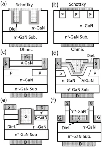
6. Vertical GaN power devices
Yuhao Zhang, Jie Hu, Min Sun, Daniel Piedra, Nadim Chowdhury and Tomás Palacios
Department of Electrical Engineering and Computer Science, Massachusetts Institute of Technology, Cambridge, MA, United States of America
Status. Central to improving the efficiency of power electron-ics is the availability of low-cost, efficient and reliable power switching devices. GaN-based devices are exciting candidates for next-generation power electronics. Currently, both lateral and vertical structures are considered for GaN power devices. Vertical GaN power devices have attracted significant atten-tion recently, due to the capability of achieving high break-down voltage (BV) and current levels without enlarging the chip size, the superior reliability gained by moving the peak electric field away from the surface into bulk devices, and the easier thermal management than lateral devices [48].
Since 2010, the field of vertical GaN power devices has grown exponentially and seen numerous demonstrations of vertical diodes and transistors (figure 11). A 3.7 kV vertical GaN pn diode [49] and a 1.1 kV vertical GaN Schottky bar-rier diode (SBD) [50] have recently showed near-theoretical power figure of merit. Trench metal-insulator-semiconductor barrier Schottky diodes [51] (figure 12(a)) and junction barrier Schottky diodes [52] (figure 12(b)) have also been proposed to combine the good forward characteristics of SBDs (e.g. low turn-on voltage) and reverse characteristics of pn diodes (e.g. low leakage current and high BV).
Several structures have been proposed for vertical GaN transistors, with the highest BV close to 2 kV. Current aperture vertical electron transistor (CAVET) combines the high con-ductivity of a two-dimensional electron gas (2DEG) channel at the AlGaN/GaN heterojunction and the improved field distri-bution of a vertical structure [53] (figure 12(c)). The CAVET is intrinsically normally-on, but a trench semi-polar gate could allow for normally-off operation [54] (figure 12(d)). Vertical GaN trench MOSFETs have no 2DEG channels, but do not need the regrowth of AlGaN/GaN structures and are intrinsi-cally normally-off [55] (figure 12(e)). Recently, vertical fin MOSFETs have been demonstrated to achieve normally-off operation without the need for p-type GaN materials or epi-taxial regrowth [56] (figure 12(f)).
While most vertical devices utilize expensive GaN sub-strates, it is also feasible to make vertical GaN devices on low-cost Si substrates. Quasi- and fully-vertical GaN-on-Si vertical diodes have been demonstrated with a BV over 500 V and excellent high-temperature performance [46]. These devices can enable 100-fold lower substrate and epitaxial cost than GaN-on-GaN vertical devices.
Current and future challenges. In spite of the great progress, the full potential of vertical GaN SBDs and transistors has not been exploited yet. The BV demonstrated in these devices, with no avalanche capability reported, is still much lower than the avalanche BV in vertical GaN pn diodes. The lack
of avalanche capability would greatly compromise the device robustness when operating in inductive switching environ-ments. Although the nature of avalanche breakdown is still not fully understood in GaN devices, a key factor is believed to be good edge termination technologies and a way to remove holes from the structure. In SiC power devices, successful edge termination technologies, such as junction termination extension and field rings, was enabled by selective p-type ing. However, in GaN devices, the current selective area dop-ing or selective area epitaxial regrowth technologies cannot yield material of sufficiently high quality to enable defect-free patterned lateral pn diodes. In particular, p-type implantation and activation in GaN is far from mature. With complicated activation annealing schemes, the activation ratio for accep-tors is typically below 5%, resulting in very low concentration and mobility for the activated free holes [52].
There remain some open questions on the selection of car-rier channels in vertical GaN transistors to improve the device forward characteristics. The ideal channel for these devices would have normally-off configuration with high carrier mobil-ity and without the need for epitaxial re-growth. Further work is needed for all the three channels reported so far, 2DEG channel [53], MOS inversion layer [55] and bulk fin channel [56].
The commercialization of vertical GaN power devices has been hindered by the high cost of bulk GaN substrates. The mainstream GaN substrates are 2-inch, while 4- and 6-inch GaN substrates are available very recently in small vol-umes. The wafer cost (per area) for 2-inch GaN-on-GaN is $60–$100/cm2, still much higher than the cost for 4-inch SiC (~$8/cm2) and 8-inch GaN-on-Si (~$1/cm2). The fundamen-tal challenge is how to achieve the material quality associated with free-standing GaN substrates, while allowing the devices to be transferred to alternate substrates and have the GaN sub-strates re-used to reduce cost.
Advances in science and technology to meet chal-lenges. Different technological solutions can be envisioned to address the challenges in making patterned lateral pn junc-tions for edge termination structures. For example, compared to p-type ion implantation, n-type ion implantation (e.g. Si, N, etc) and activation is much easier. Lightly-doped p-GaN edge
Figure 11. Overview of the main device types and voltage classes
terminations has been then demonstrated by implanting donors to compensate highly-doped p-GaN layers in vertical GaN pn diodes [49]. Patterned pn junctions have also been reported by n-type ion implantation into epitaxially grown p-GaN regions [52]. Besides selective ion implantation, patterned pn junc-tions can be also made by selective p-GaN regrowth to fill n-GaN trenches. The initial feasibility of this approach has
been demonstrated in CAVET [53], although much more work is needed to study the regrown interface quality and passivate parasitic leakage currents.
In parallel, different electrical, mechanical and chemi-cal techniques are under development to enable devices to be lifted off from native GaN substrates and transferred to low-cost substrates. Successful layer transfer technology, combined with patterned interconnections on the supporting substrate and re-use of GaN substrates, should greatly reduce the cost and pave the way to commercialize high-performance vertical GaN power devices.
Another approach that can fundamentally circumvent the cost issue of vertical GaN devices is to fabricate them on Si substrates, which could allow for almost 100-fold lower wafer and epitaxial cost as well as 8-inch fabrication. Recently, GaN-on-Si vertical pn diodes with blocking capability of 500–600 V have been demonstrated [46]. Fully-vertical GaN-on-Si power devices have also been demonstrated by differ-ent technologies, such as layer transfer, conductive buffer layer, and selective removal of the substrate and buffer layer. To improve the performance of these devices, advances in epitaxial growth technology are needed to enable thicker GaN layers with very low background carrier concentration (<1016 cm−3) on Si substrate.
Concluding remarks. Vertical GaN devices are key to achieve the high currents (>100 A) and voltages (>600 V) required by many power applications, such as electric vehicles and renewable energy processing. Record performance near the theoretical Baliga figure of merit has been demonstrated in vertical GaN pn diodes, although more work is needed in ver-tical Schottky barrier diodes and transistors. Exciting research opportunities exist in the field, especially in making patterned pn junctions, recycling GaN substrates and developing verti-cal GaN devices on Si substrates.
Acknowledgments
The authors gratefully acknowledge the funding support by the ARPA-E SWITCHES program monitored by Dr T Heidel and Dr I Kizilyalli, and by the ONR PECASE program moni-tored by Dr Paul Maki.
Figure 12. Schematic of representative vertical GaN advanced
Schottky barrier diodes and vertical GaN transistors: (a) trench MIS barrier Schottky diode, (b) junction barrier Schottky diode, (c) CAVET, (d) trench CAVET, (e) trench MOSFET and (f) vertical fin MOSFET. In this figure, ‘Diel.’ stands for dielectrics, and ‘Sub.’ for substrates.
7. GaN insulated gate field-effect transistors
Kevin J Chen1, Mengyuan Hua1 and Shu Yang2
1 The Hong Kong University of Science and Technology, Hong Kong, People’s Republic of China
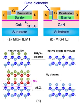
2 Zhejiang University, Hangzhou, People’s Republic of China Status. GaN-based insulated gate field-effect transistors with an insulating gate dielectric provide many desirable proper-ties such as suppressed gate leakage and large gate voltage swing [57]. These devices are typically in the form of metal-insulator-semiconductor HEMT (MIS-HEMT) or MIS-FET with the insulating dielectric on a heterojunction (e.g. AlGaN/ GaN) channel or a GaN channel, respectively, as illustrated in figures 13(a) and (b). The MIS-HEMT was first studied for RF/microwave power amplifier applications [58], and then intensively investigated as a promising power switching device. The MIS-gate transistors are especially attractive to high-frequency power switching applications because they can better tolerate gate voltage over-shoot that often occurs in circuits with high slew rate.
As is the case of Si- and SiC-based MOSFETs, the gate dielectric in GaN insulated gate FETs is required to deliver a dielectric/III-nitride interface with low trap density, high reliability and long lifetime under various stresses (e.g. elec-trical, thermal, humidity, etc). GaN MIS-HEMTs typically exhibit depletion-mode (D-mode) operation with a large nega-tive threshold voltage (Vth) because of the presence of high-density positive polarization charges in the barrier layer (e.g. AlGaN). The D-mode MIS-HEMT, with its gate (input) termi-nal seldom forward biased during circuit operation, typically exhibits less adverse effects from the gate dielectric. This is mainly due to the presence of the barrier layer that decou-ples the 2DEG channel from the interface/border traps in the dielectric as long as the ‘spill-over’ of electrons toward the dielectric does not occur, leading to small Vth hysteresis. Very good gate reliability [59] has been obtained in D-mode MIS-HEMTs featuring a thin gate dielectric layer (SiO2, Si3N4 or high-κ dielectrics) under relatively small forward gate bias.
Enhancement-mode (E-mode) HEMTs and MIS-FETs with a positive Vth are highly desirable from the cir-cuit application point of view for their simpler gate control circuitry and fail-safe operation. To fully turn on the chan-nel current, however, large positive forward gate needs to be applied. This is when the gate dielectric is under the most demanding operational conditions (e.g. high electric field, charge injection to the dielectric and carriers leaking through the dielectric). Vth-instability (both static and dynamic) at dif-ferent temperatures and bias stress conditions, and its impact on dynamic on-resistance (RON), needs to be systematically studied and clearly understood [60, 61]. The time-dependent dielectric breakdown (TDDB) is the ultimate hurdle to over-come before commercialization of E-mode GaN-based MIS-HEMTs and MIS-FETs.
Current and future challenges. Trap states at the di electric/ III-nitride interface and inside the dielectric present the
biggest challenges to GaN MIS-HEMTs and MIS-FETs [62]. With a wide bandgap in GaN, a large energy window is avail-able to accommodate interface and bulk trap states at shal-low and deep energy levels with short and long emission time constant τit. The dynamic charging/discharging processes of these traps could lead to VTH instability during a switching operation, and consequently affect circuit and system stability.
Unlike Si on which highly uniform and highly reli-able thermal oxide can be prepared using high-temperature (800 °C–1200 °C) furnaces, GaN surface becomes unstable when the ambient temperature exceeds 800 °C. In addition, the Ga–O bonds at an oxide/III-nitride interface fundamentally induce high-density gap states, except in a few very specific crystalline oxide configurations, according to a first-principles calculation study [63]. Thus, removing the detrimental Ga–O bonds at the GaN surface is a critical step for obtaining low interface trap density (Dit). If oxide-based gate dielectric is to be used for their high dielectric constant and large band-gap, a non-oxide (e.g. nitride-based) interfacial layer would be highly desirable.
Although there are many reports on E-mode GaN MIS-HEMTs and MIS-FETs in research literature, the commer-cialization of these devices has been hindered by concerns over the gate dielectric reliability. The commonly used gate di electric (SiN, SiO2 and Al2O3) is deposited by PECVD or ALD (atomic layer deposition) at relatively low temper-ature (at 300 °C–400 °C). While the low temperature helps maintain GaN surface morphology, it is also the main reason for high-density defects in the dielectric, making it difficult for these devices to pass reliability tests and qualifications. High-temperature annealing only shows a moderate effect
Figure 13. Schematic cross sections of GaN-based (a) MIS-HEMT
and (b) MIS-FET. (c) Schematic process for in situ native oxide removal and surface nitridation of GaN.
on enhancing the dielectric reliability. Thus, it is of critical importance to develop high-temperature gate dielectric films (e.g.~ 800 °C or above) with lower defect density and longer TDDB lifetime. The biggest challenge to high-temperature dielectric on GaN is the degradation (via decomposition or chemical reaction) of GaN surface at high temperatures. A possible solution could feature a low-temperature interface protection layer and high-temperature gate dielectric.
Advances in science and technology to meet challenges. The first D-mode GaN MIS-HEMT was demonstrated using
MIS-HEMTs and fully MIS-FETs have both been developed with low on-resistance, high saturation current, small Vth hys-teresis and low dynamic on-resistance. In particular, in situ removal of native oxide and consequent nitridation by low-power plasma (as illustrated in figure 13(c)) prior to dielectric deposition [65] are important techniques for producing high-quality dielectric/GaN interface by passivating the dangling bonds while introducing minimum gap states.
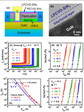
To achieve high gate dielectric reliability under large posi-tive gate bias required for E-mode insulated gate FETs, SiNx
deposited by LPCVD (low-pressure chemical vapor deposi-tion) has emerged as a compelling candidate as it possesses several important benefits including large conduction band offset with GaN (ΔEc ~ 2.3 eV), relatively high dielectric constant (κ ~ 7) and especially the long TDDB lifetime as
a result of the low defect density achieved at high deposition temper ature (e.g. 780 °C). Implementing the LPCVD-SiNx
gate di electric in recessed-gate E-mode MIS-HEMTs and MIS-FETs has been more challenging since an etched GaN surface suffers more severe degradation than an as-grown GaN surface at high temperatures. An effective approach to suppress such a degradation while maintaining low Dit (1011–1012 cm−2 eV−1) has been developed using a low-temper ature PECVD-SiNx thin film as an interfacial
protec-tion layer [66], as depicted in figure 14. For a 10-year lifetime, the maximum gate bias is determined to be 11 V at a failure rate of 63.2% and 9.1 V at a failure rate of 0.01%.
Concluding remarks. There is strong demand for GaN insu-lated gate field-effect transistors with both depletion- and enhancement-mode operations, as the insulated gate provides strong immunity to control voltage spikes and could be driven with circuits very similar to those used for the mainstream Si and SiC power MOSFETs. The most critical need of a GaN insulated gate FET technology is a gate dielectric technique that simultaneously delivers low interface/bulk trap density and robust reliability under stringent electrical and thermal stresses. The E-mode GaN MIS-HEMTs and MIS-FETs are especially challenging as they operate under large positive gate bias and the recessed-etched GaN demands better protec-tions during high temperature processes associated with high-quality dielectric deposition. Combining low-temperature interfacial layer with high-temperature gate dielectric could be a promising pathway toward reliable and stable GaN
insu-Figure 14. (a) Schmematic cross section of an E-mode fully
recessed GaN MIS-FET with interfacial protection layer. (b) High-resolution TEM of an LPCVD-SiNx/PECVD-SiNx/GaN interface. (c) Time to breakdown (tBD) of the LPCVD-SiNx MIS-FETs with interfacial protection layer at forward gate stress of 18, 17, 16 and 15 V at 25 °C. (d) Weibull plot of the electric field-dependent tBD distribution. (e) Lifetime prediction with a failure rate of 63.2% and 0.01%, respectively. (f) Weibull plot of the temperature-dependent
![Figure 3. (a) Large-area (100 mm wafer) epitaxial lift-off of GaN- GaN-based epitaxial device layers achieved using band-gap selective photoelectrochemical wet etching of an InGaN [17]; (b) single-die release of a GaN-based device using dry etching of](https://thumb-eu.123doks.com/thumbv2/123doknet/13794809.440742/8.892.504.798.83.513/figure-epitaxial-epitaxial-achieved-selective-photoelectrochemical-etching-release.webp)