ACCURACY OF NOISE MEASUREMENTS
by
Judith Ann Furlong Submitted to the
DEPARTMENT OF ELECTRICAL ENGINEERING AND COMPUTER SCIENCE In partial fulfillment of the requirements
for the degrees of BACHELOR OF SCIENCE
and
MASTER OF SCIENCE at the
MASSACHUSETTS INSTITUTE OF TECHNOLOGY
June, 1990
®Judith A. Furlong
The author hereby grants to MIT permission to reproduce and to
distribute copies of this thesis document
in whole or in part.
Signature of Author
"Department of Electrical Eineering and Computer Science, May 11, 1990
Certified by
Hermann A. Haus, Thesis Supervisor
Certified by
SumnerBro'p Company Supervisor
Accepted by
Arthur
'.Smith,
Chair,
Department Committee on Graduate StudentsMASSACHUSETS INSTITUTE
OF TECHNOLOGY
ACCURACY OF NOISE MEASUREMENTS by
Judith Ann Furlong
Submitted to the Department of Electrical Engineering and Computer Science on May 11, 1990 in partial fulfillment of the requirements for the Degrees of
Master of Science and Bachelor of Science in Electrical Engineering
ABSTRACT
Two systems that measure the white noise spectrum of voltage reference diodes, in the frequency range from 1 kHz to 100 kHz, were analyzed to determine their accuracy. Limitations to the accuracy of each of these system were identified. Recommendations were make for improving the accuracy of these existing systems.
The results of the analysis on these systems show that the system, which used the HP 3562A Dynamic Signal Analyzer to measure noise, had an accuracy of one-half percent. The other system, which used the Fluke 8506A Thermal RMS Multimeter to measure noise, was expected to have the same, if not slightly better, accuracy.
Thesis Supervisor: Prof. Hermann Haus
ACKNOWLEDGEMENTS
I would like to thank my thesis advisers, Sumner Brown and Prof. Haus for their insight, support and patience. I would especially like to thank Randy Pflueger for getting me involved in this project and for his help over the past three years. Thanks also to the members of 15G/EBD for there advice and support during my stay at CSDL. Finally I would like to express my gratitude to my mother, Helen Furlong, for her love and encouragement.
This report was prepared at the Charles Stark Draper Laboratory, Inc. under Contract F04704-86-C-0160.
Publication of this report does not constitute approval by the Draper Laboratory or the sponsoring agency of the findings or conclu-sions contained hearin. It is published for the exchange and stimula-tion of ideas.
I hereby assign my copyright of this thesis to The Charles Stark Draper Laboratory, Inc., Cambridge, Massachusetts.
Judith A. Furlong
Permission is hereby granted by The Charles Stark Draper Laboratory, Inc. to the Massachusetts Institute of Technology to reproduce any or all of this thesis.
TABLE OF CONTENTS Abstract Acknowledgements List of Illustrations Section 1 Section 2 INTRODUCTION 1.1 Introduction 1.2 Organization of Thesis BACKGROUND
2.1 Tunneling and Avalanche Breakdown 2.2 Limitations of Noise Measurements 2.3 Methods of Measuring Noise
2.3.1 Sine Wave Method of Noise Measurement 2.3.2 Noise Generator Method of Noise
Measurement
2.3.3 Correlation Method of Noise Measurement 2.4 Typical versus State-of-the-Art Noise
Measurements
2.5 Lukaszek's Noise Measurements
2.5.1 Lukaszek's Noise Measurement System 2.5.2 Measurement Procedure
2.5.3 Noise Ratio
Section 3 DESCRIPTION OF THE NOISE MEASUREMENT SYSTEMS 3.1 The First Measurement System
3.1.1 Block Diagram
3.1.2 Circuit Description 3.1.3 Commercial Equipment 3.1.4 Measurement Procedure 3.2 The Second Measurement System
2. 3. 7. 10. 10. 12. 15. 15. 17. 20. 21. 23. 25. 27. 29. 30. 31. 32. 33. 33. 33. 34. 41. 46. 57.
3.2.1 Block Diagram 57.
3.2.2 Circuit Description 58.
3.2.3 Commercial Equipment 63.
3.2.4 Measurement Procedure 67.
Section 4 EVALUATION OF THE ACCURACY OF MEASUREMENTS MADE WITH
EACH SYSTEM 76.
4.1 The First Measurement System 77.
4.1.1 Accuracy of Commercial Equipment 77.
4.1.2 Analysis of the Circuit Portion of the
System
80.
4.1.3 Analysis of the Calibration and the
Measurement Procedures 89.
4.1.4 Discussion of the Effect of Sampling
Time and Averaging on Accuracy 94.
4.1.5 Summary of the Limitations on the
Accuracy of the System 97.
4.1.6 The Accuracy of the First Measurement
System 99.
4.1.7 Recommendations for Improving Accuracy 106.
4.2 The Second Measurement System 108.
4.2.1 Accuracy of Commercial Equipment 108.
4.2.2 Analysis of the Circuit Portion of the
System 109
4.2.3 Analysis of the Calibration and the
Measurement Procedures 112.
4.2.4 Discussion of the Effect of Sampling
Time and Averaging on Accuracy 114.
4.2.5 Summary of the Limitations on the
Accuracy of the System 115.
4.2.6 The Accuracy of the Second Measurement
System 117.
4.2.7 Recommendations for Improving Accuracy 119.
Section 5 GENERALIZED DISCUSSION OF THE ACCURACY OF NOISE
MEASUREMENTS 121.
5.1 Common Limitations to Accuracy and Ways to
Improve Accuracy 121.
5.2 Estimate of How Accurately Noise May Be
Section 6 CONCLUSIONS AND RECOMMENDATIONS FOR FURTHER STUDY 123.
6.1 Conclusions 123.
6.2 Recommendations For Further Study 124.
Appendix A GLOSSARY OF NOISE RELATED TERMS 127.
Appendix B NOISE MODELS 130.
Appendix C COMPUTER PROGRAMS 135.
Appendix D HP 3562A AND FLUKE 8606A SPECIFICATIONS 145.
Appendix E COMPONENT SIECIFICATIONS 159.
Appendix F ANALYSIS OF CIRCUIT NOISE MODELS 172.
F.1 Noise Model for the Bias Circuit 173.
F.2 Noise Model for the CAL Input to DUT Circuit
Section 178.
F.3 Noise Model for the Amplification Stages 180.
LIST OF ILLUSTRATIONS
Figures Titles Page
2.3.1 Sine Wave Method of Noise Measurement 22.
2.3.2 Noise Generator Method of Noise Measurement 24.
2.3.3
Correlation Method for
Noise
Measurements
A, Amplifier, F, Filter 26.
2.5.1 Lukaszek's Noise Measurement System 31.
3.1.1.1 Block Diagram for the First Noise Measurement
System 33.
3.1.2.1 Bias Circuit Diagram 35.
3.1.2.2 Calibration Input and DUT Socket 36.
3.1.2.3 Amplification Stages 37.
3.1.2.4 Complete Circuit Diagram 38.
3.1.3.1 Setup for Frequency Response Measurement 41.
3.1.4.1 Setup for Correction Waveform Measurement 47.
3.1.4.2 State 3, Used for Frequency Response Measurement 48.
3.1.4.3 Autosequence "Start w/Cal" 48.
3.1.4.4 Setup for Measuring Gain at a Fixed Frequency 49.
3.1.4.5 State 2, Used to Measure the Gain at a Fixed
Frequency 50.
3.1.4.6 State 1, Used to Measure Noise 51.
3.2.1.1 Block Diagram for the Second Noise Measurement
System 57.
3.2.2.1 Frequency Response of Filter 59.
3.2.2.3 Circuit Diagram of the First Gain Stage 61.
3.2.2.4 Circuit Diagram of the Second Gain Stage 63.
3.2.3.1 Fluke 8506A Calculation of an AC Signal 64.
3.2.4.1 Setup for Frequency Response Measurement of Filter 69.
3.2.4.2 Setup for a Fixed Frequency Gain Measurement Using
the Fluke 5200A and the Fluke 8506A 71.
3.2.4.3 Setup for Noise Measurement 72.
4.1.2.1 Noise Model for the Bias Circuit 82.
4.1.2.2 Circuit Diagram for Section Around DUT 85.
4.1.2.3 Noise Model for the Circuit Around the DUT 86.
4.1.2.4 Noise Model for the Amplification Stages 88.
4.2.2.1 Noise Spectral Density of Filter 111.
A.1 Noise Equivalent Bandwidth 127.
B.1 Resistor Noise Models 130.
B.2(a) Noise Model for a Forward-Biased Diode 131.
B.2(b) Noise Model for a Reverse-Biased Diode 132.
B.3 Amplifier Noise Model 134.
F.1 Noise Model for the Bias Circuit 174.
F.2 Noise Model for the Circuit Around the DUT 179.
F.3 Noise Model for the Amplification Stages 182.
Tables Titles Page
Table 1 Component Values for the Five Filter Stages 60.
Table 3 Resistor Measurement Data 103.
Table 4 Calculated Values 104.
Table 5 Numerical Values of Noise Sources in F.1 Through
F.4 176.
Table 6 Numerical Values of F.1 Through F.4 177.
Tabl 7 Numerical Values of F.5 180.
Table 8 Numerical Values of Noise Sources in F.6 Through
F.11 184.
Section 1 INTRODUCTION
1.1 Introduction
This thesis is being conducted as part of a research project in which noise is being used to study the physics of voltage reference diodes. The noise the diode produces reflects the ratio of tunneling
to avalanche current within the diode. The tunneling and avalanche mechanisms of these diodes have neutron radiation coefficients of opposite sign. The goal of the project is to see if it is possible to correlate the noise characteristics of the diode with its radiation characteristics.
If correlation between the noise and radiation characteristics exist, it may be possible to use noise measurements to screen produc-tion diodes. Assume a manufacturer has a lot of radiaproduc-tion-hard diodes and wishes to screen these devices to sell only those which meet
certain specifications. The manufacturer makes a measurement of the noise of all the diodes in the lot. The diodes will be grouped by the amount of noise they display. Samples from each of the groups will be radiated and their radiation characteristics will be determined. The manufacturer will check to see if diodes from the same group exhibit the same radiation characteristics. If this is true, the manufacturer can assume that the other diodes from the group, which were not
radiated, will display the same radiation characteristics. Diodes from different groups are not expected to have similar radiation
char-To be able to group diodes using their noise characteristics and determine if there is correlation between noise and radiation charac-teristics, it will be necessary to make accurate noise measurements. At this point, it is uncertain how accurate the noise measurements must be; however, one opinion suggests the measurements must be highly
accurate. In any case, it will be necessary to determine the accuracy of our noise measurements.
Measuring noise to a high degree of accuracy is quite difficult. The most accurate noise measurements to date were performed by W.
Lukaszek as part of his doctoral thesis at the University of Florida in 1974.[1] His measurements, which we consider state-of-the-art, had two percent accuracy in the sense that he could measure noise from resistors and determine their accuracy to two percent based on the noise measurements.
This thesis will look at the problems of obtaining accurate noise measurements, particularly with the measurement systems built for this project. Two different noise measurement systems will be evaluated. The limitations of noise measurements will be explored. Various methods of noise measurement will be studied. Thus, the goal
of the thesis is threefold: to determine the accuracy of two systems; to identify which system makes the most accurate measurements; and to recommend changes to the existing systems which would improve the accuracy of their measurements.
1.2 Organization of Thesis
Section 2 presents the necessary background material for this thesis. There are five major topics covered in this section. First, more detail about the tunneling and avalanche mechanisms of diodes is presented. Second, the limitations of noise measurements along with ways to overcome these limitations are presented. Third, several noise measurement methods are discussed. Fourth, the difference between conventional and state-of-the-art noise measurements is
explained. Fifth, a more detailed description of the state-of-the-art noise measurements conducted by Weislaw Lukaszek [1] is presented.
In section 3, descriptions of the two noise measurement systems, to be studied in this thesis, can be found. The description of each system begins with a generalized description of the block diagram of the system and proceeds to more detailed descriptions of the circuit portion of the system, the commercial equipment used in the system and the measurement procedure used with the system. Included in these descriptions are explanations of why a particular type of circuit or piece of equipment is used in the system. any of these explanations
reflect low-noise design considerations and techniques. In the case of commercial equipment, pertinent specifications as well as brief explanations of how the device is used are given.
In section 4, the accuracy of the two measurement systems is determined. The accuracy of the first system is discussed separately from that of the second system. The discussion of the accuracy of
system that could affect the measurement accuracy. These aspects include design, measurement and calibration procedures, averaging and sampling time. Through these analyses, the limitations to measurement accuracy for the system are identified. A number that describes the accuracy of the system is then determined. Finally, recommendations for improving the accuracy of the system are presented.
In section 5, a generalized discussion of accuracy of noise measurements is presented. Common limitations to accurate noise measurements and recommendations for overcoming some of these
limita-tions are briefly discussed. The section concludes by making an estimate of how accurately an arbitrary noise signal can be measured.
Section 6 summarizes the important conclusions reached about the accuracy of noise measurements made with each system and in general. Recommendations for further study of the accuracy of noise as well as suggestions for other noise measurement systems are included in this section.
A number of appendices is included to describe certain topics in more detail and provide other necessary information. Appendix A. con-tains a glossary of noise related terms used in the thesis. Appendix B. presents the noise models for the most common circuit components and describes how they are used. Computer programs used with the two measurement systems are included in Appendix C. Appendix D. contains the specifications for the Hewlett-Packard 3562A Dynamic Signal Ana-lyzer and the Fluke 8506A Thermal True RMS Multimeter. Appendix E. contains the specifications for selected components used in the
circuit portion of both systems. A step-by-step calculation of the noise produced by portions of the circuits used in both systems appears in Appendix F.
Section 2 BACKGROUND
2.1 Tunneling and Avalanche Breakdown
-A diode or p-n unction is said to break down and conduct large currents when a sufficiently high field is applied to the Junction.
If a diode is reverse-biased there are two different mechanisms of breakdown: tunneling and avalanching.
Tunneling
breakdown,
also
referred to as Zener breakdown, since
it is the type of breakdown that occurs in Zener diodes, takes its name from the quantum mechanical tunneling process that is occurring within the diode. When tunneling occurs, the covalent bonds between neighboring atoms in the depletion region are broken, generating holes and electrons. Valence band electrons "tunnels through the energy gap as they move from the valence to conduction band. Electron-hole pairs are produced by this process and increase the reverse current of the diode.The second type of reverse breakdown is avalanche breakdown. Avalanche breakdown occurs when the field applied to the junction
speed up the mobile carriers in the space charge layer, so that colli-sions between the carriers and the lattice of the semiconductor occur. These collisions knock electrons from the covalent bonds free,
produc-ing holes and electrons. These new carriers increase the reverse
* References [4] through 71 were used in writing this section.
Consult these references for more detailed information about tunneling and avalanche breakdown.
current of the diode. The new carriers may also produce more free electrons and holes through collisions of their own. With each new carrier knocking out more carriers, the reverse current of the diode is increased or multiplied and can become quite large. Because of this multiplication, avalanche breakdown is sometimes called avalanche multiplication.
When referring to reverse breakdown in diodes, a reverse down voltage is often mentioned. This is the voltage at which break-down begins to occur in the diode. The type of mechanism that causes the breakdown of the diode can be predicted by the range into which the reverse breakdown voltage falls. For silicon diodes breaking down at reverse biases less than 5 volts, the breakdown mechanisms is tun-neling. If the diodes breaks down at voltages between 5 and 7 volts,
the breakdown mechanism is a combination of tunneling and avalanching. Finally, if the diode breaks down at a voltage of greater than 7
volts, the breakdown mechanism is avalanching. Semiconductors, other than silicon may have different voltages for the boundaries of these ranges.
In some instances it is desirable to know the amount of current produced by tunneling breakdown and the amount produced by avalanche breakdown. One instance where knowing this ratio may be useful is in
the processing of radiation-hard diodes. Tunneling breakdown and avalanche breakdown do have some distinguishing characteristics. These mechanisms have temperature and radiation coefficients of
avalanching has a positive temperature coefficient. The noise ratio (See Appendix A for definition) of the diode may be used to dis-tinguish between tunneling and avalanche currents.
2.2 Limitations of Noise Measurements
Measuring noise is different from and often more difficult than measuring other types of electric signals. There are several limita-tions or problems that one faces in measuring noise that one does not encounter in other types of measurements. In most cases, certain
precautions and/or measurement schemes can be used to overcome or to minimize these problems. This section will briefly describe the
limitations of noise measurements and propose some ways in which these problems may be surmounted.
The nature and characteristics of noise are responsible for several of the limitations in measuring it. First one must be sure
that the noise being measured does not exhibit 1/f noise or low fre-quency noise. 1/f noise has a spectral density that increases without limit as the frequency decreases and is undesirable to measure because of the inaccuracies it contributes to the average value of the noise. To avoid the problem of 1/f noise, the noise must be measured in a region in which its spectrum is flat. This means that the low fre-quency components of the signal to be measured have to be eliminated through some type of bandlimiting or filtering. Second, the amplitude of noise is small, usually in the nanovolt range for a noise voltage. So the signal must be amplified to be detected by a meter. Third, the
white or broadband nature of noise requires that the signal be band-limited (filtered) in some-stage of the measurement system as well as averaged over a long period of time to insure accurate measurement of the noise signal.
Bandlimiting is a necessary requirement for a noise measurement system because it eliminates the 1/f noise and more importantly com-pensates for the white nature of noise. The white noise signal is spread out in the frequency domain, with energy beyond frequencies where noise amplifiers perform well. One has to chose a frequency
domain, so that measurements have acceptably low sensitivity to poorly controlled parameters such as stray capacitance and operational
amplifier gain-bandwidth. The way to insure that measurements are made only over a certain range of frequencies is through bandlimiting. Bandlimiting is achieved by filtering the signal to be measured so that only the portion of the signal within the chosen frequency range reaches the system output. Problems with bandlimiting arise from the filters that are necessary to achieve it. The filters may add noise to the system, so care must be taken when building them to limit the amount of noise they contribute to the system. Another problem with filters is their stability. The frequency range that they are band-limiting or the passband gain can shift slightly due to drift in the components used to make them.
Other limitations encountered in measuring noise are a result of noisy measurement systems. Both custom built circuits as well as com-mercial equipment, used in measurement system produce noise of their
As noted, electronic components, even if they are low-noise, exhibit some noise. The noise they produce will contribute to the overall noise of the measurement system and to the noise being
measured at the output of the system. In any measurement system one must understand what one is measuring. One must verify that the final noise estimate is limited to only the noise of the device that you wish to measure. So in some manner, the noise of the measurement
system must be subtracted from the noise measured at the output of the system. This should leave ust the noise of the device being tested, the quantity that is desired.
Along the same line as component noise is commercial equipment noise. Since commercial equipment is made from electronic components,
it too will be a noise source. Usually the noise of meters is not a problem, because they are designed to insure the noise of the meter does not cause inaccuracies in measurements. Other commercial equip-ment, like a preamp could significantly add to the noise of the
system. Most equipment comes with noise specifications so one has a rough estimate of the extra noise contributed by the equipment. However, when one needs to make accurate noise measurements, like we wish to do, one must measure the noise of equipment exactly. This will insure that the correct amount of noise is subtracted from the total noise.
The last limitation to be discussed, is calibration. A calibra-tion procedure is often used with measurement systems. In the case of a noise measurement system, a calibration process could be used to estimate the system noise. The noise of a DUT may be determined by the
difference in output when a DUT is placed in the system and when a calibration signal is applied to the system. Problems with
calibra-tion arise from several sources. First, one must insure the accuracy and stability of the calibration. Inaccuracy or drift in such a signal degrades the measurements. The accuracy and stability of a signal can be verified by observing such a signal over time. A second problem with calibration is consistency with the calibration process. One must take care that the exact same steps in the exact same order are taken for each calibration. If such a procedure is not followed measurements could be inaccurate.
2.3 Methods of Measuring Noise
There are several methods for measuring noise. Most of these methods were developed to measure the signal-to-noise ratio of a system. Knowing the signal-to-noise ratio (SNR) is desirable, espe-cially in communication systems, since it tells how much the signal being transmitted through the system is degraded by the noise. Even
if one wants to measure a noise parameter other than SNR, these
methods can still be useful, since all the methods measure either the equivalent input or output noise of the system. These two parameters are related by the gain of the system. Other noise parameters, like noise spectral density and noise ratio may be derived from the output noise of the system. This section will describe three noise measure-ment methods: the sine wave; the noise generator; and the
correla-it will be necessary for making noise measurements. The noise
quantities measured by these methods are n units of Volts. If spec-tral density is desired, divide the measured quantity by the square-root of the noise equivalent bandwidth.
2.3.1 Sine Wave Method of Noise Measurement
To illustrate how the sine wave method of noise measurement works, the procedure for measuring the equivalent input noise, as described by Motchenbacher and Fitchen [2], will be used. To
determine the input noise with the sine wave method, the output noise and the gain of the system must be measured. The exact procedure for finding the input noise is as follows.
1. Measure the transfer voltage gain Kt. 2. Measure the total output ncise Eno.
3. Calculate the equivalent input noise Eni by dividing the output
noise by the transfer voltage gain. [2]
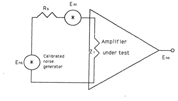
Figure 2.3.1 shows the block diagram for measuring the input noise. Vs represents the input sine wave signal or sine wave genera-tor. Eni is the equivalent input noise, which is being measured. Zs
is the source impedance. The system is represented by the amplifier symbol. The equivalent output noise, Eno, and the output sine wave signal, V are measured at the output terminal of the system.
z
Source: [2.274]
Figure 2.3.1 Sine Wave Method of Noise Measurement
The gain of the system, Kt, is equal to
Kt - Vo (2.3.1)
Vi
The gain is measured by inserting the sine wave voltage generator, V, in series with the source impedance, Z, at the input of the system. The resulting sine wave is measured at the output terminal. The gain
is found using equation (2.3.1).
The output noise of the system, Eno is measured by removing the signal generator, Vs, and replacing it with a shorting plug. The source impedance, Zs, is not removed. The noise at the output of the system is measured with an rms voltmeter. Finally, the equivalent input noise is found using the following equation
Eni Eno (2.3.2)
Kt
frequencies, since the measurement procedure remains the same at all frequencies. The gain of the system at different frequencies is obtained by applying sine waves of different frequencies to the
system. This method can be used for low frequency noise measurements. The method may be useful for determining the noise and especially the gain of our noise measurement system.
2.3.2 Noise Generator Method of Noise Measurement
Measurement of the equivalent input noise of a system, will also be used to demonstrate how the noise generator method of noise
measurement works. Once again Motchenbacher and Fitchen [2] will be consulted for their description of this measurement method. The input noise measurement procedure is as follows:
1. Measure the total output noise.
2. Insert a calibrated noise signal at the input to increase the
output noise voltage by 3 dB.
3. The noise generator signal is now equal to amplifier equiva-lent
input noise. [2]
Figure 2.3.2 shows the block diagram for the noise generator method. Es, a calibrated noise source is placed in series with a sensor resistor, Rs. Eni represents the equivalent input noise of the system, the quantity that will be found using this procedure. Zi is
noise of the amplifier and the noise of the generator. An alternative setup for this method is to replace the calibrated noise generator Ens with a high-impedance noise current generator in parallel with the
source impedance Rs. Then the equivalent input current noise Ini may
E ni DI
Ens
Source. 2.2881
be calculated.
In the noise generator method, the output of the system is measured twice, one time with the noise generator in place and the other with the generator disconnected. The first step in the measure-ment is to measure the noise at the output of the system with the noise generator disconnected. Then attach the generator to the
system. Adjust the output of the generator until the output noise of the system is twice the value it was before, or in other word, 3 dB higher than before. Now measure the output of the noise generator. This value is equal to the equivalent input noise of the system.
The advantage of the noise generator method is the ease of the measurement, just attaching a noise generator to the system and
adjusting its value until the output is doubled. Another advantage is that the method is inexpensive, because a low cost diode could be used as the noise generator.
There are disadvantages to this method as well. It is not well suited to low frequency measurements because long measurement times are required. Also pickup of additional noise at the input terminals is more likely to occur in this method, because of the system con-figuration.
2.3.3 Correlation Method of Noise Measurement
The correlation method of noise measurement is especially useful for measuring very small noise signals. Unlike the other two methods of measurement, this method does not measure or calculate the
equiva-lent input noise or gain of a system. Instead it measures a noise
signal. It could be used to measure the output noise of a system, but
other methods would have to be employed to find the input noise and
gain of the system.
The best description of the correlation method is given by A. van der Ziel [3]. Figure 2.3.3 shows the measurement setup for this method and was taken from A. van der Ziel's book, Noise in Solid State Devices and Circuits. The first step in the measurement is to feed the signal to be measured, Vn, through parallel amplifiers and
filters. The amplifiers are represented by A's in the figure and the filters by F's. The resulting signals, V1 and V2 are both amplified
and filtered. V1 and V2 are then put into a crosscorrelator. (See
Figure 2.3.3.) The crosscorrelator multiplies the two signals together and its output is the product of the signals, V1V2. This
signal is then averaged over a certain period of time by the averaging circuit. (See Figure 2.3.3.) The output of the averager is V1V2.
When the signal is averaged, the noise of the two amplifiers dis-appear, since they are uncorrelated. The signal that remains, V1V2,
r1T
I
-. M II
[ A
i{~~~~~~
[7
J-~V2
(I:)V
n 0 Correlator V V2 Averaging VI V2 4 -, . 0 4 Ir)
that remains, V1V2, is equal to the signal being measured.
There are several advantages of the correlation method. First, the method allows measurements of very small noise signals. Second, the measurement system for this method is more stable against drift, because the system noise is eliminated from the output noise. For our
needs the method may be useful, if the signal we are measuring is small. The method may also be useful, if stability of our measurement system limits the accuracy of our measurements.
2.4 Typical versus State-of-the-Art Noise Measurements
Due to the limited applications, precision noise measurement is not a common area of study. One need for noise measurements is the classification of semiconductor devices. Semiconductor manufacturers often produce low noise components. Applications for these components include systems with low level inputs, audio systems and noise
measurement systems. When a manufacturer says a component is low noise, they usually mean that the component is designed to have low noise and that the product sold has a noise level around a value
specified on the data sheet. The manufacturers need to perform noise measurements to verify the noise level predicted by design, to
determine the average noise level for the component and to screen out any component that does not have the specified noise level.
The noise measurements that manufacturers conduct on their com-ponents is what I refer to in this paper as a typical noise measure-ment. Some manufacturers use special equipment designed to measure
noise to perform their measurements. One such device is the Quan-Tech Model 5173 Semiconductor Noise Analyzer. With all available attach-ments, this device is able to measure noise in a variety of semi-conductor devices especially transistors (FETs and bipolars), diodes and operational amplifiers. By inserting a device into the
appropriate fixture, a user receives the noise level of the device at five frequency regions (10 Hz, 100 Hz, 1 kHz, 10 kHz and 100 kHz). This particular device is considered state-of-the-art for production screening, but its accuracy is not specified. Resolution is to 3 1/2 digits per reading. The accuracy or more precisely the resolution of the Quan-Tech is not good enough to detect slight differences in the noise levels of similar semiconductors. The ability to detect such a change is necessary for our project.
State-of-the-art noise measurements were conducted by Wieslaw A. Lukaszek in 1974, for his PhD. thesis from the University of Florida
[1]. He used noise measurements to investigate the transition from tunneling to avalanche breakdown in silicon p-n junctions. Lukaszek built his own noise measurement system by combining circuitry he built with commercial equipment. We consider his measurements and measure-ment system state-of-the-art because we know of no diode noise
measurements with better accuracy. He characterized the accuracy of his system using resistor noise measurements. The resistance values predicted from noise measurements were within 2 of values obtained from precision bridge measurements.
2.5 Lukaszek's Noise Measurements
For his doctoral research at the
University
of Florida,
Weislaw
Lukaszek investigated
the transition
from
tunneling
to
avalanching in
silicon
p-n junctions.
[1]
To study this
transition
he measured
the
electric noise produced by the diode (p-n Junction). The noise level of the diode reflects the ratio of tunneling to avalanche current within the diode. Lukaszek used V-I measurements to pinpoint the
transition between the two types of breakdown as well as to calculate
the multiplication factor for avalanche breakdown. The noise
easure-ments he made are the most accurate noise measurements to date.
For our project, we are interested in Lukaszek's noise measure-ments more than his experimental conclusions for several reasons. First, we are interested in knowing the ratio of tunneling to avalan-che current within the diode. Second, the 2 accuracy of his measure-ments is interesting, because we need to make highly accurate noise measurements. These measurements may have to be better than 2X accurate, but at least by following some of Lukaszek's ideas for measurement we should be able to achieve the 2 degree of accuracy.
Improvements in technology in the fifteen years between the measure-ments may make our measuremeasure-ments more than 2 accurate. Third, since Lukaszek's measurements are also conducted on diodes his work can be used as a reference to see if our system is working as it should.
In this section, Lukaszek's noise measurement system will be described. His measurement procedure will be outlined. In addition, noise ratio and how it can be used to distinguish tunneling from
2.5.1 Lukaszek's Noise Measurement System
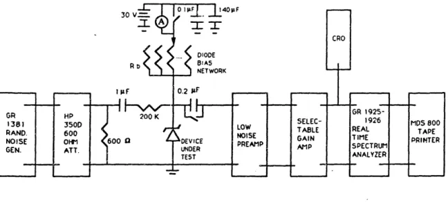
The system that Lukaszek used to make his noise measurements may be seen in Figure 2.5.1. The General-Radio 1381 Random Noise Genera-tor along with the Hewlett-Packard 350-D attenuaGenera-tor is used to provide a white noise calibrated signal to the system. The 600 n resistor, located after the attenuator, is used to provide an impedance match between the attenuator and te rest of the system. The capacitor and
resistor in series provide DC and impedance isolation from the rest of the circuit. This isolation is necessary to maintain a constant
impedance at the attenuator output terminals regardless of the diode bias network and to convert the noise calibration network into a high
impedance current-like source that will not load the diode. The diode bias network is a variable current source. Low noise wire wound
resistors, Rb, may be switched in and out of the circuit to provide a range of bias currents to the diode. At the output of the diode is a specially designed preamplifier circuit that utilizes a low noise JFET. After this preamplifier is a selectable gain amplifier which is used to amplify the noise signal so it may be detected by the General-Radio 1925-1926 Real Time Spectrum Analyzer. This instrument consists of 45 third-octave filters, ranging in center frequencies from 3.15 Hz to 8 kHz. The output of each filter is sampled for up to 32 seconds and the rms voltage of each filter, in units of dB, is computed and displayed on the General-Radio 1926 or printed out on the MDS 800 tape
30V 1011L.L L4DF 30 V _ A F CR DIODE
R
<
AS
NETWORK I_..r _f uF GR 1381 RAND. NOISE GEN. HP 200 K 350D 1 LOWAOHM 00 DEVICE PREAMP
ATT. UNDER TEST
~~~
-~~~~ SELEC-TABLE GAIN AMP 1 GR 1925-1926 REAL T IME SPECTRUM ANALYZER _ MDS 800 TAPE PRINTER Source: [1:1 05]Figure 2 5 1 Lukaszek's Noise Measurement System
2.5.2
Measurement Procedure
Lukaszek used the following procedure to make his noise measure-ments. First, he removed the noise calibration signal provided by the General-Radio 1381 and the attenuator from the system by disconnecting the attenuator. He placed a 600 resistor in parallel with the 600 n resistor already in the circuit. The diode was biased at a specified reverse current. Then a series of five, 32 second, measurements of the diode noise were made. The next step was to take the second 600 resistor out and reattach the attenuator to the system. The attenua-tion level was adjusted so that the output noise was 20 dB higher than the diode noise output alone. Another set of five, 32 second,
measurements were made. From his noise model for his system and the measurement he made, Lukaszek was able to determine the noise current
Lukaszek verified the accuracy of his system by measuring
resistors in place of diodes. He followed the same procedure as out-lined above. Using diodes in the range from 200 n to 2 M he was able to predict resistance values from the noise data, that agreed to
better than 2 with values obtained by precision bridge measurements.
2.5.3 Noise Ratio
Lukaszek calculated the noise ratio (See Appendix A for defini-tion) for each diode from the noise and reverse current data he
measured. The noise ratio indicates whether the breakdown of the p-n junction is caused by tunneling or avalanching. A single step ing process has a noise ratio of exactly unity. Multiple step
tunnel-ing processes have a noise ratio of less than unity. Noise ratios
larger than unity indicate that there is some avalanche breakdown. As
one can see from Lukaszek's thesis, noise ratio can be used as an
indicator of the transition from tunneling to avalanche breakdown within diodes.
Section 3 DESCRIPTION OF THE NOISE MEASUREMENT SYSTEMS
3.1 The First Measurement System
3.1.1 Block Diagram
The block diagram for the first noise measurement system may be
seen in Figure 3.1.1.1.
The system has two components, a circuit
and
Circuit
(Current source, DuT. amplifiers, filter)
Figure 3.1.1.1 Block Diagram for the First Noise Measurement System
the Hewlett-Packard 3562A Dynamic Signal Analyzer (HP 3562A). The
system
is
not
as simple as it appears because each component has
several parts and plays several roles in the overall measurement. More detailed descriptions of the components are contained in the fol-lowing sections. A brief outline of the system is presented here.The circuit portion of the system has three major parts; a
current source, the device under test (DUT), and a noise amplifier. The current source is variable and is used to bias the DUT. The noise amplifiers, as their name suggest, amplify the noise signal produced by the DUT. Amplification is necessary to make the noise signal large
enough so that the noise measuring device (in this system the HP 3562A) may detect the signal.
The Hewlett-Packard 3562A Dynamic Signal Analyzer performs several tasks within this measurement system. First, it provides bandlimiting for the system by allowing the user to choose the band-width of the noise measurement. Second, the HP 3562A is used in the calibration process for the system. In particular, the HP 3562A sup-plies a signal to the circuit and makes a measurement of the frequency response of the circuit. The gain of the circuit may be determined
from
this frequency response.
Third,
the
frequency
response
measure-ment capability of the HP 3562A is used to determine the incremental resistance of the DUT. Finally, the HP 3562A is used to measure the noise signal at the output of the circuit portion of the system.3.1.2 Circuit Description
The circuit portion of the first system consists of a variable current source, a calibration input, a socket for the DUT, three noise amplification stages and a filter. All of these sections are con-tained in one box. The circuit diagrams for this portion of the
t--2
L44 VY I .10 6I .1
- o ,
C-6 . 11 I I- 4
II
o 0OI
I .
:_~~~(a..--100
-
0 -T
o C. -t-I
O 6r-
a
II E U L (.) , L o,a-II
I.; C a-r q. I I6d6 6 t, 4 O
1
'I,
-I
I~~'
0 ! I C 0 ID 4. I0 0 o L) 0 V) .-C . 0 rr 0 t-CN L. v'U.
1Aw1
iI
?
1 I ICP
-i H .J1
e 'r
30
"-E m, 11 vL III LLI
t s " i 'SI-3 D- A-iI C. e & am. Jw ,. 0 I U -L I Q. E Li 0 LL 4 J 'pf. I 4. a-I1I --4 %. to e2 ;6 at 'a . t
system may be seen in Figures 3.1.2.1 through 3.1.2.4. Figures 3.1.2.1 through 3.1.2.3 show sections of the circuit, while Figure 3.1.2.4 shows the complete circuit. Each section will be described in further detail in the following paragraphs.
The bias circuit was designed to have several features. The circuit has constant power dissipation, independent of bias current. Bias current is insensitive to the voltage of the DUT. The bias
current needs a temperature controlled reference voltage for the input in a feedback configuration so it is stable. It is also easy to
filter out high frequency noise from this circuit.
The bias circuit may be seen in Figure 3.1.2.1. A National Semiconductor LM399 voltage reference provides a constant voltage of 7 Volts to the bias circuit. The purpose of the complex circuitry that
follows the voltage reference is to keep the voltage from the output of the U2 op amp to the noninverting input of the U3 op amp (From points A to B on Figure 3.1.2.1) constant. In other words, the voltage across the bias resistor network is kept constant. Resistor values within this network range in from 499 Qf to 2 Mn. These
resistors may be switched into the circuit to produce a variety of bias currents for the DUT. The selected bias current then flows
through a 100 resistor used to measure bias current and into the DUT itself.
The next two parts of the circuit may be seen in Figure 3.1.2.2. They are the cal(ibration) input and the DUT socket. The CAL input as its name implies is the point in the circuit where a calibration
passes into the amplification stages at the top of the DUT. Since diodes are the type of devices being measured in this system, the DUT socket is one that accommodates such a device. The cathode of the DUT is attached to the 1000 resistor and the anode is attached to ground. The DUT is reversed biased.
There are three noise amplification stages within the circuit. When designing a noise amplification stage one must design a low noise amplifier because you do not want the noise of the amplifier to swamp the noise signal you are amplifying. To keep the noise of the
amplifier down, one can use low noise operational amplifiers, which have low input noise voltages and currents. These low noise opera-tional amplifiers are especially critical in the first amplification stage where the input signal is very small. In this circuit, the Linear Technology LT1028 low noise operational amplifier is used in the first and second amplification stages.
The three amplification stages may be seen in Figure 3.1.2.3. The input of the first amplification stage is the sum of the noise of the DUT and any calibration signal. The first stage has a gain of approximately 101. The second stage also has a gain of approximately 101. The last stage is not only an amplifier, but also a filter. The gain of this stage is 3.16. The filter is a second order low pass filter with a cutoff frequency at about 263.6 kHz. The amplified noise signal passes though a simple high pass filter with a cutoff at
7 Hz. This filter eliminates any DC signal. Then the amplifier signal goes to the output terminal of the circuit.
3.1.3 Commercial Equipment
There is only one piece of commercial equipment used in this measurement system. This is the Hewlett-Packard 3562A (HP 3562A). This piece of equipment is used to calibrate the system, measure the gain of the system, and measure the noise of the system. From the range of functions the HP 3562A performs, it can be seen that this is a very versatile piece of equipment. In this section, the measurement procedures for frequency response and power spectrum measurements with the HP 3562A will be described in detail. Pertinent specification for the HP 3562A will also be presented.
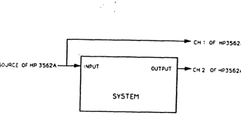
The HP 3562A is capable of making a frequency response measure-ment on a system. This measurement, sometimes called a transfer func-tion, is the ratio of the system's output to input. From this
measurement, the gain and phase shift of the system may be determined. The basic setup for the frequency response measurement may be seen in Figure 3.1.3.1. The source output terminal of the HP 3562A is
I
- CH 1 OF P3562A OF,H352-
j
50JRCE OF HP 3562A INPUT OUTPUT CH 2 OF HP3562A
SYSTEM
attached to its own channel one and the input of the system. The output of the system is attached to channel two of the HP 3562A.
The HP 3562A offers four types of measurement modes; linear resolution, log resolution, swept sine, and time capture. Frequency response measurements may be made with the first three modes. For our measurement purposes, we conduct frequency response measurements in only the linear resolution and swept sine modes.
In the linear resolution mode, time data is sampled until a data buffer called the 'time record' is filled with a fixed number of time samples. Once a time record is filled, the fast Fourier trans-form of the record is computed and the frequency spectrum is
dis-played." [9:9] In this mode each channel has 801 lines of frequency
resolution. The resolution ranges from 125 Hz for a full (100 kHz) frequency span to 12.8 pHz for the smallest (10.24 mHz) frequency span.
In the linear resolution frequency response, a signal is applied by the HP 3562A through its source terminal to the input of the
system. There are five types of source signals to select from; random noise, burst random noise, periodic chirp, burst chirp, and fixed sine. The random noise and fixed sine are the most common selections. The source level may also be selected. The range of levels depend on the type of signal being applied.
The averaging capabilities of the HP 3562A may also be used with this measurement. There are four types of averaging available; stable (mean), exponential, peak hold, and continuous peak. We use only the stable (mean) type of averaging. Any number of averages between 1 and 32,767 samples may be selected . The HP 3562A makes a number of
measurements equal to the number of averages selected. It averages these measurements and displays the average value.
The frequency span of the measurement may also be selected. The frequency span of the HP 3562A is from 0 Hz to 100 kHz. Various
smaller frequency spans may be selected. If the frequency span of the system being measured is known, it should be used as the measurement's frequency span. If the frequency span of the system is unknown, it is best to use the full 100 kHz span.
Once the HP 3562A completes the frequency response measurement, it will display the magnitude (gain) versus frequency on the screen. The scale and units of the display may be changed. The cursors and special marker capabilities of the HP 3562A may be used to determine certain values, like the gain at certain frequencies. If the HP 3562A is attached to a plotter a copy of the screen may be produced.
Frequency response measurements are also made with the swept
sine mode.
In
this mode, the
HP
3562A is reconfigured as a
full-function DC to 100 kHz frequency response analyzer." [9:15] This type of product is traditionally used in low frequency network analysis. These products perform the same measurement as a tuned network ana-lyzer, but instead of using low frequency filters they "perform a time domain integration of the input signals to mathematically filtersignals at very low frequencies. Measurement results are usually dis-played as point-by-point numerical values or on an x-y plotter."
[9:15]
In a swept sine frequency response, the source that is applied to the system is a sine wave with a fixed amplitude, that the operator selects, and a varying frequency. The initial frequency of the sine wave is called the start frequency. The frequency of the wave changes at a certain rate called te sweep rate. The final frequency is equal to the start frequency plus the frequency span. The start frequency, sweep rate and frequency span may all be selected by the operator. The operator also has to choose between a linear or log sweep. The difference between the two is that the frequency is either linear or logarithmic. The frequency response for each frequency within the span is calculated and displayed on the screen. The frequency response is drawn on the screen a point at a time.
The swept sine measurement is like the linear resolution method in several ways. Averaging can be utilized, where in this mode
measurements at a single frequency are averaged and then displayed. The scale and units of the measurement can be easily changed with a touch of a button. The cursors and special markers may also be used with the measured waveform.
The other type of measurement made with the HP 562A is the power spectrum measurement. This measurement may be make in the linear resolution and log resolution modes. In our system we only make the measurement in the linear resolution mode. The power
spec-trum measurement displays the input signal in the frequency domain. It is computed by taking the FFT of the input signal and multiplying
it by complex conjugate of the FFT.
To make this measurement, attach the signal to be measured to either one of the HP 3562A channels. Then check to make sure the channel is activated. Display the power spectrum of the channel on the screen. Select the frequency span of the measurement. Decide if averaging is desired and if so select the number of averages to be made. Start the measurement.
Once the measurement is completed, the power spectrum is dis-played on the screen. The units and scale can be changed so the desired spectrum is displayed. The cursor and special markers can be utilized to record more detailed data. Since the power spectrum measurement is used to measure the noise of the system, the units of Volts2/Hertz is selected. If these units are used the displayed waveform is equal to the spectral density of the noise signal.
This section has just briefly described two types of
measure-ments made with the HP 3562A. Along with these descriptions, some of
the specifications of the HP 3562A have been given. A complete
listing of the specification of this device may be seen in Appendix D. The specifications will be discussed again in section 4, when I
3.1.4 Measurement Procedure
A calibration procedure is part of the overall measurement pro-cedure. The calibration procedure measures the gain of the system as well as the noise of the system for three calibration resistors (10, 100 and 1,000 ohms). This data is then fed into a computer program which returns several constants. The constants are ultimately used to
determine the dynamic resistance and the noise ratio associated with the DUT.
The circuit and the HP 3562A are the components involved in the calibration procedure. The capabilities of the HP 3562A are utilized in this calibration procedure. In particular, the HP 3562A is used to make frequency response and noise (power spectrum) measurements. The mathematical functions as well as source capabilities are used in con-junction with these measurements.
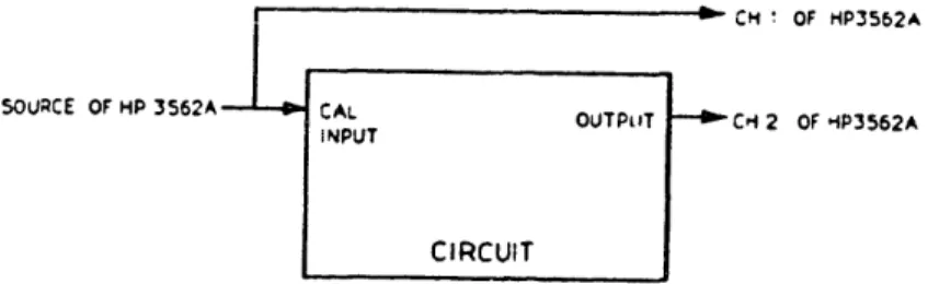
The first step in the calibration procedure is to measure the frequency response correction waveform. This correction waveform is necessary for measurements made outside the original measurement band-width, a bandwidth in which the frequency response of the system was adjusted to be flat. It was discovered that some of the devices being measured by the system displayed 1/f noise above 5 kHz. To measure the noise of such devices, without added 1/f noise, it was necessary to use other bandwidths. A technique, which employs a correction waveform, allows the frequency span to be moved without modifying the hardware of the system.
The setup for the measurement of the correction waveform may be seen in Figure 3.1.4.1. The source of the HP 3562A is attached to the
SOURCE OF HP 3562A CAL -- COUTPUT C 2 OF HP3562A INPUT
CIRCUIT
CH I OF P3562A -- VOLTAGE
Figure 3.1.4.1 Setup for Correction Waveform Measurement
CAL input of the circuit. The VOLTAGE terminal of the circuit is
attached to channel 1 of the HP 3562A, while the OUT
terminal of the
circuit is attached to channel 2.
The 1 k calibration resistor is used as the DUT in the correc-tion waveform measurements. The 16 k bias resistor is put into
place, producing a bias voltage of around 0.4 mV. The HP 3562A is set for a sweep sine frequency response measurement using state 3, which may be seen in Figure 3.1.4.2. The frequency range in this state must be adjusted so it corresponds to the range which will be used in
future noise measurements. A series of ten sweep sine measurement, with HP 3562A calibrations between each measurement, is taken. The
Swept Sine
AVERAGE: INTGRT TIME 50. OmS
FREQ:
START
STOP 5 55 kHzkHz
SWEEP: TYPE DIR
Liner .
Up
9 AVGS
SPAN 50.OkHz RESLTN 31.2 Hz
EST TIME EST RATE
12.1
Mn 68.7 Hz/S
AU GAIN: Off ENG UNITS . 0 V/'EU.
0 V/EU
COUPLINGAC
(Flt)
AC (Flt) LEVEL OFFSET 450mVpk 0.0 VpkFigure 3. 1.4.2 State 3, Used for Frequency Response Measurement
purpose is to average calibration effects. This series of measure-ments is easily made by using the auto sequence titled "Start w/Cal", which may be seen in Figure 3.1.4.3. When all
Auto Seoquence 4
Display ON Lebel: START W/CAL
I START
2 SAVE RECALL: SAVE DATA#
3 CAL: SINGLE CAL
4 ASEQ FCTNS: TIMED PAUSE
5 START
6 MATH: ADD: SAVED 2
7 ASEQ FCTNS: LOOP TO 2. 8
8 MATH: DIV 10
174
Keys Left
2
0 Sec
Figure 3.1.4.3 Autosequence "Start w/Cal"
I
IIPUT:
CH 1 CH 2 'SOURCE: RANGE 3.99mVpk11.2 Vpk
TYPE
Of ften measurements are displayed the frequency response is displayed on the screen of the HP 3562A. The frequency response is manipulated to obtain the absolute magnitude squared gain. The HP 3562A has two display traces, A and B. A measurement may be displayed in either of both of these displays. The manipulation of the frequency response utilizes the dual trace capability of the HP 3562A. First, the fre-quency response in both trace A and B. Trace A is complex conjugated
and multiplied by trace B. The result is the absolute magnitude
squared gain of the system for a particular bandwidth. This result is stored in the HP 3562A's memory within Data 1. All future noise measurements made within this frequency range should be divided by
this correction waveform. By doing this, the noise data is corrected for any effects of the noise amplifier outside its flat region and is referred back to the DUT.
The next step in the calibration procedure is to measure the gain of the noise amplifier from the CAL input to the OUT terminal at a fixed frequency of 5.2 kHz. The setup for this measurement may be seen in Figure 3.1.4.4. The source of the HP 3562A is attached to its
i b CH OF HP3562A
SOURCE OF HP 3562A AL OUTPIT CH 2 OF HP3562A
INPUT
CIRCUIT
own channel 1 and to the CAL input of the circuit. The OUTPUT termi-nal is attached to channel 2 of the HP 3562A.
The 1 k calibration resistor remains as the DUT. The source
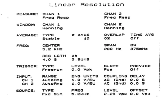
level of the input sine wave is adjusted so that the sine wave at the output of the circuit is around 1.6 V. This is ust a conventional value and does not have to be exact. The HP 3562A is set up for a linear resolution frequency response measurement using state 2, which may be seen in Figure 3.1.4.5. Using the auto sequence "Start w/Cal" a series of ten
Linear
Resolution
MEASURE: CHAN CHAN 2
Freq Resp Freq Resp
WINDOW: CHAN CHAN 2
Henning Henning
AVERAGE: TYPE # AVGS OVERLAP TIME AVG
Stable
10
0x
Off
FREQ: CENTER SPAN BW
5.2 kHz 200 Hz 375mHz
REC LGTH At
4.0 S 3.91mS
TRIGGER: TYPE LEVEL SLOPE PREVIEW
Freerun 0.0 Vpk Poe Off
INPUT: RANGE ENG UNITS COUPLING DELAY
CH 1 AutoRng 1.0 V/EU AC (Gnd) 0.0 S
CH 2 AutoRng i.0 V/EU AC (Gnd) 0.0 S
SOURCE: TYPE FREQ LEVEL OFFSET
Fxd Sin
5.2kHz
2.25 Vpk
0.0
Vpk
measurements with calibrations in between are taken and averaged.
This average frequency response should be displayed on the screen and
the value at 5.2 kf should be recorded. This is the gain from the CAL input to the OUT terminal.
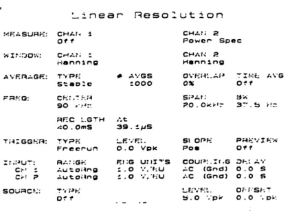
The third step in the calibration procedure is to measure the noise of the 1 k calibration resistor using the HP 3562A. The system may be left in the frequency response setup that was seen in Figure
3.1.4.4. The source is not used in this case and only channel 2 is activated. The HP 3562A is set up for this noise (power spectrum) measurement using state 1, which may be seen in Figure 3.1.4.6. The
Inear Resout
oon
?.iE;SUii: CHAtr. CICA?. 2
Of f Power Spec
W I: i:O: CoAt; - CHANt 2
Hnning
Henning
AV'F RAGF: TYPF * . GS OV'F;4' - .:i:. AVG
StbaC '000 OX Off
'. Q:
CF-:
.-. ;4
S;=&,t
v,'^
90
PO'.:
20.0
.
'-
3
7.
i!-.
iFIC .GTH ,At
40. OmS 39. !.S
T;4GG'F:i: TYPE '. F','F:. St OPF- PiV:'/I F-W'
Frecrun 0.0 Vk Po* Off I:;; U: f;:: G . : Fi G U:IIS COUPI.. I.G DF.: a' '
C' ' : Auto;4ng : .O '.'F:U C (Gnd) O.O S
Ci -; uto;.ng ' .'I,'U ;.C (Gndc) 0.0 5
SOLURCF.: T',; i- LE" '':L. OF; 'S: T
Of: . .I. '. D;
Figure 3. 1.4.6 State 1, Used to Measure Noise,
frequency range must be moved to the appropriate frequency bandwidth. The autosequence "Start w/Cal" is used with this measurement setup so a series of ten measurements with calibrations in between are made and
the HP 3562A memory. The special marker ave value' is pressed to display the average value of the noise for the 1 k calibration resistor. This value is in units of Volts2/Hertz.
The fourth step in the calibration is to estimate the resistance of the 1 kgl calibration resistor. This is done by measuring the
voltage across the resistor and the current through it with a meter. We use a Fluke 8506A digital volt meter for this job. The voltage is measured at the voltage terminal of the circuit and the current is measured at the current terminal of the circuit. The resistance of
the 1 k resistor is estimated using the following formula.
RDUT - TA * Rs (3.1.4.1)
CURRENT
Rs is the sum of the resistor which the current is measured across,
which has a resistance of 100 , and the resistance of the wire, which has a resistance of 0.0110.
Steps two through four of the calibration procedure are repeated with a 10 and a 100 calibration resistor used as the DUT. After these measurements are complete, a four terminal resistance measure-ment is made with the Fluke 8506A on all calibration resistors. The gain and noise data obtained from the three calibrations along with the corresponding calibration resistance are fed into the program cal.bas. A copy of this program may be seen in Appendix C. The program solves three linear equations for the calibration constants, Cr, G and Kr. The program also solves three linear equations for the
calibration constants A, B, and C. These six constants are used with noise measurement data obtained for diode DUTs to determine the
dynamic resistance and noise ratio of the DUTs.
Once a calibration is made, noise measurements on various DUTs can be conducted. The data from the calibration is used to solve for noise ratio and other parameters. Another calibration is not
neces-sary for several months or until something is changed in the circuit.
If changes are made to the circuit a calibration should be performed before the system is used again for noise measurements.
The -- asurement procedure used with this system begins with the installation of a DUT. The DUT is usually a diode, The DUT is biased at a certain current by switching in bias resistors until the desired current is reached. The bias voltage is measured with the Fluke 8506A at the VOLTAGE terminal of the circuit. The bias current is measured at the CURRENT terminal of the circuit. Actually the voltage across a 100 n resistor is measured. The bias current is obtained by dividing this voltage by 100 . The bias voltage and current data will be used later in the project to determine if there is correlation between noise and radiation characteristics of the diodes.
The next step in the measurement procedure is to measure the gain from the CAL input to the OUT terminal. This measurement is made at a fixed frequency of 5.2 kHz using state 2 (see Figure 3.1.4.5). This fixed gain is recorded and used along with the three calibration constants, G, Kr, and Cr, to find the admittance, Gd, which is equal
to the DUT
resistance in parallel with the bias resistors.
Gd is
found using the following equation.
cd
r
-
G
(3.1.4.2)
If the resistance is desired, it may be easily obtained by inverting this admittance (Rd - 1/Gd).
The last measurement made in this procedure is a measurement of the output noise of the circuit with the HP 3562A. A measurement of the noise spectral density, Sv, is made by performing a power spectrum measurement using state 1 (see Figure 3.1.4.6) on the output of the circuit. Sv is a noise voltage spectral density in units of
Volts2/Hertz. It contains a noise contribution of the circuit and the DUT. Dividing the spectral density by the correction waveform refers the noise back to the DUT.
Once the three measurement steps have been completed there is enough information to calculate the noise ratio of the DUT. See
Appendix A for a definition of and formula for noise ratio. To calcu-late noise ratio the noise voltage spectral density referred to the
DUT, Sv, will have to be converted into a current spectral density,
consisting of only the DUT noise, Sid.
The first step in this conversion is to subtract away the noise contributed by the circuit. The noise contributed by the circuit is dependent upon the impedance seen at the input of the noise amplifica-tion stage of the circuit. From the calibraamplifica-tion process three con-stants, A, B, and C were found. These constants are the coefficients of an equation that can be used to predict the noise at the DUT node
produced by the system. In the case of a diode DUT, the impedance
seen at the input of the noise amplifier is the resistance, Rt. Rt isdescribed by the following equation.
Rt - (1/Rd + G)
1(3.1.4.3)
Substitute the value for R
tinto
the following equation
e
0
2A + B * Rt + C * R
2(3.1.4.4)
allows
one to predict the noise of the system, eo. This
output
noise
is subtracted from S.Recall that the noise measured was a voltage spectral density. For noise ratio calculations, one needs a current spectral density. To obtain the current spectral density ust divide by the resistance seen at the DUT node, Rt. squared.
When the predicted noise e 2 was subtracted from S, e 2
included noise contributed by the incremental resistance of the diode. But this resistor is, by convention, modeled as noise free. So, we follow convention by adding a thermal noise current spectral density equal to
it2 - 4kT/Rd (3.1.4.5)
Thus the overall conversion of S
vto Sid may be summarized with
the following formula.
Sid -
e
2 + it2
(3.1.4.6)Now
with the spectral density, Sid, and the bias current, Ir, known,
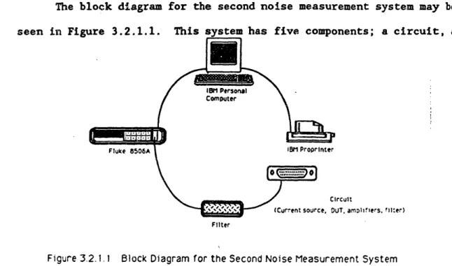
3.2 The Second Measurement System
3.2.1 Block Diagram
The block diagram for the second noise measurement system may be
seen in Fig%
>nents; a circuit, arcult
JT, amprn iers. fIl:er)
Filter
Figure 3.2. 1.1 Block Diagram for the Second Noise Measurement System
filter, the Fluke 8506A Thermal RMS Multimeter (Fluke 8506A), the IBM Personal Computer (IBM PC) and the IBM Proprinter (printer). Once again, more detailed descriptions of the components are contained in
the following sections. The more generalized description appears in