HAL Id: jpa-00246871
https://hal.archives-ouvertes.fr/jpa-00246871
Submitted on 1 Jan 1993
HAL is a multi-disciplinary open access
archive for the deposit and dissemination of
sci-entific research documents, whether they are
pub-lished or not. The documents may come from
teaching and research institutions in France or
abroad, or from public or private research centers.
L’archive ouverte pluridisciplinaire HAL, est
destinée au dépôt et à la diffusion de documents
scientifiques de niveau recherche, publiés ou non,
émanant des établissements d’enseignement et de
recherche français ou étrangers, des laboratoires
publics ou privés.
at low temperature. II: experimental study
F. Ladieu, D. Mailly, M. Sanquer
To cite this version:
F. Ladieu, D. Mailly, M. Sanquer. Conductance statistics in small insulating GaAs:Si wires at low
temperature. II: experimental study. Journal de Physique I, EDP Sciences, 1993, 3 (11), pp.2321-2341.
�10.1051/jp1:1993248�. �jpa-00246871�
Classification
Physics
Abstracts72.10B 72.15R 72.20M
Conductance
statistics
in
small
insulating
GaAs:Si
wires
at
low
temperature.
II:
experimental
study
F- Ladieu
(~),
D-Mailly (~)
and M.Sanquer
(~,*)
(~)
DRECAM/SPEC
CE-Saclay,
91191Gif/Yvette
Cedex,
France(~)
CNRS-LMM,
196 Av H- Ravera, 92220Bagneux,
France(Received
20April 1993,
received in final form 6July1993,
accepted
15July
1993)
RAsum4 Nous avons observ4 des fluctuations de conductance
reproductibles
dans un petit fil de GaAs:Siauquel
nous avons fait passer la transition d'Anderson parapplication
d'une tensionde
grille.
Nousanalysons
quantitativement lastatistique
log-normale
de conductanceen termes
de fluctuations
quantiques
tronqu4es.
Les fluctuationsquantiques
dues I depetites
variations del'4nergie
des 41ectrons(contr614e
par la tension degrille)
ne peuvent pas sed4velopper
complbte-ment I cause des fluctuations
g40m4triques
du r4seau de r4sistances assoc14 I la conduction parsauts dans l'4chantillon. L'4volution des
fluctuations,
suivantl'4nergie
des 41edtronsou le
champ
magn4tique,
montre que les fluctuations sont nonergodiques,
sauf dans le domaine d'isolantcritique
de la transition d'Anderson oi1lalongueur
de localisation estgrande
devant la distanceentre
impuret4s
de Si- Lamagn4toconductance
moyenne est en bon accord avec des simulationsfond4es sur
l'analyse
de "cherninsdirig4s",
c'est-I-direqu'elle
sature I In(°~~
~ ~~ -~ 1 poura(o)
a(o)
variant surplusieurs
ordres degrandeur
dans ler4gime
fortementlocalis4-Abstract We have observed
reproducible
conductance fluctuations at low temperature ina small GaAs:Si wire driven across the Anderson transition by the application of a gate
voltage.
We
analyse
quantitatively
thelog-normal
conductance statistics in terms of truncated quantumfluctuations.
Quantum
fluctuations due to smallchanges
of the electron energy(controlled
by
the gate
voltage)
cannotdevelop fully
due to identifiedgeometrical
fluctuations of the resistor networkdescribing
thehopping
through
thesample.
The evolution of the fluctuations versuselectron energy and
magnetic
field shows that the fluctuations arenon-ergodic,
except in the criticalinsulating
region
of the Andersontransition,
where the localizationlength
islarger
than the distance between Si
impurities.
The meanmagnetoconductance
is ingood
accordance with simulations basedon the Forward-Directed-Path
analysis,
I-e- it saturates toIn(a(H
>1)la(o))
m 1, asa(o)
decreases over orders ofmagnitude
in thestrongly
localizedregime.
Quantum
interference effects are not well understood in disordered insulators. This contrastswith the diffusive
regime
where their role in weak localization and of Universal Conductance Fluctuationsphenomena
has beenlargely
clarified boththeoretically
andexperimentally
iii.
However,
huge,
reproducible
conductance fluctuations have been observed for instance inthe
hopping
regime
of small Si:MOSFET [2] and inlightly
doped
GaAs:Sisamples
[3];
the conductance statistics are found to be verybroad,
giving
rise to veryhigh
conductance and resistancepeaks
(as
compared
to theaveraged value)
when the Fermi level or the transverseapplied
magnetic
field are varied.The mechanism of electronic conduction at finite low
temperatures
inlightly
doped
semi-conductors has beenexplained by
Mott [4]- Let us notekBTo
the levelspacing
on the scaleof the localization
length
(.
At low temperatures thehopping
electronsoptimize
the cost dueto thermal activation between energy levels of the initial and final
impurity
states and thetunnelling
term. This results in a Motthopping length given
rM, on average,by:
i
(
T~ d+1~° ~~ ~~' ~~
2 T ~~~
(d
thedimensionality)-The mean energy difference between the final and initial
impurity
levelsseparated
by
ro is:i i d
Eo
"-kBT~~+~
Td+1(2)
2
At very low
temperatures
rodiverges
and becomes muchlarger
thanI,
the distance betweenimpurities.
rM isthought
to be thephase
coherencelength
in theinsulating
regime.
Theaveraged
conductance in alarge
macroscopic
sample
isgiven
by:
1
To
d+12r~
g ~ exP
y
t exP~
(3)
One has to
distinguish
between twoexplanations
to describe the conductance fluctuationsversus electron energy in the
hopping
regime
of smallsamples:
fluctuations ofgeometrical
origin
due to achange
of theimpurity
sites visitedby
the electronstravelling
through
thesample
[5](incoherent
mesoscopic
phenomena [6]),
or quantum fluctuations due to interferencesphenomena
for a fixedgeometry
ofhopping
paths.
Firstly,
changes
in electronic energy could be sufficient to induce achange
of theimpurity
sites I and
j
between which the electronshop.
In other words rM fluctuates around ro when oneshifts the electron energy. As we will see, the
typical
energy range associated with such achange
is the Mott energyEo
(Eq. (2)).
Thequantum
tunnelling
resistancedepends
exponentially
onthe distance and on the energy
separation
of these sites [7] :~
~ ~~~
lEzl
+lEjl
+lEz
Ej1
~
in rj
~~~
"
2k~T
j
(E
= 0
corresponds
to the Fermilevel).
Because fewimpurity
levels are involvedduring
hopping
through
amesoscopic
sample
at very low temperatures, thelogarithm
of theconduc-tance itself exhibits
large
fluctuations. Theexplanation
oflarge
fluctuations versus theapplied
magnetic
fieldresults,
in thisgeometrical
approach, only
from Zeeman shifts of energy of theimpurity
states[2].
Secondly,
there exist conductance fluctuationsemerging
fromquantum
interference effects for a fixedquantum
coherenthop
(fixed
locations andenergies
for the initial and finalimpurity
states)
oftypical
size rM » I. Because of quantumcoherence,
one has to consider all theFeynman
paths
connecting
the initial and finalstates,
consisting
of multi-diffusionpaths
onintermediate
impurity
states. At T = 0K,
I-e- when the quantum coherencelength
is thelength
of thesample,
only
thesequantum
interferencespersist.
They
can beregarded
as fluctuationsof
(
itself. These fluctuations are influencedby
phase
shifts inducedby
anapplied
magnetic
flux.
Two models have been
proposed
to take into account the interference effects in thehopping
regime.
The first
approach,
referred to as Forward Directed Pathanalysis
(FDP),
neglects
explicitly
the quantum interferences between
returning
loops
due to backwardscattering
[8].
Thisap-proach
is aperturbative
treatment of thedeeply
localized electronic statesby
the intermediatescattering
during
hopping.
A crucialassumption
is that the localizationlength
is smaller than the distance betweenimpurities
(which
is itself much smaller than thehopping
distance).
In thissituation,
referred to in the rest of this paper as theregime
ofstrong
localization,
onehas to consider interferences between
Feynman
paths
ofsteps
+~I,
being
smallerthan rM. As
suggested
firstby Nguyen, Spivak
and Schklovskii(NSS)
[8],
only
the shortestpaths
the Forward Directed Paths areimportant,
because theamplitude
of transmissionalong
a Nllong
path
is affectedby
aprefactor
exp(f)
< 1(1If
>1),
exponentially
decreasing
with N.So the Forward Directed Paths
approaches
are welladapted
at least to thestrongly
localizedregime.
Thehypothesis (
< I excludes the criticalinsulating
regime
describedby
thescaling
theory
of the Anderson transition.The second
approach
is based on a Random MatrixTheory
(RMT)
applied
to the transfermatrix of either conductors or insulators
[9].
In thisglobal
approach
resonances as well asquantum
interferences between all sorts ofFeynman
paths
are apriori
included. To someextent, this
theory
indicates thatreturning
loops
within the localization domain areessential,
and thus is well
adapted
to the criticalregime
of the Andersontransition,
where(
»I,
I-e-when electrons are localized over manyimpurity
sites.FDP and RMT
predictions
differdrastically
forstrong
spin-orbit
scattering
or for the effect of amagnetic
field.The FDP
approach
predicts
the existence of alarge
positive
meanmagnetoconductance,
which is not the consequence of interferences between Time Reversal
conjugated
returning loops
(they
areneglected).
The meanmagnetoconductance
< In~~~~
>
depends
only
on To(10],
g(0)
and is
always
positive
whatever thespin-orbit
scattering
strength.
The FDPapproaches
alsopredict
large log-normal
conductance fluctuations which are smaller versus themagnetic
fieldthan versus the disorder
configuration
(non-ergodicity)
[8].Quantitatively,
theamplitude
of thefluctuations
var(In(g))
versus disorder isgiven by
[11]
:var(In(g))
+~r(~
with w =1/3
(resp.1/5)
for d= 2
(resp.3).
By
contrast with the FDPapproach,
the basicsymmetries,
such as the Time Reversal andSpin
Rotation symmetry, arejust
the essentialingredients
in the Random MatrixTheory.
This
approach gives
exact resultsonly
inquasi-id
geometry,
and itsimplications
have to be weakened inhigher
dimensions. Nevertheless numerical simulations in 2d and 3dsamples,
as well as
previous
experiments,
yield
conclusions which are similar to some extent to exactRMT results
[12].
Moreover similar conclusions are obtained in d = 1,2,3
on acompletely
different model in[13].
The mainpredictions
of the RMTapproach
are that thebreaking
of the time reversalsymmetry
induceschanges
in the localizationlength
(,
andconsequently
anon the
spin-orbit
scattering
strength,
going
frompositive
tonegative
when thespin-orbit
scattering
increases. Thistheory
alsopredicts
log-normal
fluctuations but with a variance of thelogarithm
of the conductance which is related to the mean of thelogarithm
of conductance(this
is a one-parameter
theory):
var(In(g))
= <In(g)
>+~L/(
[9]. Note thatcontrary
tothe FDP
result,
the fluctuationamplitude
as well as the meanmagnetoconductance
depends
on
L/(,
and notonly
on L(L
+~ To atfinite
temperature).
The fluctuation isergodic
versusthe
magnetic
field and the disorder[14].
It is the aim of this work to test
experimentally
thevalidity
domain of bothapproaches,
by
addressing
the meanmagnetoconductance
effect,
the distribution of the conductance fluctua-tions and theergodicity.
A submicronic disordered GaAs:Si wire is driven across the metal-insulator transitionby
application
of agate
voltage.
The conductance of the wire is measuredover many orders of
magnitude
from the diffusiveregime
to thestrongly
localizedregime
atvery low
temperatures.
To some extent our observations are similar topreviously
reported
re-sults
[2, 3],
butsample,
analysis
andinterpretations
differnoticeably.
In short but wide GaAs MESFET used in reference[3],
the conductance is dominatedby
a few most conductivepaths,
whereas in our lD structure(see
also Ref.[2])
the resistance is dominatedby
one most resistivehop.
In Si-MOSFET used in reference[2],
the effect of amagnetic
field isinterpreted
in terms of Zeeman energy shifts in contrast to our observation of aquantum
coherent contribution.This, paper is
organized
as follows: in the first part we describe oursample
and thevicinity
of the metal-insulator transition when the
gate
voltage
VG is varied. This part includes weak localization fits in the diffusiveregime,
whichpermit
the determination ofL~
=fi,
thephase
coherencelength
and the effective width of the wire(D
is the diffusionconstant,
T~ thephase-breaking
time).
The rest of the paper is devoted to theinsulating
regime.
First,
westudy
thetemperature
dependence
of the conductance. We showthat,
becauseof the one-dimensional
geometry
of oursample,
its behavior withtemperature
is nevergiven
by
the usual standard Mott law.Indeed,
weexplain
that fluctuations of thehopping
length
around To cannot be
neglected.
The conductance of oursample
in thestrongly
localizedregime
is dominated
by
anexponentially
small conductancecorresponding
to ahopping
distance muchlarger
than the mean Motthopping length
To =< TM > These considerations areimportant
to
explain
somestriking
experimental
observations.We then turn to the
study
of thelognormal
conductance fluctuations themselves. Those inducedby varying
the chemicalpotential
are shown to result from a subtleinterplay
be-tween
geometrical
andquantum
fluctuations("Truncated
Quantum
Fluctuations",
[15]).
Sincequantum
fluctuations cannotdevelop
fully
as the Fermi energyshifts,
we turn to thestudy
offluctuations induced
by
theapplication
of amagnetic
field H and show thatthey
are of quan-tumorigin.
Ergodicity
and meanmagnetoconductance
behaviorschange
with theproximity
of the metal-insulator
transition,
and thispermits
us toclarify
thevalidity
domains of FDP and RMTapproaches.
1. The metal,insulator transition in our
mesoscopic
wire.1.I SAMPLE AND EXPERIMENT. The
sample
is a standard Hallbar,
with a distancebe-tween successive arms of 3 pm, obtained
by
etching
of aSi-doped
GaAslayer.
Thelayer
is400 nm thick grown
by
Molecular BeamEpitaxy
with a Si concentration of 10~3m~3
on a GaAssemi-insulator substrate. Electron Beam
Lithography
has been used to pattern thesample.
Thesubsequent
mask was used to etch the activelayer using
250 V argon ions. The width of thesample
isapproximately
400 nm. A 100 nm thick aluminiumgate
has beenevaporated
onThe
sample
isplaced
in theplastic mixing
chamber of aqompact
home,made dilutionrefrig-erator. For electrical
measurements,
coaxial cables are used between 300 K and 4K,
andstrip
lines between 4 K and the
mixing
chamber. All the lines areproperly
filtered. The resistanceis obtained
by measuring
the DC currentpassing through
thesample
with aKeithley
617 electrometer. The controlled excitationvoltage
supplied by
the electrometer isdivided,
and the I V nonlinearities have beenprecisely
studied(see later).
The electrometer is controlledby
computer,
and each measurementcycle
consists of10voltage
inversions followedby
a 3 swaiting
time and 6 measurements(conversion
time 0.3s.).
So the resistance results from anaverage of 60 measurements. The offset
voltage
isapproximately
100pV
for very different measured resistances. We have not detected any offset current.At very low
temperatures
inmesoscopic
samples,
one has to be very careful about excitationand offset
voltages
applied
across thesample
[I].
A commonproblem
is to measurelarge
resistances with excitation
voltages
smallenough
to be in the linear I Vregime.
Figure
I shows atypical
I V curve obtained at T= 91 mK in our
sample.
The characteristic is well fittedby:
1= A shl~~
~/~~~
with A = 4 x10~~~
A,
B = 5 x10~~
V(5)
and(~~~t
= -2 x10~~
V. The conductance isgiven by:
~
~Vd~+(ffa~t=0
~ ~ ~~ ~ ~ ~~~ 200 1 ~ --3 vThe
low-temperature
conductance of thesample
depends
on thehistory
of thecooling
downfrom room
temperature.
In other words the conductance forl§
= 0 Vdepends
for instance onwhether the
sample
has been cooled under V~= +I V or under V~ = -I V. The conductance is
systematically
larger
in the latter case. Therepersist
long
time relaxations at T = 4 Kafter a
large
variation of V~. Asystematic
study
permits
us to conclude that this relaxation isnot due to a
dynamic
of disorder seenby
theelectrons,
but to a slow variation of the Fermilevel. IA
fact,
after alarge cycling
inVG,
the observed conductance fluctuationpatterns
aretranslated in V~ but not at all decorrelated. This is consistent with a retarded response of the number of electrons to
large changes
ofVg,
with the disorderconfiguration unchanged.
One canqualitatively
take the observed facts into accountby
supposing
that thecharge configuration
ofelectronic
traps
inside thedepletion
barrier under thegate
is not theequilibium
configuration
corresponding
to the nominal V~ at lowtemperatures.
The difference results from the slow kinetics oftrapping
and release processes for the electrons at lowtemperature.
Thecharge
configuration
in thedepletion
layer
influences the number of electrons and the Fermi energy in the center of the wire.These relaxations can be avoided
by
restricting
the range ofgate
voltage
changes
in agiven
experiment
at low temperature, or if notpossible, by varying
thegate
voltage
back andforth a few times in the
corresponding
range before theexperiment.
With thehelp
of theseexperimental
procedures
the conductancepattern
isfully
reproducible
aslong
as thesample
is
kept
below T = 4 K.1.2 THE DIFFUSIVE REGIME.
Figure
2 shows themagnetoconductance
observed at lowtemperatures
for alarge
gate
voltage
VG,
such as the conductance of the wire which isrelatively
large.
For this value ofVg,
thetemperature
dependence
of the conductance is weak below T= 4.2 K. It is
impossible
to fit thisdependence
with a variable rangehopping
activation law(as
we will do in theinsulating regime),
because itgives
too smallTo
parameters
(for
instance
To
ci 50 mK < T for VG " 1.8V).
We fit the mean behavior of thelarge
positive
magnetoconductance
with standard ID weak localization formula [16] and we findL~
= 130 nmand an effective cross section
W~
=
(65 nm)~ (the
sample
has been rotated in themagnetic
field and themagnetoconductance
is found to be the same, which indicates that the crosssection is
isotropic).
The effectivelength
of thesample
is evaluated to be 5 ~Jm, because in ourtwo-probe
measurement apart
of two thin arms under thegate
contributes to the conductance.The
magnetic
fieldHc
whichgives
a fluxquantum
through
L~W
isHc
= ~= 0.42 T.
e
L~W
This
gives
thegood
order ofmagnitude
for the correlation field of themagnetoconductance
fluctuations. Theamplitude
of thefluctuations,
ifthey
aresupposed
to be the Universal ConductanceFluctuation,
isgiven by
ii?]
6g(H)
ci~~ ~
~~
~ ci 2.2x10~~
~~ in h~
hgood
accordance with theexperiment.
Figure
3 shows the variation of the conductance(in
units ofe~/h)
as a function of theapplied
gate
voltage
for T= 100 mK. The conductance exhibits
reproducible
Gaussian fluctuations as a function ofVG,
ofamplitude
similar to the conductance fluctuations inducedby
the transverseapplied
magnetic field,
and so in accordance with the estimate of the Universal ConductanceFluctuation.
In accordance with the
scaling theory
of the Andersontransition,
weexpect
that thetran-sition occurs for a conductance at the
phase
coherencelength
of ordere~/h.
For oursample
consisting
approximately
ofL/L~
ci 40quantum
boxes inseries,
this criterioncorresponds
to a conductance of order 2.5 x10~~
e~/h,.
Thiscorresponds
to agate
voltage
ofapproximately
o. oso 0. 045 0. 040 2
~
0. 035 co 0. 030 0. 025 0. 020 0 0. 5 1. 0 1. 5 2. 0 2. 5 3. 0 3. 5 llgslaslFig.
2.Magnetoconductance
(in
units ofe~/h)
at T= 100 mK for
large
positive VG = +1.8 V(diffusive regime).
The solid line is the lD Weak localization fit. The vertical bar is the UCF estimate.0. 0450 0. 0425 0. 0400
/
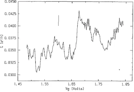
0. 0375 ~w co 0. 0350 0. 0325 0. 0300 1. 45 1. 55 1. 65 1. 75 1. 85 Vg lvol LslFig.
3. The conductance(in
quantumunits)
as function of VG in the diffusiveregime.
The verticalbar is the UCF estimate.
l§
= +0.5 V above which the
temperature
dependence
of g is weak between T = 4.2 K and T= 100 mK and
roughly
independent
of Vg. Below V~ = +0.5V,
g becomes activated: forinstance,
fromfigure
5,
we obtaintypically
that the resistance ratio between T = 4.2 K andT
+0.3 and +0.2 V. From the
experiment
it will bepointless
to argue any further about theexact
position
of the transition.Note nevertheless that in this range of
conductances,
the conductance fluctuationdeparts
from its value in the diffusiveregime, growing
andbecoming
asymmetric
with tails to lowconductances.
With the estimated effective cross
section,
andsupposing
that the concentration of electronsis close to the critical concentration- in GaAs for the Metal-Insulator Transition nc
= 1.6 x 10~~
m~~,
we find amobility
of~J ci 3600
cm~/Vs.
Close to thetransition,
we obtain thatlF
Cf 65 nm, which iscomparable
to the width of thesample,
EF
Cf 45K,
the elastic meanfree
path
ci 24 nmcomparable
to the distance between Siatoms,
andkfl
ci 2(Ioffe-Regel
criterion for the Metal-Insulator
transition).
1. 3 THE ANDERSON TRANSITION. As the
gate
voltage
isreduced,
the number of electronsin the wire decreases as their Fermi energy:
eN =
/
Cgate(V~)dV~
(7)
Typically,
we estimate thatCgate
Cf 1-5 x10~~~
F and weneglect
itsgate
voltage
dependence.
Near the critical Mott concentration nc ci I-G x 10~~
m~~
andtaking
a 3Ddensity
ofstates,
weestimate that a variation
AV~
ci 10 mVcorresponds
toAEF
Cf I K(Note
that,
with this crudeestimate,
thegate
voltage
range needed todeplete
the wirecompletely
from the nc value isci 0.5
V).
The Anderson transition takes
place
below a certain criticalgate
voltage,
and thetemper-ature
dependence
of the conductance becomes activated. This isapparent
infigure
4a,
whereIn(G)
isplotted
versusT~~/~
for variousgate
voltages.
(The
choice of the exponent-1/2
or-I is rather
arbitrary
asexplained
and discussed in thefollowing)
Aninteresting
point
is that the activated behavior saturates below atemperature
which increases when thesample
becomes more
insulating.
For instance infigure
4a,
there is acomplete
saturation of g below T+~ 450
mK for
To
+~ 93K,
as forTo
" 3.8K,
g does not saturate at lowtemperatures
andtypically,
g(T
= 450
mK)
+~1.5g(T
= 70mK).
We will discuss this saturation in section 1.5.In the restricted range of
temperatures
where the Motthopping
regime
is seen(Eq. (2)),
it is difficult to evaluateprecisely
the actual value of the exponent One firstpoint
isd + I
that the
exponent
mustgive
a reasonable estimate for theparameter
To,
I-e- it cannot exceed60
K,
the energy of asingle
Siimpurity
state in GaAs. For this reason, one cannot choose anexponent
of1/4 (d°=
3)
since this wouldgive
aTo
of order of a thousand K.Moreover,
sincethe effective cross section of our
sample
at the M-I-T- isonly
65nm~
and since it decreaseswhen
l§
isdiminished,
it is notsurprising
that,
belowM-I-T-,
oursample
should be a ID wire(ro
>W,
d"1).
1. 4 THE ONE-DIMENSIONAL HOPPING REGIME. It has been first
pointed
outby Kurkijarvi
[18],
that one has asimple
T~~
activation law for the conductance for agiven
ID wire inMott's
regime
(To >W).
This results from the fact that asingle hop
dominates the measuredresistance. A
priori,
theslope
of thissingle
activation lawonly gives
the energy activation of the dominant link and notdirectly To,
the mean energyspacing
on the scale of the localizationdomain. We will see later that when
averaging
over disorder ismade,
one recovers an exponent1/2
whoseslope
is a function of both thelength
of wire and ofTo.
Let usexplain why.
Qualitatively,
let us note that insamples
at d= 2 or
3,
Mott's law is observed withoutaveraging
over manysamples.
This is because when d > Iself-averaging
occurs within each-4 -5 T0=1. lK -6 T0=3. 8 j ~w -7 co _8 c -9 lo i i
A
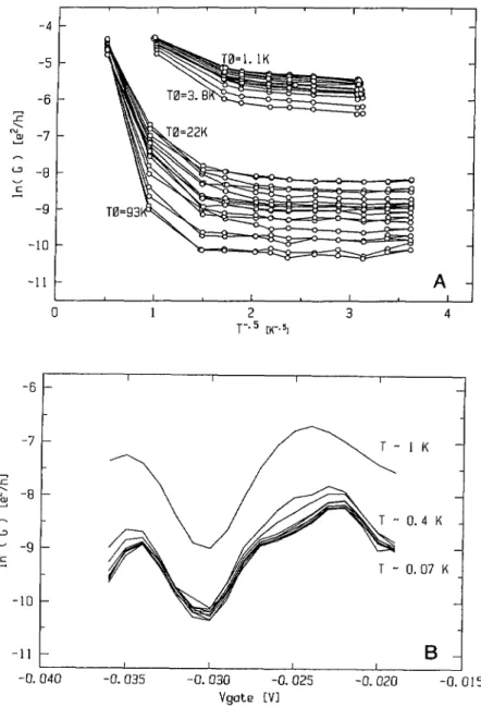
0 2 3 4 T~.~ iK-.51 -6 -7 ~ ~ ~ -9 T -lo i 0. 035 Ygatg lvlFig.
4.A)
In(g) (in
quantumunits)
versusT~~/~
for various VG. The To parameter values for theextremal curves are indicated.
B)
In(g)
versus VG at various temperatures between T m I K andT ci 70 mK. The range of VG
corresponds
to the curves at the bottom offigure
4a.sample,
allowing
us to consideronly
atypical
resistor(ro,Eo)
given
by
Mott's law(see
Eqs.
(1-3))
in order to calculate the resistance of the wholesample.
But in IDwires,
such anaveraging
does not takeplace:
sinceelementary
resistors arealways
added inseries,
one hasto consider the
strongest
one(and
not the meanone)
in order to evaluate the resistance of thewire.
Such an idea can be
quantitatively
developed.
We now summarize what comes out of adetailed
analysis
of the Mott VRH in ID wires[5,6,15].
Let us consider along
wire withoutfluctuations of
quantum
origin
which allows us to useequation
(4)
for eachelementary
re-sistance
R,j
dud toget
their values as soon as the distribution(z~,E~)
of localized states is known. Onestatistically
neglects
resonant or directtunnelling
since we assume L » ro.Using
an
assumption
of localoptimisation
(at
eachstep
the electron chooses the less resistivehop),
one can selfconsistently
solve theproblem
of IDhopping
[15].
Due to apossible
local lack oflevels near the chemical
potentiel
~J,lengths
ofelementary
hops
fluctuate around ro,giving
forRq
a distribution whose width wq is solarge
that the addition of N =L/ro
resistancesRq
in series does notself-average (as
long
as N is notextremely
large).
Note that such a methodis consistent
only
if wq » wq, where wq is the width of the distribution of resistances due toquantum
interferences(wq
can beregarded
as the fluctuation of IIf
in(I)).
One can show
that,
if N < N* =~e~l~~f~~
(a
ci2),
the resistance of a wire isentirely
a
dominated
by only
oneelementary
most resistivehop:
Rmax
=
MaXN(Rq)
whose averagevalue is size
dependent.
Estimation ofRmax
gives:
In R ci In
Rmax
" ~~~~(8)
(
with < rmax >=2ro
@@
=((
~
)~/~
@@
(8bis)
TNote that in average over
disorder,
one still has aT~~/~
law. The measured In R doesnot
directly
give
To
but features of the dominanthop.
NeverthelessTo
theimportant
averaged
microscopic
energy can be estimated for ourexperimental
parameter
In R andfor reasonable
(:
in thecompanion
paper[15]
a simulation of our wire for In R ci +9 atT
= 0.45 K is
presented
with:(
= 21 ci 50 nm andTo
" 6 K(see
the comments in[15]
on theslight
discrepancy
between calculated and measured InR).
(
ciI,
so we call thisregime
"strongly
localized",
by
contrast with the"barely insulating regime"
that one encounters nearM-I-T- where
To
is notlarge enough
compared
to T to allow adescription
in terms of variable rangehopping.
In thisregime
(
must begiven
in order ofmagnitude by
L~
ci 130 nm(at
verylow
temperatures),
I-e-(
» I.Moreover,
we foundnumerically
that the wholeexperimental
range of conductancescor-responds
to variations ofTo
between 2 K and 10 K. Let usemphasize
that these values aresignificantly
lower than thosenaively
extracted from data inT~~/~
scale(see Fig.
4a)
which,
as we
explained,
isdefinitely
not relevant for agiven
wire in Mott'sregime.
Nevertheless,
asalready
pointed,
noprecise
determination of thetemperature
exponent
can be extracted fromthe
experiment,
and the choice of the abscissa infigure
4a is ratherarbitrary.
1. 5 SATURATION OF THE CONDUCTANCE AT LOW TEMPERATURE. As noted
before,
thetemperature
dependence
of the conductance exhibits a saturation below atemperature
whichincreases when the
gate
voltage
decreases. Because all the measured conductanceproperties
become
temperature
independent,
it islikely
to incriminate electronheating
by
radiofrequency
voltage
sources(let
us recall that the conductance is recorded in the I V linearregime).
Voltage
radiofrequency
noise is apriori
more efficient to heat electrons when conductanceis
high.
However the conductance saturation is clearonly
when conductance is low(small
VG).
Moreover the saturationtemperature
is the same for thepeaks
and thevalleys
of theconductance
pattern
even forpeak-to-valley
ratio aslarge
as10~,
in thestrongly
localizedEven if it is difficult to rule out
heating by radiofrequency
pickup,
the observed saturation up to T= 400 mK seen in the
strongly
localizedregime
could be due to intrinsicphysical
effects: either resonanttunnelling
processes or the existence ofplateaus
in thetemperature
dependence
of amesoscopic
ID wire in thehopping regime
[15].
A crossover from
hopping
athigh
temperatures
toT-independent
tunnelling
at lowtemper-atures should
happen
if thediverging
Motthopping length
To(more
precisely
rmax)
becomes of the order of thesample
length
at low T[2,19].
But the estimate of rmax ci 600 nmob-tained from the
reported
estimate ofTo
is about 10 times smaller than oursample
length
when the saturation of g occurs. The resonant
tunnelling
through
thesample
isnegligible
under this condition. Another observation
against
the resonanttunnelling
picture
is that the measured conductance isalways
decreasing
when thetemperature
decreases,
even forsharp
conductance
peaks.
However it is well known that inelastic processesalways
decrease theres-onant conductance in the
tunnell1~lg
processes, whereasphonons always
increase thehopping
conductance. For these reasons we do not believe that resonant or directtunnelling
processesare of
importance
in ourgeometry.
Apart
from resonanttunnelling
orheating,
special
features oftemperature
dependence
inID V.R.H. could
give
rise totemperature
saturation. Asreported
infigure
2 of[15],
one has
to
distinguish
two main cases for the temperaturedependence.
First,
when the temperatureis such that values of N
=
L/ro
arelarge enough
(precisely
when N > N* definedabove),
In R should vary as IIT.
Since To diminishes as Tincreases,
such aregime only
arises atquite
high
temperatures,
let us say: T > T*. T* isgiven by:
T* =~~
[15]
roughly
i~
~@
T*f
/~
proportional
toTo,
such that T* increases when thesample
becomes moreinsulating.
Asalready
noted,
one can indeed see infigure
4a and this is ageneral
trend that activatedbehavior is valid above a
temperature
which grows as thesample
is driven to a moreinsulating
regime.
Weestimate,
using
the definition of N* with theexperimental
parameters,
that: T* ci 1 2 K in thestrongly
insulating
regime.
What
happens
if N < N*? As discussed in[15]
we think that in this case theactiva-tion energy of the dominant link can be very
weak,
leading
to anapparent
saturation of Rwith
decreasing
T. If thishappens,
such a non-activated link will remain dominant aslong
as the second-dominant activated link becomes more resistive because of
decreasing
T. ThusT-dependence
of R will be a succession of "activatedsegment
apparent
plateau"
and reference[15]
shows that in alogarithmic
scale of Tplateaus
andsegments
are of same size. Whenaver-aging
over manysamples,
one should however recover Mott's ID law due to random locationof
segments
andplateaus
for differentsamples.
However,
the observed saturation of R islarger
than the size ofplateaus
predicted
in[15]
and moreover we never see an activated
segment
attemperatures
lower than the temperatureat which saturation
begins.
Therefore,
we think thatheating
by
rfpick-up
could bepartly
responsible
for the observed saturation.Up
to now, thestudy
of thetemperature
dependence
in the localisedregime
has been carriedout without
taking
into account anyquantum
fluctuations. We now focus on conductancefluctuations versus Fermi energy and on the effect of
magnetic field,
which willgive
us much moreinsight
into the relevance of zerotemperature
theories for ourexperiment.
2. Conductance fluctuations in the localized
regime.
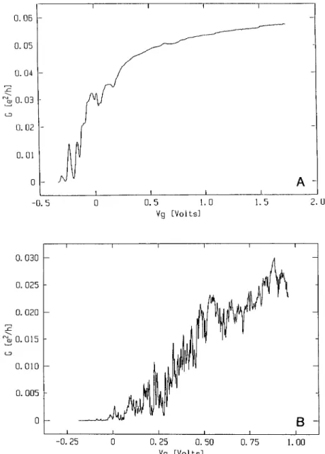
o. off o. 05 o. oi 2
~
0. 03 co 0. 02 o. o1 0A
-0. 5 0 0. 5 1. 0 1. 5 2. Vg lvol Lsl 0. 030 0.025 0. 020 Iio.ois
co o. oio o. oos 0 £~ -0. 25 0 0. 25 0. 50 0. 75 1. 00 Yg lYolLsiFig.
5.A)
Conductance in quantum units versus the gatevoltage
at T= 4.2 K.
B)
The same atT
= 100 mK.
two
temperatures:
T= 4.2 K and T = 100 mK
(a
thermalcycling
up to roomtemperature
has beenapplied
between the tworecords).
The relative fluctuation becomes enormous for smallvalues of the conductance
(sometimes
exceeding
two orders ofmagnitude),
so that asemilog
representation
is moreadapted
(Fig. 6).
2. I
QUANTITATIVE
ANALYSIS OF THE LOG-NORMAL CONDUCTANCEFLUCTUATIqNS.
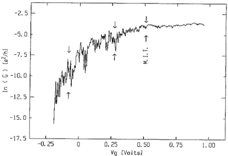
In-2. 5
1
~~'~i
i
w fi -7. 5~
= $ ~ co o. o ~ -12. 5I
-15. o -17. 5 -0. 25 0 0. 25 0. 50 0. 75 1. 00 Yg lYo LslFig.
6.Figure
58 ina
semi-logarithmic
plot.
The arrows indicate the estimated Anderson transitionand the
barely
andstrongly
insulating regimes
where themagnetic
fielddependence
has beenprecisely
studied
(see
Fig.
8).
based on the considerations
developed
successively by
Lee [5], Raikh and Ruzin[6],
and Ladieu and Bouchaud[15].
Figure
7 shows61n(R)
versus <In(R)
> for T = 100 mK and H = 0 T. <ln(R)
> is obtainedby
numericalsmoothing
ofIn(R)
to remove the shortVG-range
fluctuations. Twoexperiments
differing only by
a thermalcycling
to roomtemperature
arepresented
in order toimprove
the statistics.As we
reported
in thepreceding
section,
the measured In R is dominatedby
the mostresistive link
Rmax
whose value is sizedependent.
Thusamplitude
of fluctuations isgiven
by
the width wN of
Rmax
distribution. Estimation of wN leads to wN < w~j, andgives:
In R
21n(aN)
~~~Fortunately,
thisprediction
depends weakly
on thesingle adjustable
parameter
N,
for real-isticlarge
values of N. Wenumerically
found(see Fig.
4 of[15])
that N ci53,
but eventaking
N
= 25 100 (To " 50 200
nm),
weget
a smalldispersion:
~~~ ~
= o-II + .ols
(lo)
This
prediction
isreported
infigure
7,
in verygood
accordance with theexperimental
data.Therefore,
at thispoint,
one does not need to invoke thequantum
coherence toexplain
theobserved
amplitude
of61n(R).
We now detail thearguments
whichjustify
the introduction ofquantum
fluctuations within the most resistivehop.
3 2 i $ * cc
~
~ 0 -1 -2 ' 0 2. 5 5. 0 7. 5 10. 0 12. 5 15. 0 < Lnl R*g~/h >Fig.
7.61n(R)
versus < In R > in quantum units at T = 100 mK. Two experiments arerepresented
to
improve
the statistics. < ln g > is obtained aftersmoothing
of theexperimental
curvesg(VG).
Dotted lines are the
prediction
of reference [15]. Note nevertheless thetendency
of 61n R to saturate at ci I forhigh
resistances.typically
in ourstrongly
localizedregime (for
T ci 0.5K).
This energy scale is in fact twice themean energy
spacing
of levelslying
within rmax.However,
numerical simulations ofquantum
fluctuations versus Fermi energy at T = 0 K have been carried out very
recently
[20]
companion
paper).
They
havesuggested
that thetypical
width in energyAEqu
of these fluctuations is of the order of the mean energy levelspacing
within the finitequantum
coherentsystem.
Letus assume, as
usual,
that quantum coherence ispreserved
on the scale of eachhop
at finitetemperature.
Then,
weget
thatquantum
interferences in the dominant linkchange
completely
within a scale in energy
given by
the mean levelspacing
within rmax at finitetemperature.
Therefore,
weget
AEqu
ciAEg~o
at finitetemperature.
Crudely
speaking,
this means thatwithin rmax
quantum
interferences are dominatedby
diffusion on levels whose energy is theclosest to initial and final
energies
ofhop.
This energy issimply
ciAEg~o.
Of course, the latter statement is concerned with
only
mean energy scales.Therefore,
we think that observed fluctuations arepartly
of quantumorigin,
depending
on eachparticular
fluctuation: if for a
given hop,
quantum interferenceschange
with energy faster thangeomet-rical
fluctuations,
then the fluctuation will be ofquantum
origin
and therefore Tindependent.
If the inverse situation takesplace
we willget
astrongly
Tdependent
fluctuationjust given
by
geometrical
considerations.Indeed,
even for agiven hop,
providing
that the value of theresistance is
given exclusively by
equation
(4),
the fluctuation inducedby
varying
Fermi energy is very sensitive to any shift oftemperature.
Figure
4bgives
anexample
of a fluctuation ofquantum
origin.
Indeed,
one can see thatthis conductance fluctuation 61n g exhibits no or a very weak
temperature
dependence,
evenin a temperature range where the mean conductance
keeps
ondecreasing
withdecreasing
T(here,
e-g- between T = I K and T = 400mK).
Thisbehavior
suggests
that finitetemperature
models
totally
removing
quantum
interferences areincomplete.
worth
noting
that the zerotemperature
RMT or FDPapproaches
predict:
Aln R ci~
>
T
~
l
(see
[15],
o =1/4
or1/10
for R-M-T- and F.D.P.respectively),
whereas thegeometrical
oneis
always
£
I in ourexperiment.
Thisquantitative
analysis
shows that the fluctuation that we observe cannot be the fullquantum
one, but is truncatedby
thegeometrical
fluctuation. Thismeans that when a
quantum
fluctuation inside thelargest
(dominating)
resistoryields
alarge
increase of the
resistance,
the electronshop
to a different finalimpurity
site. On thecontrary,
when a
quantum
fluctuationyields
alarge
decrease of theresistance,
the secondlargest
resistorstarts
playing
aleading role,
thereforelimiting again
the fluctuation of measured In R.Near the Anderson
transition,
wq is nolonger
muchlarger
than the estimatedquantum
fluctuations
ii
5],
which means that the above considerations breakdown since the method used is nolonger
valid.Physically,
this means that the effect of interferences within(
itself can nolonger
beignored
(quantum
fluctuations can beregarded
as fluctuationsoff).
Moreoverbecause wq
decreases,
the whole conductance is less and less controlledby
the weakest link. In thisregime,
thequantum
fluctuation shoulddevelop fully,
but this range is too narrow toallow a
quantitative
test.Moreover,
thetemperature
dependence
of fluctuations in thisregime
is much more marked than in theregime
offigure
4b. Thisemphasizes
that thedescription
of thevicinity
of the transitionrequires
a model where quantum fluctuations arefully
taken intoaccount,
and notonly
considered on the dominant link.The
study
of fluctuations versus the Fermi energy shows the subtleinterplay
between quan-tum andgeometrical
fluctuations. Theapplication
of amagnetic
field can induce Zeemanshifts of energy levels
E~
in(4),
andconsequently
inducegeometrical
fluctuations. On the other handmagnetic
flux canchange
thequantum
interferences and inducequantum
fluctua-tions. We will see in the next section thatmagnetoconductance
fluctuations arepurely
due toquantum
interference effect in oursample.
2. 2 THE FLUCTUATIONS IN APPLIED MAGNETIC FIELD VERSUS THE FLUCTUATIONS IN
VG.
Figure
8presents
a detail of the conductance fluctuation versusgate
voltage
andapplied
magnetic
field for both very low andmoderately
low conductances at T= 100 mK
(see
Fig.
6).
2. 2. I
Strongly
localizedregime:
nonergodicity
For the very low conductances in a linearscale
representation
(Fig. 8A),
conductancepeaks
seem to appearjust by
application
of themagnetic
field,
as in reference [2]. In alogarithmic
representation
(Fig. 88),
however,
such conductancepeaks
correspond
to maxima of the conductance in zero field.Moreover,
theapplied
magnetic
field is unable to decorrelate thepattern
of the conductance fluctuationsversus the
gate
voltage.
This situation isprecisely
referred to asnon-ergodic
[3].
With thedata of
figure
88 we find indeed:var(In R)H
ci 0.22 <var(In R)v~
~ l.10This is not,
strictly
speaking,
aproof
that there isnon-ergodicity
in thisstrongly
localizedsituation because one first has to know if the field scale
appearing
in theproblem
is not toolarge
or,equivalently,
if the statistics over themagnetic
field iscomplete.
Ourexperimental
field range is limited below 4 or 5 T because of the
large negative
meanmagnetoconductance
associated with the
shrinking
of atomic orbitals forhigher
field [2Ii.
In fact when the condition: H »~
j
Cf 3 T
(for
a = aBohr and = 20 nm, the distance betweenSilicon
impurities)
ise a
satisfied,
themagnetic
field modifies theshape
of each wavefunction,
and notonly
thephase
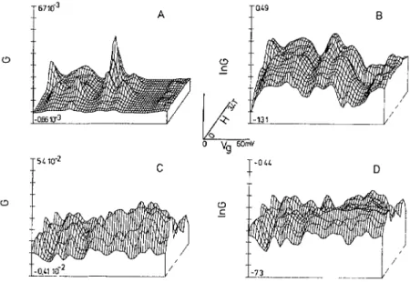
A B ~ ~ c
II
if ,/ ~ Q ° Vg 6°~~ C '~~~ D / /Fig.
8. Conductance as a function of VG and H in a 3D-Plot. The VG ranges are indicated infigure
6.
A)
Low Conductances in a linear scale.B)
Low Conductances in alogarithmic
scale.C)
Moderateconductances in a linear scale.
D)
Moderate Conductances in alogarithmic
scale.Between 0 and 3A
T,
typically
weonly
see 2 or 3 oscillations ofIn(g(H))
in thestrongly
localized
regime.
The correlation field(difficult
to beestimated)
is of order I T(a
quantum
of flux
hle
isput
through (64 nm)~
for IT).
Nevertheless,
thecomparison
with thebarely
localized situation shows that theexperiment
distinguishes,
inpractice,
theergodic
andnon-ergodic
cases even for one or two oscillations ofmagnetoconductance.
The observed
non-ergodicity
implies
that themagnetic
field is unable to inducegeometrical
fluctuations. On the contrary, a
strong
Zeeman shift wouldchange
all theimpurity
energies
and thus the
geometry
ofhopping
paths
[2-3]
inducing geometrical
fluctuations. We do not seethe
magnetic
fieldtranslating
the maxima of In g[2],
and so Zeeman effects arenegligible
in oursample
for our field range.The
experiment
shows that thequantum
fluctuation versusmagnetic
field(AIn
RH
<I),
issmaller than the
geometrical
fluctuation(AIn
Rg~o
ciI).
This is in thespirit
of theNguyen,
Spivak
and Shklovskii model [8], where thequantum
fluctuation versusmagnetic
flux is smallerthan any other kind of fluctuation. This has been
already
noticedby
Orlov et al. in reference[3].
Furthermore we havesuggested
in section 2.I that thegeometrical
fluctuation is smallerthan the
quantum
fluctuation versus energy(AIn
Rqu
>I)
"truncatedquantum
fluctuation").
This allows us to conclude that the quantum fluctuation is
larger
versus energy than versusmagnetic
field. To ourknowledge,
there is no attempt to model the fluctuation versus energy at T= 0 K
apart
from that of Avishai and Pichard[20].
In thestrongly
localizedregime,
theirnumerical results show a similar
non-ergodic
behavior,
precisely
when standard RMT resultsstart to fail.
2.2.2
Barely
localizedregime:
ergodicity
Figures
8C and 8D show the conductance as a function of VG andapplied
magnetic
field at T= 70 mK for a range of conductance
just
on theinsulating
side of the Anderson transition:typically
<In(g(H
=0))
>+~-5(g
+~ 7 x10~3),
o A
vgimvl
~°
o B
vglmvl
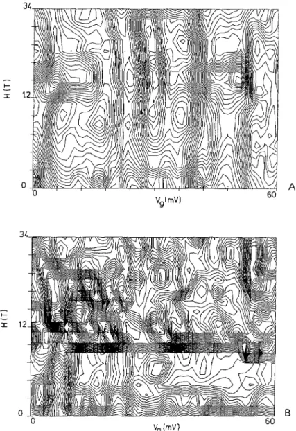
~~Fig.
9. Contourplots
offigures
8b and 8d. Themagnetic
field does not decorrelate the conductance pattern versus gatevoltage
in thestrongly
localizedregime
(9A).
On the contrary the situation isergodic
in thebarely
localizedregime
(98).
conductances,
To
~ 2K,
so that we are in thelimiting
case of the VRHregime.
In this rangeof
conductance,
theshape
of the fluctuations is reminiscent of what is observed moredeeply
in the
insulating
regime.
By
contrast to thestrongly
insulating
regime,
near the Andersontransition,
theexperiment
indicates the
validity
of theergodic
hypothesis
formulated first in the diffusiveregime
for small disorderparameter
(kfl)~~
var(In R)H
Cf 0.19 Cfvar(In R)v~
t 0,27in the critical
insulating
regime.
We have seen that near the Anderson transition it is nolonger
relevant toseparate
geometrical
andquantum
fluctuations: theanalysis
performed
in thestrongly
localizedregime
fails asalready
mentioned in section 2.I.Because the estimated
(
becomesquite
large
withrespect
to the distance betweenimpurities,
the electrons are nolonger
fixed to agiven
impurity
but localized in shallowregions,
which arechanged by
theapplication
of amagnetic
field. Because of thisredistribution,
theergodic
hypothesis
is realistic. It is indeednumerically
obtainedby
Avishai and Pichard near the Anderson transition[20].
But as we mentioned in
2.I,
the extension of this criticalregime
((
»I)
in our MBE grown GaAs:Sisample
appears to bequite
narrow. We believe that it is much moredeveloped
inless pure
samples
likeamorphous
alloys.
Because of this narrowness, it is difficult to be morequantitative.
In both NSS model and RMT
model,
there exists a close connection between thequantum
fluctuations and the
averaged
magnetoconductance
effect;
let us now turn to theanalysis
ofthe mean
magnetoconductance
effect.2.3 THE MEAN MAGNETOCONDUCTANCE EFFECT. Positive
magnetoconductance
at lowtemperatures
ininsulating
GaAs:Si wasreported
long
ago[3, 13,
22].
Amongst
the modelswhich have been
proposed,
Spivak
and Shklovskii[8, 21]
predict
at themacroscopic
limit,
that:In
(°~~
~~~~
ci 1(12)
(Hc
isgiven by
~(~~
),
which compares very well with numerical simulations[8].
~o
(l/2~
Zhao et al.
[10]
argue that simulationsperformed
within the same framework of FDPanalysis
but onlarger
samples,
show no saturation of themagnetoconductance
in the limit of verylarge
quantum coherentsample
(I.e.
very lowtemperatures).
Moreoverthey give
auniversal estimate:
in
i~ll
~ o-ii
WhereLH
-l~
HI
~~~(13)
Their simulations corroborate the results obtained
by
Medina et al.ill].
As noted in the
introduction,
RMTpredictions
differ from the FDP model because thepositive
magnetoconductance
(in
case ofnegligible
spin-orbit
scattering) depends
onroll
andnot
only
on To(the
predictions
differcompletely
in the case ofstrong
spin-orbit
scattering).
For instance at T
= 0 K
(to
avoid the introduction of thephase
coherenthop
and itsmagnetic
fielddependence)
~~~~~~10~~~
'~((H~
Hc)
~~0)
2~0)
~~~~~~~~
~~~~if
((H
>Hi)
=2((0)
[12]
(quasi
ID RMTresult;
Hi
isgiven
by
H](~
ci)~).
At finitetemperature,
theexpression
is lesssimple
because Todepends
weakly
on H via((H)
[12].
Nevertheless,
the meanmagnetoconductance
is very sensitive to the mean conductance in zerofield in this RMT
approach.
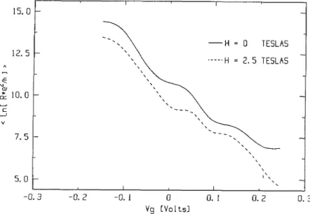
Figure
10 shows the meanmagnetoconductance
effect between H = 0 and H = 2.5 T in the15, o
~",,
-H 0 iE5LA5 ~ ~~'~,,~~
.---.H 2. 5 TESLAS°~
"',,
(10. 0 ,, t"---,
$
",,
7.5~~',,~~~~
5.0~",,
-0. 3 -0. 2 -0. 0 0. 0. 2 0. 3 Yg lYoltsiFig.
10. The smoothed conductance for H= 0 and H = 2.5 T in the
strongly
localizedregime.
Theobserved mean
magnetoconductance
effect isroughly
insensitive to the conductance value(at
H=
0)
g(H
= 2.5
T)
and fluctuates around:
In(
~W I, the meanmagnetoconductance
value afteraveraging
g(H
=0)
over the whole range of VG.
conductance after numerical
averaging
of the fluctuations in VG varies over 3 orders ofmagnitude.
Nevertheless < In~~~
~'~~~
> is
roughly
unchanged
andapproximately
9(°)
equal
to I. Theaveraging
over the whole range VGgives
In~~~'~
~~
ci I. This is
just
the9(°)
prediction
of NSS[8-21]
(the averaging
needed for thisprediction
is obtainedby
smoothing
in VG which extends over severalfluctuations).
We note that it is also ingood
accordance withthe result of Zhao et al.
ii
Ii
if we suppose that To ~ 160 nm, a realistic value in ourexperiment,
is
roughly
insensitive to <g(0)
>. However we are not able to test theiranalytical
universalresult. In any case, the
insensitivity
of the meanmagnetoconductance
to the mean conductancevalue stresses the fact that FDP
approaches
are moreadapted
than RMTapproaches
in thisregime.
As one
approaches
the Andersontransition,
the meanmagnetoconductance
tendssmoothly
to the weak antilocalization contribution in the diffusive
regime.
Contrarily
to thestrongly
insulating
regime
where the meanmagnetoconductance
and the conductance fluctuations are of the same order ofmagnitude,
near the transition the meanmagnetoconductance
becomesmucll
larger
than the fluctuations. Theanalysis
in thebarely
localizedregime
in terms ofchanges
of the localizationlength
is restricted because of the small range of conductance where thisregime
occurs. Nevertheless the observedmagnetoconductance
iscompatible
with a small increase of(
(for
instance((2.5 T)
=1.3((0)
for To Cf 2K),
aspredicted
by
RMTapproach
[9]:
(
=