HAL Id: hal-03137102
https://hal.uca.fr/hal-03137102
Submitted on 10 Feb 2021
HAL is a multi-disciplinary open access archive for the deposit and dissemination of sci-entific research documents, whether they are pub-lished or not. The documents may come from teaching and research institutions in France or abroad, or from public or private research centers.
L’archive ouverte pluridisciplinaire HAL, est destinée au dépôt et à la diffusion de documents scientifiques de niveau recherche, publiés ou non, émanant des établissements d’enseignement et de recherche français ou étrangers, des laboratoires publics ou privés.
Long catalyst-free InAs nanowires grown on silicon by
HVPE
Gabin Grégoire, Evelyne Gil, Mohammed Zeghouane, Catherine Bougerol,
Hadi Hijazi, Dominique Castelluci, Vladimir Dubrovskii, Agnès Trassoudaine,
Nebile Isik Goktas, Ray Lapierre, et al.
To cite this version:
Gabin Grégoire, Evelyne Gil, Mohammed Zeghouane, Catherine Bougerol, Hadi Hijazi, et al.. Long catalyst-free InAs nanowires grown on silicon by HVPE. CrystEngComm, Royal Society of Chemistry, 2021, 23 (2), pp.378-384. �10.1039/d0ce01385d�. �hal-03137102�
Long catalyst-free InAs nanowires grown on silicon by HVPE
Gabin Grégoire1, Evelyne Gil1,4, Mohammed Zeghouane1, Catherine Bougerol2, Hadi Hijazi4, Dominique Castelluci1, Vladimir G. Dubrovskii5, Agnès Trassoudaine1, Nebile Isik Goktas3,
Ray R. LaPierre3, Yamina André1,3,4
1UniversitéClermont Auvergne, CNRS, SIGMA Clermont, Institut Pascal, F-63000 Clermont-Ferrand, France
2Université Grenoble Alpes, CNRS, Institut Neel, 38000 Grenoble France
3Department of Engineering Physics, McMaster University, Hamilton, Ontario Canada, L8S4L7
4ITMO University, Kronverkskiy pr. 49, 197101 St. Petersburg, Russia
5St. Petersburg State University, Universitetskaya Emb. 13B, 199034, St. Petersburg, Russia
Abstract
We report for the first time on the hydride vapor phase epitaxy (HVPE) growth of long (26 µm) InAs nanowires on Si(111) substrate grown at a standard rate of 50 µm/h. The nanowires grow vertically along the (111)B direction and exhibit a well faceted hexagonal shape with a constant diameter. The effect of the experimental parameters, growth temperature and III/V ratio, is investigated. The thermodynamic and kinetic mechanisms involved during the growth of such long nanowires are identified. It is demonstrated that growth occurs through direct condensation of InCl and As4/As2 gaseous species. Dechlorination of adsorbed InCl molecules is the limiting
step at low temperature. Structural analysis through high resolution transmission electron microscopy (HRTEM) and high-angle annular dark-field (HAADF) imaging was performed. The high As4 partial pressure of the HVPE environment induces the presence of both wurtzite
and zinc-blende phases. The results emphasize the potential of the low cost HVPE technique for the monolithic integration of arrays of long InAs nanowires on silicon.
1. Introduction
Growth of III-V semiconductors on silicon is still a topical subject due to the promise of inexpensive and highly efficient electronic and optoelectronic device integration. In particular, InAs has attracted special attention due to its direct and narrow band gap, high electron mobility and small electron effective mass.1 Consequently, the integration of InAs with Si generates a
great deal of interest for ultra-high speed and low-power components.2,3 However, the planar
hetero-epitaxy of high quality InAs materials on silicon remains a difficult task due to the large difference in the lattice constant between InAs and Si.4 The large epitaxial strain leads to surface
roughness and high dislocation densities, which inhibit any relevant electrical and optical properties expected from InAs material.
Unlike planar thin films, nanowires (NWs) address the issue of the large InAs/Si lattice mismatch (11.4 %).5 The NW geometry allows an efficient elastic stress relaxation through the
free lateral surfaces, enabling the growth of free-standing III-V materials even in high lattice-mismatched systems.6 The performance of chemical or biological sensors, infrared
photodetectors7,8 and solar cells 9 are expected to be improved through the specific properties
of NWs.
The growth of InAs NWs on silicon has been demonstrated by molecular beam epitaxy (MBE) and metal-organic vapor phase epitaxy (MOVPE), involving predominantly Au-catalysed, Ag-catalysed and self-Ag-catalysed vapor-liquid-solid (VLS) growth.10–15 The ultra-clean environment
and the low growth rate of MBE enable the growth of very thin and pure defect-free InAs NWs using Ag or Au particles.14,16 However, a foreign metallic catalyst particle is known to act as an
impurity by introducing deep level recombination centers, which significantly degrade the electrical and optical properties of the system.17 For self-catalysed InAs NWs, the indium
catalyst is obtained either by in-situ deposition prior to growth 18 or by initiating growth under
indium-rich conditions.19 In either case, the NW morphology is very sensitive to the growth
parameters such as the growth temperature and the vapor phase composition,20 and structural
defects in the InAs crystal such as twin planes and stacking faults are always reported.19,21
Significant efforts aimed to develop catalyst-free InAs NWs have been made by MBE and MOVPE. NWs grown by MOVPE generally exhibit higher growth rate due to higher material input and growth temperature compared to MBE.22,23 However, for both techniques the authors
show that vapor-solid (VS) growth of InAs NWs is mainly limited by surface diffusion of adatoms23–25, also exhibiting a high density of twin planes and stacking faults.11,22,26
Hydride vapor phase epitaxy (HVPE) has shown exceptional results for both Au-catalysed and self-catalysed ultra-long GaAs NWs in terms of growth rate and crystalline quality without any polytypism regardless of NW diameter.27,28 This is due to the use of chloride (GaCl) precursor
in the HVPE process, together with hydride V-H3, which induce specific growth mechanisms.
No studies have been conducted thus far to grow InAs NWs by this technique. We report here on the growth of catalyst-free vertically aligned InAs NWs on silicon (111) substrate by HVPE. An experimental study as a function of growth parameters is carried out to reveal the steps and mechanisms involved in the growth of the NWs. The observed experimental trends are supported by kinetic and thermodynamic considerations developed for III-V semiconductors grown in the HVPE environment.
2. Experimental
Prior to growth, Si(111) substrates were etched with hydrofluoric (HF) acid to remove the native oxide, then rinsed in deionised water and finally blow dried with N2. These substrates
were then introduced in a custom HVPE reactor working at atmospheric pressure with H2 as
carrier gas. The reactor is divided into three zones, heated by a six-zone furnace. In the source zone, indium chloride (InCl) gaseous species are produced by reacting HCl gas with liquid indium at 700 °C. HVPE is a hot wall reactor technique, needed for producing the InCl precursors and insuring their stability downstream to the substrate. Arsine gas (AsH3) is
introduced in the downstream central zone of the reactor heated at higher temperature, to ensure a homogeneous mixing of the gas phase and reduce parasitic nucleation upstream of the substrate, since the reactions involving chloride molecules are exothermic. AsH3 is totally
decomposed into As4/As2 species when introduced into the hot-wall reactor. One of the specific
attributes of HVPE is that the substrate surface interacts with a complex vapor composed of InCl, HCl, H2 and As4/As2, with the last two species being considered at equilibrium. The
substrate is placed in a downstream growth zone that is kept at lower temperature than the central zone. The partial pressures of InCl, HCl, As4 and As2 (H2 is 1 atm) above the substrate
are calculated as a function of the input flows (in sccm) of AsH3, HCl (above the liquid In
source) and H2, the kinetics of decomposition of gaseous AsH3 into As4 and As2,29 and the
thermodynamic equilibrium constants of intermediate chemical reactions, by taking into account the temperature gradient along the reactor. In the following, we will discuss results as a function of the III/V ratio, calculated as the ratio between the partial pressure of gaseous InCl over the partial pressure of gaseous As4 interacting with the substrate surface in the growth
of As4 is a hundred times greater than the As2 partial pressure. The growth time was fixed to 30
min.
The morphology of the as-grown InAs NWs was studied using a Carl Zeiss Supra scanning electron microscope (SEM) with an acceleration voltage of 3 kV. The crystalline quality of the InAs NWs was investigated by high resolution transmission electron microscopy (HRTEM) and high-angle annular dark-field (HAADF) imaging using a FEI-Tecnai microscope operated at 200 kV and a Titan 80-300 HB scanning TEM (STEM) with double aberration correction. The latter instrument achieves sub-Ångstrom resolution both for phase contrast imaging and STEM.
3. Results and discussion
The effect of the growth temperature on InAs NWs growth is presented first. The partial pressures of As4 and InCl were fixed at 3.6 x 10⁻⁴ atm and 6.4 x 10⁻³ atm above the substrate
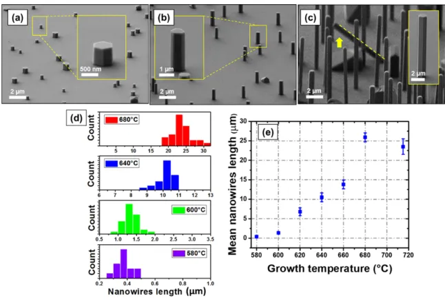
respectively, giving a III/V ratio of 18. Figures 1 (a)-(c) show tilted-view SEM images of the samples grown at different growth temperatures of 580 °C, 600 °C and 640 °C, respectively. InAs NWs grow predominantly along the vertical [111] direction whatever the growth temperature. Some tilted NWs with respect to the substrate were observed as highlighted by the arrow in Figure 1 (c). Tomioka et al. 30 demonstrated the important role of the surface treatment
prior to III-V NW growth on Si(111). They showed that III-V NWs grow along only one (111)B direction on As-terminated Si(111), whereas NWs can be grown along three equivalent (111)B directions for Ga-terminated Si(111). In this work, no surface treatment was done prior to the growth step. Thus, the presence of vertical and a few tilted InAs NWs may be due to the non-polar nature of the Si(111) substrate.31
Figure 1: Tilted-view SEM images of InAs NWs grown on Si(111) substrate at different growth
temperatures: (a) 580 °C, (b) 600 °C and (c) 640 °C. Insets show a magnified view of a single NW. (d) Length distributions of InAs NWs for different growth temperatures. (e) Average NW growth rate as a function of the growth temperature.
Regardless of the growth temperature, the NWs clearly have a uniform diameter with a hexagonal shape delimited by six equivalent {11"0} side facets and (111)B facet at the top. The NWs did not exhibit any In metal droplet at the top, suggesting that the NWs grow by a catalyst-free mechanism. Similar findings on InAs morphology were observed in ref 23, where NWs were grown by a vapor-solid (VS) mechanism. The formation of metal liquid In particles that would initiate a VLS growth mode is thermodynamically unfavorable in the HVPE environment because it is difficult to form droplets of In from InCl gaseous precursors on the substrate surface. This is further described in the Supporting Information. Owing to the large lattice mismatch between Si and InAs (11.4%), and therefore the large interfacial energy, InAs thin film growth is prevented. Thus, growth is likely initiated with the formation of self-assembled InAs islands by the Volmer-Weber mode on the oxide-free surface. The one-dimensional form of NWs at growth temperatures above 600 °C is ensured by the growth conditions, which promote anisotropic growth where the axial growth rate is maintained higher than the lateral
one. HVPE was proven to be a very powerful growth technique for shaping 3D structures by taking advantage of the large intrinsic anisotropic growth of III-V material.32,33
The nucleation stage determines the island size and NW diameter. Nucleation strongly depends on the silicon surface, with a random surface re-oxidation occurring after HF etching prior to the introduction of the substrate into the reactor for growth. This likely explains the large dispersion in the NW diameter on the same sample. No dependence has been observed between length and diameter.
The variation of the axial growth rate of InAs NWs as a function of the growth temperature is presented in Figure 1(e). The growth rate was determined from statistical analysis as shown in Figure 1(d) and calculated by dividing the average length of the NWs by the growth time. It can be observed that the axial growth rate increased from 0.8 µm/h to 51.8 µm/h with increasing growth temperature from 580 °C to 680 °C. The axial growth rate decreased to 42 µm/h at a higher temperature of 715 °C. Similar dependence of the axial growth rate of InAs NWs with the growth temperature was observed by MBE and MOVPE 24,34 where growth was governed
by the thermally-activated adatom diffusion on the surface of the substrate and NW sidewalls.20,34 HVPE growth is mainly driven by the balance between adsorption and
desorption of precursor materials, and the kinetics of the dechlorination step. Surface diffusion of ad-species is not limiting in the HVPE process.35–37 A first simple analysis indicates that at
low temperature, growth is limited by decomposition of adsorbed precursors, e.g., dechlorination. As the temperature increases, the growth rate increases due to thermal activation of the dechlorination step until desorption prevails for the highest temperature, resulting in a maximum growth rate with temperature (Figure 1(e)).37
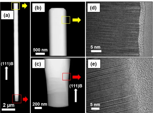
Structural characterization by HR-(S)TEM was carried out to examine the crystalline quality of the NWs. Figure 2(a), (b) and (c) show HAADF-STEM images of an InAs NW grown at 680 °C with a III/V ratio of 3. Energy dispersive x-ray spectroscopy, shown in the Supporting Information, confirmed that the NWs are InAs.
Figure 2: (a) HAADF of InAs NW, (b) NW top and (c) NW base. (d) and (e) Corresponding
HRTEM images of (b) and (c), respectively.
The uniform diameter and the well faceted top of the NW indicate that growth occurs through a direct condensation from the vapor phase. The reverse tapered base of the NWs is due to the transient regime during which the partial pressures of the gaseous precursors reach their equilibrium values. HRTEM images taken from the top (Figure 2(d)) and the base (Figure 2(e)) of the NW indicate that the NWs exhibit alternating zinc-blende (ZB) and wurtzite (WZ) segments. These observations have been confirmed on dozens of wires grown at different growth conditions of temperature and III/V ratio. Z. Liu et al. 38 have reported that the crystal
phase of InAs was determined by the growth temperature and the As4 composition in the vapor
phase. The authors assumed that the appearance of structural defects during InAs growth was linked to the 2×2 surface reconstruction of the (111)B top facet of the NW. This was supported by a theoretical model based on the nucleation probability of both wurtzite and cubic phases. Based on that model, the presence of both phases in HVPE-grown InAs NWs over the broad range of growth conditions used in our work can be related to the high partial pressure of As4
used in the HVPE process (some 10-4-10-3 atm) compared to other growth techniques. Obtaining
single phase InAs HVPE NWs with an improved crystalline quality, by adjusting the growth temperature and vapor composition, is a topic of future study.
To model the axial growth rate of the NWs, we consider that there is a direct condensation from the vapor phase onto the (111)B top surface of the InAs NWs.The growth of InAs NWs
proceeds through the following reactions, depicted in Figure 3, for axial growth perpendicular to the (111)B face: 2As2(g) ⇄ As4(g) (1) 4V+As4(g) ⇄ 4 As (2) As+InCl(g) ⇄ AsInCl (3) AsInCl+ &'H 2(g) ⇄ InAs(c)+HCl(g) (4)
where V is an In vacant site on the substrate surface; index g is assigned to gaseous molecules; index-free species are adsorbed molecules or atoms; and index c is for crystalline species. InAs deposition can be summarized by the global reaction:
1
4As4(g)+InCl(g)+ 1
2H2(g) ⇄ InAs(c)+HCl(g) (5)
Figure 3: Schematic of InAs nanowire growth. Step I - Volmer-Weber nucleation of a 3D
island. Step II - As adsorption on vacant In (reaction (2)), on which InCl molecules adsorb (reaction (3)), and chlorine desorption into HCl by H2 (reaction (4)). Step III – Axial growth
rate prevails. There is no diffusion of the precursors on the substrate surface, growth precursors do not incorporate on the NW sidewalls.
HVPE is described as a near-equilibrium process. One can understand it as reacting almost immediately upon an increase of the supersaturation of the vapor phase toward return to equilibrium, which produces the solid. On decreasing the supersaturation, for instance by the use of additional HCl in the vapor phase, reversible processes occur at the vapor-solid interface due to the volatility of the chlorides. It is therefore important to introduce a supersaturation of the vapor phase, γInAs, which represents the state of advancement of the growth reaction (5) with
respect to the equilibrium:
γ
InAs=
[As4]1/4[H2]1/2[InCl][HCl]×KInAseq
-1
(6)where [i] is the partial pressure of gaseous species i above the substrate and KInAseq is the equilibrium constant determined by calculating the Gibbs free energy difference between solid InAs and vapor composed of As4, InCl, HCl and H2. γInAs is plotted as a function of the growth
temperature in Figure 4 (a) (blue curve). It remains positive over the temperature range examined: the vapor is supersaturated with respect to the equilibrium vapor, and growth occurs. The supersaturation parameter decreases with increasing temperature, meaning the growth rate would continuously decrease, which is not observed. A complete model should also consider the kinetics of dechlorination, which is thermally activated. Thus, it is important to determine the dechlorination frequency (kinetics of reaction (4)), which is responsible for the low growth rate that is observed at low temperature, despite favorable thermodynamic conditions.
According to Eq. (4), AsInCl is the source for the InAs crystal units; the latter reacts reversibly with AsInCl. A complete general model describing growth of crystal units (here InAs) from source units (here AsInCl) has been reported for reversible and irreversible vapor phase epitaxy systems.36 The model takes into account adsorption and desorption of precursor materials
(reactions (2) and (3)), dechlorination frequency (reaction (4)) and diffusion of ad-species on the surface before being incorporated into the crystal. We suppose that the desorption frequency of InCl according to reaction (3) is much higher than the dechlorination frequency (see Supporting Information). In such a case, the growth rate of InAs can be reduced to the simple growth rate expression for direct condensation in a one-particle system, which can be expressed as a function of the surface coverage of vacant sites on the top facet θV:
where θV (the fraction of vacant surface sites) and k are detailed in the Supporting Information.
Figure 4: (a) Variations of the coverage of vacant surface sites and of the supersaturation as a
function of the growth temperature. (b) Variation of the axial growth rate as a function of the growth temperature at a III/V ratio of 18.
The red curve in Figure 4 (a) shows the variation of the surface coverage of vacant sites (V) as a function of the growth temperature. Figure 4 (b) shows the variation of the growth rate as a function of the temperature. At low temperature, growth is limited by dechlorination of InCl ad-molecules and desorption of species. The surface is then blocked with undecomposed AsInCl species. This explains the low surface coverage of vacant sites and the low growth rate even at high supersaturation. When the temperature increases, the dechlorination frequency increases. Consequently, θV starts to increase and the axial growth rate significantly increases
with the temperature up to a maximum of 680 °C (as seen in Figure 4 (b)). At high temperature of 715°C, desorption of InCl becomes predominant and the growth rate decreases.
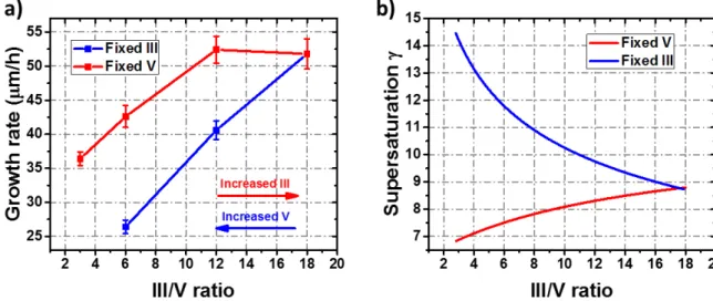
The effect of the III/V ratio on the axial growth rate has also been studied. SEM images of InAs NWs grown at different III/V ratios are shown in the Supporting Information. The growth temperature was fixed at 680 °C where the growth rate was greatest. The evolution of the average axial growth rate of NWs as a function of the partial pressures of both III and V elements is reported in Figure 5 (a). In Figure 5, either the InCl partial pressure was fixed at 6.4 x10⁻³ atm and As4 partial pressure was varied from 3.6 x 10⁻⁴ to 1.0 x 10⁻³ atm (blue curve), or
As4 was fixed at 3.6 x 10⁻⁴ atm and InCl partial pressure was varied from 1.0 x 10⁻³ to 6.4 x 10 -3 atm (red curve). This resulted in a III/V variation from 3 to 18. An increase of the InCl partial
rate saturated at higher III/V(as seen from the red curve in Figure 5 (a)). To explain this observation, we introduce thermodynamic and kinetic considerations as described earlier. At the growth temperature of 680 °C, the growth rate is assumed to be mainly dependent on the supersaturation since the growth temperature is high enough to ensure a fast dechlorination of InCl ad-species with respect to the incoming flux of material on the surface. As shown in Figure 5 (b), the supersaturation in the vapor phase, which promotes InAs deposition, increases with the input partial pressure of InCl. Consequently, the growth rate increases. When the III/V ratio is greater than 12, one observes a slight decrease of the growth rate, as the surface becomes blocked with a large amount of adsorbed InCl ad-species. The growth rate is then limited by the kinetics of dechlorination and remains nearly constant. This trend has already been studied theoretically and experimentally for the growth of GaAs by HVPE where the authors illustrated the surface blocking with the III-element as a function of the growth temperature and the partial pressure of GaCl precursor.39
Figure 5: (a) Variation of the growth rate as a function of the III/V ratio in the vapor phase.
(b) Variation of the supersaturation as a function of the III/V ratio.
The blue curve in Figure 5 (a) shows the variation of the axial growth rate as a function of the III/V ratio, by varying the partial pressure of As4 at a fixed partial pressure of InCl. The growth
rate increases from 26 µm/h to 52 µm/h when the III/V ratio increases from 6 to 18. Ref. 37 showed that the (111)B surface structure of III-As is sensitive to the growth temperature and the As flux in the vapor phase (AsH3, As4, As2), leading to different surface reconstructions
such as 1×1, 2×2 and √19×√19. Several studies have indicated that the 2×2 surface reconstruction originates from the formation of an As-trimer layer with very stable bonds under an As rich environment, which is obviously the case with the high material input of HVPE. As
a result, free dangling bonds for the incorporation of the III-element are missing and therefore the growth rate is reduced.40 On this basis, we assume that such a decrease in the growth rate
with As4 is related to the 2×2 surface reconstruction which corresponds to surface saturation
with the As-trimer bonds.
4. Conclusion
In this work, we demonstrate the direct growth of vertically aligned InAs NWs on silicon substrate by HVPE. The NWs grow along the (111)B direction with a constant diameter. The axial growth rate can be controlled with the growth temperature and the III/V ratio. The experimental results are supported by a simple theoretical model based on thermodynamics and surface kinetics. It is shown that the growth occurs through condensation and is mainly limited by the kinetics of decomposition of adsorbed species at low temperature and the thermodynamics of adsorption at high temperature. HRTEM characterization revealed the presence of both wurtzite and zinc-blende crystal structures in the NWs. This was attributed to the surface reconstruction of the (111)B surface at high As4 partial pressure in the HVPE
environment, which is responsible for the formation of such stacking faults and polytypism. Because growth is not limited by diffusion of adsorbed species from the substrate surface, HVPE is able to produce long NWs. As a matter of fact, our results highlight the potential of the HVPE process to grow well-aligned InAs NWs with a controlled growth rate on silicon substrate.
Author contributions
The manuscript was written through contributions of all authors. All authors have given approval to the final version of the manuscript.
Conflicts of interest
There are no conflicts of interest to declare.
Acknowledgement
This work was supported by Région Auvergne Rhône-Alpes; Pack ambition recherche; Convention n°17 011236 01- 61617. The authors thank 2MAtech, Aubiere, France, for scanning electron microscopy measurements. RRL and NIG are grateful for financial support from the Natural Sciences and Engineering Research Council of Canada. HH and VGD thank the Russian Science Foundation for financial support under the Grant 19-72-30004.
Corresponding authors
*Gabin GREGOIRE. Institut Pascal, 4 Avenue Blaise Pascal, 63178 Aubière Cedex. France. E-mail: [email protected]
*Yamina ANDRE. Institut Pascal, 4 Avenue Blaise Pascal, 63178 Aubière Cedex. France. E-mail: [email protected]
References
[1] N. Gupta, Y. Song, G. W. Holloway, U. Sinha, C. M. Haapamaki, R. R. LaPierre and J. Baugh, Nanotechnology, 2013, 24, 225202.
[2] K. Tomioka, M. Yoshimura and T. Fukui, Nano Lett., 2013, 13, 5822–5826.
[3] A. C. Ford, J. C. Ho, Y.-L. Chueh, Y.-C. Tseng, Z. Fan, J. Guo, J. Bokor and A. Javey,
Nano Lett., 2009, 9, 360–365.
[4] S. Gorji Ghalamestani, M. Berg, K. A. Dick and L.-E. Wernersson, J. Cryst. Growth, 2011,
332, 12–16.
[5] A. Ohtake, T. Mano and Y. Sakuma, Sci. Rep., 2020, 10, 1–7.
[6] E. Ertekin, P. A. Greaney, D. C. Chrzan and T. D. Sands, J. Appl. Phys., 2005, 97, 114325. [7] H. Fang, W. Hu, P. Wang, N. Guo, W. Luo, D. Zheng, F. Gong, M. Luo, H. Tian, X. Zhang, C. Luo, X. Wu, P. Chen, L. Liao, A. Pan, X. Chen and W. Lu, Nano Lett., 2016, 16, 6416– 6424.
[8] R. R. LaPierre, M. Robson, K. M. Azizur-Rahman and P. Kuyanov, J. Phys. Appl. Phys., 2017, 50, 123001.
[9] A. D. Mallorquí, E. Alarcón-Lladó, E. Russo-Averchi, G. Tütüncüoglu, F. Matteini, D. Rüffer and A. F. i Morral, J. Phys. Appl. Phys., 2014, 47, 394017.
[10] M. Tchernycheva, L. Travers, G. Patriarche, F. Glas, J.-C. Harmand, G. E. Cirlin and V. G. Dubrovskii, J. Appl. Phys., 2007, 102, 094313.
[11] T. Grap, T. Rieger, C. Blömers, T. Schäpers, D. Grützmacher and M. I. Lepsa,
Nanotechnology, 2013, 24, 335601.
[12] K. A. Dick, K. Deppert, T. Mårtensson, B. Mandl, L. Samuelson and W. Seifert, Nano
[13] X. Wang, X. Yang, W. Du, H. Ji, S. Luo and T. Yang, J. Cryst. Growth, 2014, 395, 55– 60.
[14] D. Pan, M. Fu, X. Yu, X. Wang, L. Zhu, S. Nie, S. Wang, Q. Chen, P. Xiong, S. von Molnár and J. Zhao, Nano Lett., 2014, 14, 1214–1220.
[15] S.-G. Ihn and J.-I. Song, Nanotechnology, 2007, 18, 355603.
[16] Z. Zhang, Z.-Y. Lu, P.-P. Chen, W. Lu and J. Zou, Nanoscale, 2015, 7, 12592–12597. [17] M. Bar-Sadan, J. Barthel, H. Shtrikman and L. Houben, Nano Lett., 2012, 12, 2352–2356. [18] E. A. Anyebe, Q. Zhuang, A. M. Sanchez, S. Lawson, A. J. Robson, L. Ponomarenko, A.
Zhukov and O. Kolosov, Phys. Status Solidi RRL – Rapid Res. Lett., 2014, 8, 658–662. [19] T. Grap, T. Rieger, C. Blömers, T. Schäpers, D. Grützmacher and M. I. Lepsa,
Nanotechnology, 2013, 24, 335601.
[20] U. P. Gomes, D. Ercolani, N. V. Sibirev, M. Gemmi, V. G. Dubrovskii, F. Beltram and L. Sorba, Nanotechnology, 2015, 26, 415604.
[21] G. Zhang, S. Sasaki, K. Tateno, H. Gotoh and T. Sogawa, AIP Adv., 2013, 3, 052107. [22] S. Hertenberger, D. Rudolph, S. Bolte, M. Döblinger, M. Bichler, D. Spirkoska, J. J. Finley,
G. Abstreiter and G. Koblmüller, Appl. Phys. Lett., 2011, 98, 123114.
[23] M. T. Björk, H. Schmid, C. M. Breslin, L. Gignac and H. Riel, J. Cryst. Growth, 2012,
344, 31–37.
[24] U. P. Gomes, D. Ercolani, V. Zannier, S. Battiato, E. Ubyivovk, V. Mikhailovskii, Y. Murata, S. Heun, F. Beltram and L. Sorba, Nanotechnology, 2017, 28, 065603.
[25] J. W. Hwang, B.-K. Kim, S. J. Lee, M.-H. Bae and J. C. Shin, Curr. Appl. Phys., 2015, 15, S35–S39.
[26] Y. Jing, X. Bao, W. Wei, C. Li, K. Sun, D. P. R. Aplin, Y. Ding, Z.-L. Wang, Y. Bando and D. Wang, J. Phys. Chem. C, 2014, 118, 1696–1705.
[27] M. R. Ramdani, E. Gil, Ch. Leroux, Y. André, A. Trassoudaine, D. Castelluci, L. Bideux, G. Monier, C. Robert-Goumet and R. Kupka, Nano Lett., 2010, 10, 1836–1841.
[28] E. Gil, V. G. Dubrovskii, G. Avit, Y. André, C. Leroux, K. Lekhal, J. Grecenkov, A. Trassoudaine, D. Castelluci, G. Monier, R. M. Ramdani, C. Robert-Goumet, L. Bideux, J. C. Harmand and F. Glas, Nano Lett., 2014, 14, 3938–3944.
[29] M. Harrous, L. Chaput, A. Bendraoui, M. Cadoret, C. Pariset and R. Cadoret, J. Cryst.
Growth, 1988, 92, 423–431.
[30] K. Tomioka, J. Motohisa, S. Hara and T. Fukui, Nano Lett., 2008, 8, 3475–3480. [31] S. A. Fortuna and X. Li, Semicond. Sci. Technol., 2010, 25, 024005.
[32] E. Gil, Y. André, M. R. Ramdani, C. Fontaine, A. Trassoudaine and D. Castelluci, J. Cryst.
Growth, 2013, 380, 93–98.
[33] E. Gil-Lafon, J. Napierala, D. Castelluci, A. Pimpinelli, R. Cadoret and B. Gérard, J. Cryst.
Growth, 2001, 222, 482–496.
[34] S. A. Dayeh, E. T. Yu and D. Wang, Nano Lett., 2007, 7, 2486–2490.
[35] E. Gil, Y. André, R. Cadoret and A. Trassoudaine, in Handbook of Crystal Growth (Second
Edition), ed. T. F. Kuech, North-Holland, Boston, 2015, pp. 51–93.
[36] A. Pimpinelli, R. Cadoret, E. Gil-Lafon, J. Napierala and A. Trassoudaine, J. Cryst.
Growth, 2003, 258, 1–13.
[37] E. Gil-Lafon, J. Napierala, A. Pimpinelli, R. Cadoret, A. Trassoudaine and D. Castelluci,
J. Cryst. Growth, 2003, 258, 14–25.
[38] Z. Liu, C. Merckling, R. Rooyackers, O. Richard, H. Bender, Y. Mols, M. Vila, J. Rubio-Zuazo, G. R. Castro, N. Collaert, A. Thean, W. Vandervorst and M. Heyns, Phys. Rev.
Mater., 2017, 1, 074603.
[39] R. Cadoret and É. Gil-Lafon, J. Phys. I, 1997, 7, 889–907.