DEBBIE: Triplet-Sensitization by Lead Halide Perovskite
Thin Films for Near-Infrared-to-Visible Upconversion
The MIT Faculty has made this article openly available. Please share
how this access benefits you. Your story matters.
Citation Nwinhaus, Lea et al. "Triplet-Sensitization by Lead Halide
Perovskite Thin Films for Near-Infrared-to-Visible Upconversion." ACS Energy Letters 4, 4 (March 2019): 888-895 © 2019 American Chemical Society
As Published 10.1021/acsenergylett.9b00283
Publisher American Chemical Society (ACS)
Version Author's final manuscript
Citable link https://hdl.handle.net/1721.1/123322
Terms of Use Article is made available in accordance with the publisher's
policy and may be subject to US copyright law. Please refer to the publisher's site for terms of use.
Triplet-sensitization by lead halide perovskite thin films for
near-infrared-to-visible upconversion
Lea Nienhaus,‡,&,* Juan-Pablo Correa-Baena,† Sarah Wieghold,†,& Markus Einzinger,¶ Ting-An Lin,¶ Katherine E. Shulenberger,‡ Nathan D. Klein,‡ Mengfei Wu,¶ Vladimir Bulović,¶ Tonio Buonassisi,† Marc A. Baldo,¶,* and Moungi G. Bawendi‡,*
‡Department of Chemistry, ¶Department of Electrical Engineering and Computer Science, †Department of Mechanical Engineering, Massachusetts Institute of Technology, Cambridge, MA 02139
*corresponding authors: nienhaus@chem.fsu.edu, baldo@mit.edu and mgb@mit.edu
ABSTRACT
Lead halide-based perovskite thin films have attracted great attention due to the explosive increase in perovskite solar cell efficiencies. The same optoelectronic properties that make perovskites ideal absorber materials in solar cells are also beneficial in other light-harvesting applications and make them prime candidates as triplet sensitizers in upconversion via triplet-triplet annihilation in rubrene. In this contribution, we take advantage of long carrier lifetimes and carrier diffusion lengths in perovskite thin films, their high absorption cross sections throughout the visible spectrum, as well as the strong spin-orbit coupling owing to the abundance of heavy atoms to sensitize the upconverter rubrene. Employing bulk perovskite thin films as the absorber layer and spin-mixer in inorganic/organic heterojunction upconversion devices allows us to forego the additional tunneling barrier owing from the passivating ligands required for
colloidal sensitizers. Our bilayer device exhibits an upconversion efficiency in excess of 3% under 785 nm illumination.
Keywords: lead halide perovskites, upconversion, free carriers, triplet excitons, charge-separated
Photon upconversion describes the generation of high-energy photons by combining two or more low-energy photons. This conversion of low-energy photons to high-energy photons provides a means to overcome the Shockley-Queisser limit in single-junction solar cells1 by sub-bandgap
sensitization of the absorber layer,2–4 and shows promise in near-infrared (NIR) sensitization of
low-cost silicon-based devices for applications such as biological imaging,5,6 3-dimensional
displays7 and photocatalysis.6 In this work, we focus on upconversion via diffusion-mediated
triplet-triplet annihilation (TTA) in organic semiconductors.8,9 Unlike other upconversion
processes such as such as second harmonic generation in nonlinear crystalsor upconversion using lanthanides ions,6 TTA can be effective even at sub-solar photon fluxes since the energy is stored
in long-lived triplet states.10,11
In the TTA process investigated here, two triplet states on neighboring annihilator molecules (rubrene) generate a higher-lying emissive singlet state by electronic coupling. Direct optical excitation into a spin-triplet state would violate the selection rules, therefore these are “spin-forbidden” and unable to radiatively couple to the ground state. We require sensitizers to convert optically excited spin-singlet states to optically inactive triplet states in rubrene, which are then transferred to the triplet state of rubrene via a spin-allowed exchange-mediated (Dexter)12 energy
transfer process.
Historically, sensitization has been achieved by using metal-organic complexes containing heavy metal atoms, which facilitate intersystem crossing (ISC) due to strong spin-orbit coupling. However, this approach has the disadvantage of large exchange energies, which can result in energy losses up to 300 meV.10,13,14 More recently, we showed lead sulfide (PbS) nanocrystals
(NCs) to be efficient triplet sensitizers.11,15–19 This system has the major advantage of exchange
conversion. Strong spin-orbit coupling in PbS NCs renders the spin quantum number meaningless, and only the total angular momentum quantum number accurately describes the states. As a result, the spin of the optically excited exciton rapidly dephases and its wave function shows both singlet and triplet character.20,21
However, current PbS NC based upconversion devices exhibit poor exciton diffusion lengths which leads to inefficient exciton transport within the PbS NC films. As a result, the PbS NC layer thickness is limited to one or two monolayers, causing these devices to suffer from low NIR absorption.17,19 To circumvent the issue of poor exciton transport within large-scale NC arrays,
we seek to replace the “bulk” NC array with a true bulk semiconductor material which shows long carrier diffusion lengths and also can undergo efficient energy transfer to rubrene.
Lead halide perovskite thin films have shown great promise as absorber layers in photovoltaics. Commonly used in perovskite solar cells (PSCs), this technology has made impressive progress in just a few years with efficiencies climbing from 3.8%22 in 2009 to a certified 22.7%23 in 2017.
The general formula of the commonly used perovskite is ABX3, containing an organic cation A, such as methylammonium (MA) or formamidinium (FA),22,24 a divalent metal B, such as lead or
tin,25 and a halogen X, such as bromine or iodine. The impressive performances achieved to date
have been attributed to exceptional material properties such as low non-radiative recombination,26 low exciton binding energies,27–29 high light absorption over the visible
spectrum, and charge carrier diffusion lengths in the micrometer range due to long carrier lifetimes.30–32 All of these characteristics allow for efficient extraction of charges at the interface
of the electron- and hole-transport layers in photovoltaic devices.
Unlike the PbS NCs investigated previously,15,16,19 which exhibit long-lived excitonic (bound
perovskite films commonly dissociate within picoseconds into unbound and highly mobile charge carriers.33 Due to the abundance of heavy atoms (Pb, I) in lead halide perovskites, strong
orbit coupling is expected in the perovskite film and the electron and hole can both rapidly
spin-mix.34,35 Hence, injection of free electrons and holes into the upconverting organic semiconductor
can provide a new avenue for sensitization of rubrene, and may allow us to move away from the necessity of efficient singlet-to-triplet exciton converters.36
Here, we investigate the upconversion in rubrene sensitized by MA0.15FA0.85PbI3 thin films. The
rubrene layer is doped with 1% dibenzotetraphenylperiflanthene (DBP). This host-guest/annihilator-emitter approach is adopted from organic light-emitting diodes and has been shown to enhance the quantum yield (QY) of the rubrene film, as singlets generated by the upconversion process in rubrene are harvested via Förster resonance energy transfer (FRET) to the emitter DBP, outcompeting singlet fission.15
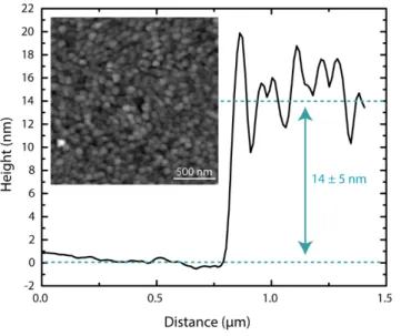
Figure 1: AFM height profile of the MA0.15FA0.85PbI3 thin film. The inset shows the AFM image of the perovskite film, with a grain
size distribution of 50 ± 20 nm.
perovskite film. Figure 1 shows a line profile across a boundary of the perovskite film and the underlying substrate yielding a perovskite film thickness of ~14 nm. The inset shows the morphology of the perovskite film, highlighting the small grain size of ~50 nm (compare also SI Figure S1 & S2). This grain size has previously been shown to be large enough to have a true “bulk” behavior of the excited charge carriers and avoid any quantum confinement effects which may change the underlying carrier dynamics.37 Quantum confinement effects are known to
increase the bandgap of semiconductors. We further confirm the lack of energetic confinement and thus, the bulk-like behavior of our MA0.15FA0.85PbI3 thin films by steady-state
photoluminescence (PL) spectroscopy (Figure 2a, brown), where we see the peak emission at the expected value of ~1.55 eV (800 nm) for bulk MA0.15FA0.85PbI3.38
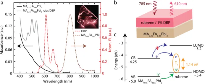
The absorbance of the neat MA0.15FA0.85PbI3 thin film (black line) and of the bilayer
upconversion device (gray), as well as the emission at 610 nm of the upconverted light (red) are shown in Figure 2a. The inset shows the upconverted light created in the upconversion device under 785 nm illumination, observed as the orange line running horizontally through the device. Figure 2b depicts the upconversion device structure investigated here consisting of the 15 nm thin film of MA0.15FA0.85PbI3, with a subsequent layer of rubrene/1% DBP spin coated from a 10
mg/ml stock solution.
In Figure 2c the band diagrams of the MA0.15FA0.85PbI3 perovskite and rubrene are shown.16,38
Two triplet sensitization mechanisms are possible: i) direct triplet exciton transfer (TET) of a bound triplet exciton as reported previously for quantum confined perovskite nanocrystals39 or as
in the case of PbS sensitized upconversion15,16 and ii) sequential electron and hole transfer
resulting in a bound triplet on the rubrene molecule.
interface, the combined rate of exciton diffusion to the interface and TET must outcompete the exciton dissociation rate. However, as discussed previously, lead halide perovskites exhibit binding energies below kT and the initially optically excited band-edge excitons generally rapidly dissociate within picoseconds. Hence, TET from these band-edge excitons is unlikely to be the dominant mechanism of triplet sensitization at room temperature by the bulk perovskite investigated here. However, shallow traps may result in localized “long-lived” sub-bandgap excitons which could to transfer to the rubrene layer within their lifetime.40
Figure 2: (a) Normalized absorbance spectra of a neat MA0.15FA0.85PbI3 perovskite film (black), MA0.15FA0.85PbI3/rubrene/1%DBP
bilayer device (gray), the upconverted emission stemming from rubrene/DBP (red) and the NIR emission of the MA0.15FA0.85PbI3
perovskite (brown). The inset shows the device under 785 nm illumination, and the upconverted light is seen as the orange line. (b) Schematic of the bilayer upconversion device, which emits 610 nm light upon 785 nm excitation. (c) Band diagram of MA0.15FA0.85PbI3 and rubrene, showing the energetically favored hole transport from the perovskite VB to the rubrene HOMO. The
electron cannot directly transfer from the perovskite CB to the rubrene LUMO due to an energy barrier of ~1eV.
The energetic alignment indicates that hole transfer from the perovskite valence band (VB) to the rubrene highest occupied molecular orbital (HOMO) can be very efficient due to the driving energy of ~0.4 eV. An unbound electron on the other hand, cannot transfer directly into the lowest unoccupied molecular orbital (LUMO) of rubrene due to the ~1 eV energy gap between the
perovskite conduction band (CB) and the rubrene LUMO, despite significant band bending reported by Ji et al.41 However, with a hole residing on the rubrene molecule, it may be possible
to transfer the electron directly into the bound triplet state (T1) through a mediating
charge-transfer state (CT) at the interface.
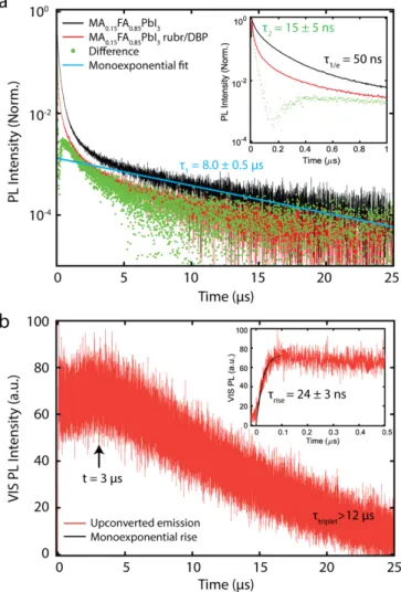
To further investigate the upconversion process, as well as determine the timescale of triplet sensitization, we turn to resolved transient PL spectroscopy. Figure 3a shows the time-resolved NIR PL of a neat MA0.15FA0.85PbI3 film (black trace), and of the bilayer upconversion
device (red trace). Both decay traces show highly multiexponential dynamics, indicating a broad distribution of emission rates. To avoid overfitting, we define the PL lifetime of the neat MA0.15FA0.85PbI3 as the time in which the population decays to 1/e (t1/e = 50 ns). The very long
tail (t1 = 8 µs) is attributed to delayed fluorescence stemming from trapped carriers.42
Interestingly, we observe that the overall emission intensity of the MA0.15FA0.85PbI3 perovskite
film is not notably quenched as previously seen in PbS NC-based devices,15,16 despite seeing a
decrease in the PL lifetime. This residual NIR PL intensity can likely be attributed to carriers that radiatively recombine in the “bulk” of the perovskite film prior to reaching the extraction point at the MA0.15FA0.85PbI3/rubrene interface. In addition, the organic molecules can passivate
dangling bonds at the surface of the perovskite lattice. This reduces non-radiative recombination occurring at surface defects in the MA0.15FA0.85PbI3 perovskite film, thus increasing the overall
PLQY.43,44
To extract the dynamics of energy transfer process at the MA0.15FA0.85PbI3/rubrene interface, we
apply our previously introduced extraction method,15,16 where we subtract the residual NIR PL
dynamics of the neat MA0.15FA0.85PbI3 film from the dynamics of the bilayer device. This method
to the rubrene and is quenched by the added upconverting layer, while the inactive population does not interact with the rubrene. This can be due to the morphology of the rubrene layer (e.g. pinholes in the rubrene film), or be a result of carriers which radiatively recombine within the thin perovskite film prior to reaching the inorganic/organic interface. The transfer kinetics obtained by this method are seen in Figure 3a as green dots. We find a characteristic decay time of t2 = 15 ± 5 ns (dark blue), highlighted in the inset in Figure 3a, which shows a magnification of the early time dynamics. The observed subsequent rise and slow decay in the extracted transfer dynamics (green dots) at later times can be attributed to back transfer of singlet excitons created after diffusion-mediated TTA.16
The extracted transfer time is slower than reported previously for quenching by hole- or electron-acceptors30,45 and may indicate the presence of a long-lived state which mediates the energy
transfer process as observed previously in triplet sensitization by PbS NCs46,47 or could stem from
an energy barrier for the electron transfer process due to the reported band bending at the perovskite/rubrene interface.41
To further investigate the upconversion mechanism, we investigate the dynamics of the upconverted emission, which correlate to a convolution of the rate of energy transfer, diffusion-mediated TTA in rubrene and the emission from DBP following FRET. Figure 3b highlights the transient PL spectroscopy performed on a bilayer device when monitoring the DBP emission. The inset shows an enlargement of the PL dynamics at a short time scale. We observe that the long-lived triplets (ttriplet > 12 µs) have not fully decayed at 25 µs, which results in a buildup of triplet excitons in the rubrene film that do not decay between pulses. An increase in the triplet population has been shown to increase the rate of TTA, which results in an apparent reduction in the extracted characteristic time for TTA, as well as the extracted triplet lifetime.15,16 The
extracted rise time trise = 24 ± 3 ns of the upconverted emission therefore portrays only a lower bound for the rate of the total upconversion process. Interestingly, the peak emission does not occur until t = 3 µs, and a second slower rise is observed leading up to this time. We attribute this to additional delayed TTA caused by slow triplet diffusion and by delayed triplet generation by thermally detrapped carriers, which can occur in addition to the prompt transfer of free carriers.
Figure 3: (a) Time-resolved PL dynamics of the NIR emission from neat MA0.15FA0.85PbI3 (black), the quenched NIR dynamics of
MA0.15FA0.85PbI3 in the bilayer device (red) under 785 nm excitation. The trapped carrier lifetime (t1 = 8 µs) is extracted from the
long-time dynamics (light blue). The extracted dynamics (green) yield an extracted quenching rate of t2 = 15 ± 5 ns. (b) Dynamics
of the upconverted light emitted from the bilayer device. The rise time gives an upper bound for the triplet sensitization rate (trise
However, as both bound triplet excitons and free carriers (holes) can be present in the rubrene layer, triplets may be annihilated not only by TTA, but also through triplet-charge annihilation (TCA). In the TCA process, a bound triplet exciton collides with an adjacent single charge and either scatters it, or the collision dissociates the bound triplet exciton into free charges. Therefore, this latter mechanism creates more freely diffusing charges in the film which can undergo TCA, effectively reducing the achievable upconverted PL.35,48 To further elucidate roles of TCA and
TTA we investigate the magnetic field effect (MFE) of the upconverted light, as well as the power dependence of the emission, both of which exhibit features unique to TTA.
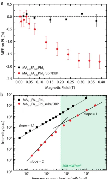
The theory of MFEs in molecular crystals was first developed by Merrifield in 1968.49,50 When
two triplet excitons collide, one of nine possible triplet-triplet pair states is formed. Only those with singlet character can effectively couple to the singlet state. The external magnetic field can modify the number of states with singlet character. At zero field only three of the nine states have singlet character, and as the field is increased, additional states acquire singlet character, thus increasing the rate of TTA. At high fields, the singlet character is localized on only two pair states, and therefore the yield of TTA is reduced, resulting in the negative MFE typical of TTA. Figure 4a shows the MFEUC of the upconverted emission from a
MA0.15FA0.85PbI3/rubrene/1%DBP bilayer device, which shows the typical signature of TTA (red
hexagons). The MFEPL of a neat MA0.15FA0.85PbI3 film under 532 nm excitation is shown as black
squares, and despite reports of negative MFEs (up to 2.5% on photocurrent at 300mT) in similar perovskite thin films35,51 we are not able to unambiguously detect an effect by the applied
magnetic field.
Furthermore, the power dependency of the MA0.15FA0.85PbI3 PL (~800 nm) and of the
pulsed excitation at 10 MHz is highlighted in the log-log plot in Figure 4b (compare also to SI Figure S3). The MA0.15FA0.85PbI3 PL (black squares) shows a slightly super-linear power
dependency, with a slope of 1.1 (gray line) indicating the emission primarily stems from monomolecular recombination in the perovskite thin film, consistent with previous reports of shallow-trap-assisted recombination.29,52,53
The upconverted emission (red hexagons) shows the transition of the slope from quadratic (slope = 2) to linear (slope = 1), which is typical of bimolecular TTA.54 In the weak annihilation regime
(lower powers) triplets decay primarily via quasi first-order kinetics and the upconverted PL intensity is quadratic with excitation power (white background). At higher powers (strong annihilation regime), the triplets decay primarily through bimolecular TTA, resulting in a linear dependence of the upconversion efficiency and the excitation power (green background). As a result, the upconversion efficiency is dependent on the excitation power and the maximal upconversion efficiency is obtained in the linear regime. In the MA0.15FA0.85PbI3/rubrene/1%DBP bilayer devices this quadratic-to-linear transition occurs at
500 mW/cm2 (dashed green line) average incident power under pulsed excitation, nearly an order
of magnitude lower than the incident power required in previous PbS NC-based upconversion devices,15 and two-fold less than in interference enhanced upconversion devices.15
Finally, we investigate the upconversion efficiency (𝜂"#) of the bilayer device. 𝜂"# is defined as the fraction of excited carriers in the sensitizer that are converted to singlet excitons in the annihilator,6 which is the product of the energy transfer efficiency from sensitizer to annihilator
(𝜂$%) and the TTA efficiency of the annihilator (𝜂%%&). On the other hand, the external quantum efficiency (EQE) is the ratio of number of upconverted visible photons to number of incident infrared photons. In our bilayer device, this is further equivalent to the product of absorption of
MA0.15FA0.85PbI3 at 785nm excitation (𝐴𝑏𝑠*+,-.), the upconversion efficiency (𝜂"#/2), and the
PLQY of rubrene:1 wt.% DBP film (𝜂12:456) at visible excitation, as shown in equation (1): 𝐸𝑄𝐸 = 𝐴𝑏𝑠*+,-.∙ (<=>
? ) ∙ 𝜂12:456 (1)
Note that 𝜂"# is divided by 2 to normalize to a maximum efficiency of 100%. Both the EQE of the bilayer device under 785nm excitation and 𝜂12:456 at 450nm excitation are measured with an integrating sphere,55 giving an EQE of (1.5 ± 0.3) ×10-4 % and 𝜂
12:456 of 9.3 ± 0.8 %.
However, due to the very low absorption of MA0.15FA0.85PbI3 thin films at the excitation
wavelength of 785 nm, and parasitic interference effects, it is difficult to accurately measure the percentage of absorbed photons (compare also SI Figure S4). We estimate the upper bound of the absorption to be 0.1%, which yields a conservative estimate for the internal upconversion efficiency of 𝜂"# = 3.1%.
In conclusion, we have been able to show that MA0.15FA0.85PbI3 thin films can function as
efficient triplet sensitizers of the annihilator rubrene. The presented results show that TTA is the prevalent process observed in the MA0.15FA0.85PbI3/rubrene/1%DBP bilayer device, with no
detectable detrimental effect caused by TCA. The extracted triplet sensitization rate of t = 15 ns is unusually slow for an electron transfer process and may point to a long-lived intermediate localized bound excitonic state mediating the energy transfer process, or an energy barrier for the electron transfer at the interface stemming from the reported band bending and will be subject to further investigation. Optimization of the energy transfer process, the energetic band alignment in the upconversion device, as well as the device structure provide a means to further improve the device performance.
Figure 4: (a) Change in the upconverted emission (red hexagons) and the NIR MA0.15FA0.85PbI3 emission (black squares) under
an applied magnetic field. (b) Power dependency of the NIR emission of the MA0.15FA0.85PbI3 perovskite in a bilayer device, showing
a slightly super-linear trend (black squares). The upconverted emission (red hexagons) shows the quadratic-to-linear slope change typical of TTA, with an average incident power density threshold of 500 mW/cm2.
ASSOCIATED CONTENT Supporting Information
The Supporting Information is available free of charge at DOI:
Experimental section, additional AFM data (Figure S1 & S2), upconverted PL dynamics during the power dependency (Figure S3), and the absorbance spectra of the bilayer device showing the
parasitic absorption effects (Figure S4).
AUTHOR INFORMATION Corresponding Author
*Lea Nienhaus: nienhaus@chem.fsu.edu *Moungi G. Bawendi: mgb@mit.edu *Marc A. Baldo: baldo@mit.edu
Present address
&Department of Chemistry and Biochemistry, Florida State University, Tallahassee, FL 32306
ORCID Lea Nienhaus: 0000-0003-1412-412X Juan-Pablo Correa-Baena: 0000-0002-3860-1149 Sarah Wieghold: 0000-0001-6169-3961 Marc A. Baldo: 0000-0003-2201-5257 Moungi G. Bawendi: 0000-0003-2220-4365 Notes
The authors declare no competing financial interests.
ACKNOWLEDGEMENT
This work was supported as part of the Center for Excitonics, an Energy Frontier Research Center funded by the US Department of Energy, Office of Science, Office of Basic Energy Sciences under Award Number DE-SC0001088 (MIT). J.P.C.B. is supported by a postdoctoral fellowship awarded by the U.S. Department of Energy, Office of Science, Office of Energy Efficiency and Renewable Energy. S.W. was supported by the National Science Foundation (NSF) under Grant NSF CA No. EEC-1041895. N.D.K. was supported by the National Science Foundation Graduate
Research Fellowship under Grant No. 1122374 and funded by the US Department of Energy, Office of Basic Energy Sciences, Division of Materials Sciences and Engineering under Award No. DE-FG02-07ER46454. This work was supported in part at the Center for Nanoscale Systems (CNS), a member of the National Nanotechnology Coordinated Infrastructure Network (NNCI), which is supported by the National Science Foundation under NSF Award No. 1541959. CNS is part of Harvard University.
REFERENCES
(1) Shockley, W.; Queisser, H. J. Detailed Balance Limit of Efficiency of P-n Junction Solar Cells. J. Appl. Phys. 1961, 32 (3), 510–519.
(2) Trupke, T.; Green, M. A.; Würfel, P. Improving Solar Cell Efficiencies by Up-Conversion of Sub-Band-Gap Light. J. Appl. Phys. 2002, 92 (7), 4117–4122.
(3) Meng, F.-L.; Wu, J.-J.; Zhao, E.-F.; Zheng, Y.-Z.; Huang, M.-L.; Dai, L.-M.; Tao, X.; Chen, J.-F. High-Efficiency near-Infrared Enabled Planar Perovskite Solar Cells by Embedding Upconversion Nanocrystals. Nanoscale 2017, 9 (46), 18535–18545.
(4) He, M.; Pang, X.; Liu, X.; Jiang, B.; He, Y.; Snaith, H.; Lin, Z. Monodisperse Dual-Functional Upconversion Nanoparticles Enabled Near-Infrared Organolead Halide Perovskite Solar Cells. Angew. Chem. 2016, 128 (13), 4352–4356.
(5) Wang, F.; Banerjee, D.; Liu, Y.; Chen, X.; Liu, X. Upconversion Nanoparticles in Biological Labeling, Imaging, and Therapy. Analyst 2010, 135 (8), 1839–1854.
(6) Zhou, J.; Liu, Q.; Feng, W.; Sun, Y.; Li, F. Upconversion Luminescent Materials: Advances and Applications. Chem. Rev. 2015, 115 (1), 395–465.
(7) Deng, R.; Qin, F.; Chen, R.; Huang, W.; Hong, M.; Liu, X. Temporal Full-Colour Tuning through Non-Steady-State Upconversion. Nat. Nanotechnol. 2015, 10 (3), 237.
(8) Schmidt, T. W.; Castellano, F. N. Photochemical Upconversion: The Primacy of Kinetics. J. Phys. Chem. Lett. 2014, 5 (22), 4062–4072.
(9) Schulze, T. F.; Schmidt, T. W. Photochemical Upconversion: Present Status and Prospects for Its Application to Solar Energy Conversion. Energy Environ. Sci. 2014, 8 (1), 103–125.
(10) Singh-Rachford, T. N.; Castellano, F. N. Photon Upconversion Based on Sensitized Triplet–Triplet Annihilation. Coord. Chem. Rev. 2010, 254 (21), 2560–2573.
(11) Mahboub, M.; Huang, Z.; Tang, M. L. Efficient Infrared-to-Visible Upconversion with Subsolar Irradiance. Nano Lett. 2016, 16 (11), 7169–7175.
(12) Dexter, D. L. A Theory of Sensitized Luminescence in Solids. J. Chem. Phys. 1953, 21, 836–850. (13) Monguzzi, A.; Tubino, R.; Meinardi, F. Multicomponent Polymeric Film for Red to Green Low
Power Sensitized Up-Conversion. J. Phys. Chem. A 2009, 113 (7), 1171–1174.
(14) Amemori, S.; Sasaki, Y.; Yanai, N.; Kimizuka, N. Near-Infrared-to-Visible Photon Upconversion Sensitized by a Metal Complex with Spin-Forbidden yet Strong S 0 –T 1 Absorption. J. Am. Chem.
Soc. 2016, 138 (28), 8702–8705.
(15) Wu, M.; Congreve, D. N.; Wilson, M. W. B.; Jean, J.; Geva, N.; Welborn, M.; Van Voorhis, T.; Bulović, V.; Bawendi, M. G.; Baldo, M. A. Solid-State Infrared-to-Visible Upconversion Sensitized by Colloidal Nanocrystals. Nat. Photonics 2016, 10 (1), 31–34.
(16) Nienhaus, L.; Wu, M.; Geva, N.; Shepherd, J. J.; Wilson, M. W. B.; Bulović, V.; Van Voorhis, T.; Baldo, M. A.; Bawendi, M. G. Speed Limit for Triplet-Exciton Transfer in Solid-State PbS Nanocrystal-Sensitized Photon Upconversion. ACS Nano 2017, 11 (8), 7848–7857.
(17) Nienhaus, L.; Wu, M.; Bulovic, V.; Baldo, M. A.; Bawendi, M. G. Using Lead Chalcogenide Nanocrystals as Spin Mixers: A Perspective on near-Infrared-to-Visible Upconversion. Dalton Trans 2018, 47, 8509–8516.
(18) Huang, Z.; Li, X.; Mahboub, M.; Hanson, K. M.; Nichols, V. M.; Le, H.; Tang, M. L.; Bardeen, C. J. Hybrid Molecule–Nanocrystal Photon Upconversion Across the Visible and Near-Infrared. Nano Lett. 2015, 15 (8), 5552–5557.
(19) Wu, M.; Jean, J.; Bulović, V.; Baldo, M. A. Interference-Enhanced Infrared-to-Visible
Upconversion in Solid-State Thin Films Sensitized by Colloidal Nanocrystals. Appl. Phys. Lett. 2017, 110 (21), 211101.
(20) Scholes, G. D. LONG-RANGE RESONANCE ENERGY TRANSFER IN MOLECULAR SYSTEMS. Ann. Rev. Phys. Chem. 2003, 54, 57–87.
(21) Kim, J.; Wong, C. Y.; Scholes, G. D. Exciton Fine Structure and Spin Relaxation in Semiconductor Colloidal Quantum Dots. Acc. Chem. Res. 2009, 42 (8), 1037–1046.
(22) Kojima, A.; Teshima, K.; Shirai, Y.; Miyasaka, T. Organometal Halide Perovskites as Visible-Light Sensitizers for Photovoltaic Cells. J. Am. Chem. Soc. 2009, 131 (17), 6050–6051.
(23) Green, M. A.; Hishikawa, Y.; Dunlop, E. D.; Levi, D. H.; Hohl-Ebinger, J.; Ho-Baillie, A. W. Y. Solar Cell Efficiency Tables (Version 51). Prog. Photovolt. Res. Appl. 2017, 26 (1), 3–12. (24) Pellet, N.; Gao, P.; Gregori, G.; Yang, T.-Y.; Nazeeruddin, M. K.; Maier, J.; Grätzel, M.
Mixed-Organic-Cation Perovskite Photovoltaics for Enhanced Solar-Light Harvesting. Angew. Chem. Int. Ed. 2014, 53 (12), 3151–3157.
(25) Stoumpos, C. C.; Malliakas, C. D.; Kanatzidis, M. G. Semiconducting Tin and Lead Iodide Perovskites with Organic Cations: Phase Transitions, High Mobilities, and Near-Infrared Photoluminescent Properties. Inorg. Chem. 2013, 52 (15), 9019–9038.
(26) Tress, W. Perovskite Solar Cells on the Way to Their Radiative Efficiency Limit – Insights Into a Success Story of High Open-Circuit Voltage and Low Recombination. Adv. Energy Mater. 2017, 7 (14), 1602358.
(27) Galkowski, K.; Mitioglu, A.; Miyata, A.; Plochocka, P.; Portugall, O.; Eperon, G. E.; Wang, J. T.-W.; Stergiopoulos, T.; Stranks, S. D.; Snaith, H. J.; et al. Determination of the Exciton Binding Energy and Effective Masses for Methylammonium and Formamidinium Lead Tri-Halide Perovskite Semiconductors. Energy Environ. Sci. 2016, 9 (3), 962–970.
(28) Yang, Y.; Yang, M.; Li, Z.; Crisp, R.; Zhu, K.; Beard, M. C. Comparison of Recombination Dynamics in CH 3 NH 3 PbBr 3 and CH 3 NH 3 PbI 3 Perovskite Films: Influence of Exciton Binding Energy. J. Phys. Chem. Lett. 2015, 6 (23), 4688–4692.
(29) Yamada, Y.; Nakamura, T.; Endo, M.; Wakamiya, A.; Kanemitsu, Y. Photocarrier Recombination Dynamics in Perovskite CH3NH3PbI3 for Solar Cell Applications J. Am. Chem. Soc. 2014, 136, 11610-11613.
(30) Stranks, S. D.; Eperon, G. E.; Grancini, G.; Menelaou, C.; Alcocer, M. J. P.; Leijtens, T.; Herz, L. M.; Petrozza, A.; Snaith, H. J. Electron-Hole Diffusion Lengths Exceeding 1 Micrometer in an Organometal Trihalide Perovskite Absorber. Science 2013, 342 (6156), 341–344.
(31) Xing, G.; Mathews, N.; Sun, S.; Lim, S. S.; Lam, Y. M.; Grätzel, M.; Mhaisalkar, S.; Sum, T. C. Long-Range Balanced Electron- and Hole-Transport Lengths in Organic-Inorganic CH3NH3PbI3.
Science 2013, 342 (6156), 344.
(32) Tress, W.; Marinova, N.; Inganäs, O.; Nazeeruddin, M. K.; Zakeeruddin, S. M.; Graetzel, M. Predicting the Open-Circuit Voltage of CH3NH3PbI3 Perovskite Solar Cells Using
Electroluminescence and Photovoltaic Quantum Efficiency Spectra: The Role of Radiative and Non-Radiative Recombination. Adv. Energy Mater. 2014, 5 (3), 1400812.
(33) Ponseca, C. S.; Savenije, T. J.; Abdellah, M.; Zheng, K.; Yartsev, A.; Pascher, T.; Harlang, T.; Chabera, P.; Pullerits, T.; Stepanov, A.; et al. Organometal Halide Perovskite Solar Cell Materials
Rationalized: Ultrafast Charge Generation, High and Microsecond-Long Balanced Mobilities, and Slow Recombination. J. Am. Chem. Soc. 2014, 136 (14), 5189–5192.
(34) Even, J.; Pedesseau, L.; Jancu, J.-M.; Katan, C. Importance of Spin–Orbit Coupling in Hybrid Organic/Inorganic Perovskites for Photovoltaic Applications. J. Phys. Chem. Lett. 2013, 4 (17), 2999–3005.
(35) Lu, K.; Zhao, C.; Luan, L.; Duan, J.; Xie, Y.; Shao, M.; Hu, B. Exploring the Role of Spin-Triplets and Trap States in Photovoltaic Processes of Perovskite Solar Cells. J. Mater. Chem. C 2018, 6 (18), 5055–5062.
(36) Kafle, T. R.; Kattel, B.; Lane, S. D.; Wang, T.; Zhao, H.; Chan, W.-L. Charge Transfer Exciton and Spin Flipping at Organic–Transition-Metal Dichalcogenide Interfaces. ACS Nano 2017, 11 (10), 10184–10192.
(37) Anaya, M.; Rubino, A.; Rojas, T. C.; Galisteo-López, J. F.; Calvo, M. E.; Míguez, H. Strong Quantum Confinement and Fast Photoemission Activation in CH3NH3PbI3 Perovskite Nanocrystals Grown within Periodically Mesostructured Films. Adv. Opt. Mater. 2017, 5 (8), 1601087.
(38) Correa-Baena, J. P.; Steier, L.; Tress, W.; Saliba, M.; Neutzner, S.; Matsui, T.; Giordano, F.; Jacobsson, T. J.; Srimath Kandada, A. R.; Zakeeruddin, S. M.; et al. Highly Efficient Planar Perovskite Solar Cells through Band Alignment Engineering. Energy Environ. Sci. 2015, 8 (10), 2928–2934.
(39) Mase, K.; Okumura, K.; Yanai, N.; Kimizuka, N. Triplet Sensitization by Perovskite Nanocrystals for Photon Upconversion. Chem. Commun. 2017, 53 (59), 8261–8264.
(40) He, H.; Yu, Q.; Li, H.; Li, J.; Si, J.; Jin, Y.; Wang, N.; Wang, J.; He, J.; Wang, X.; et al. Exciton Localization in Solution-Processed Organolead Trihalide Perovskites. Nat. Commun. 2016, 7, 10896.
(41) Ji, G.; Zheng, G.; Zhao, B.; Song, F.; Zhang, X.; Shen, K.; Yang, Y.; Xiong, Y.; Gao, X.; Cao, L.; et al. Interfacial Electronic Structures Revealed at the Rubrene/CH3NH3PbI3 Interface. Phys. Chem. Chem. Phys. 2017, 19 (9), 6546–6553.
(42) Chirvony, V. S.; González-Carrero, S.; Suárez, I.; Galian, R. E.; Sessolo, M.; Bolink, H. J.; Martínez-Pastor, J. P.; Pérez-Prieto, J. Delayed Luminescence in Lead Halide Perovskite Nanocrystals. J. Phys. Chem. C 2017, 121 (24), 13381–13390.
(43) Luo, D.; Yang, W.; Wang, Z.; Sadhanala, A.; Hu, Q.; Su, R.; Shivanna, R.; Trindade, G. F.; Watts, J. F.; Xu, Z.; et al. Enhanced Photovoltage for Inverted Planar Heterojunction Perovskite Solar Cells. Science 2018, 360 (6396), 1442.
(44) Yavari, M.; Mazloum-Ardakani, M.; Gholipour, S.; Tavakoli, M. M.; Taghavinia, N.; Hagfeldt, A.; Tress, W. Reducing Surface Recombination by a Poly(4-Vinylpyridine) Interlayer in
Perovskite Solar Cells with High Open-Circuit Voltage and Efficiency. ACS Omega 2018, 3 (5), 5038–5043.
(45) Westbrook, R. J. E.; Sanchez-Molina, D. I.; Manuel Marin-Beloqui, D. J.; Bronstein, D. H.; Haque, D. S. A. Effect of Interfacial Energetics on Charge Transfer from Lead Halide Perovskite to Organic Hole Conductors. J. Phys. Chem. C 2018, 122 (2), 1326–1332.
(46) Bender, J. A.; Raulerson, E. K.; Li, X.; Goldzak, T.; Xia, P.; Van Voorhis, T.; Tang, M. L.; Roberts, S. T. Surface States Mediate Triplet Energy Transfer in Nanocrystal–Acene Composite Systems. J. Am. Chem. Soc. 2018, 140 (24), 7543–7553.
(47) Garakyaraghi, S.; Mongin, C.; Granger, D. B.; Anthony, J. E.; Castellano, F. N. Delayed Molecular Triplet Generation from Energized Lead Sulfide Quantum Dots. J. Phys. Chem. Lett. 2017, 8 (7), 1458–1463.
(48) Shao, M.; Yan, L.; Li, M.; Ilia, I.; Hu, B. Triplet–Charge Annihilation versus Triplet–Triplet Annihilation in Organic Semiconductors. J. Mater. Chem. C 2013, 1 (7), 1330–1336.
(49) Merrifield, R. E. Theory of Magnetic Field Effects on the Mutual Annihilation of Triplet Excitons. J. Chem. Phys. 1968, 48 (9), 4318–4319.
(50) Merrifield, R. E.; Avakian, P.; Groff, R. P. Fission of Singlet Excitons into Pairs of Triplet Excitons in Tetracene Crystals. Chem. Phys. Lett. 1969, 3 (3), 155–157.
(51) Zhang, C.; Sun, D.; Sheng, C.-X.; Zhai, Y. X.; Mielczarek, K.; Zakhidov, A.; Vardeny, Z. V. Magnetic Field Effects in Hybrid Perovskite Devices. Nat. Phys. 2015, 11, 427.
(52) Shi, Z.-F.; Sun, X.-G.; Wu, D.; Xu, T.-T.; Tian, Y.-T.; Zhang, Y.-T.; Li, X.-J.; Du, G.-T. Near-Infrared Random Lasing Realized in a Perovskite CH3NH3PbI3 Thin Film. J. Mater. Chem. C 2016, 4 (36), 8373–8379.
(53) Blancon, J.-C.; Nie, W.; Neukirch, A. J.; Gupta, G.; Tretiak, S.; Cognet, L.; Mohite, A. D.;
Crochet, J. J. The Effects of Electronic Impurities and Electron–Hole Recombination Dynamics on Large-Grain Organic–Inorganic Perovskite Photovoltaic Efficiencies. Adv. Funct. Mater. 2016, 26 (24), 4283–4292.
(54) Cheng, Y. Y.; Khoury, T.; Clady, R. G. C. R.; Tayebjee, M. J. Y.; Ekins-Daukes, N. J.; Crossley, M. J.; Schmidt, T. W. On the Efficiency Limit of Triplet–Triplet Annihilation for Photochemical Upconversion. Phys. Chem. Chem. Phys. 2010, 12 (1), 66–71.
(55) Mello, J. C. de; Wittmann, H. F.; Friend, R. H. An Improved Experimental Determination of External Photoluminescence Quantum Efficiency. Adv. Mater. 1997, 9.