HAL Id: hal-01119380
https://hal.archives-ouvertes.fr/hal-01119380
Submitted on 21 May 2015HAL is a multi-disciplinary open access archive for the deposit and dissemination of sci-entific research documents, whether they are pub-lished or not. The documents may come from teaching and research institutions in France or abroad, or from public or private research centers.
L’archive ouverte pluridisciplinaire HAL, est destinée au dépôt et à la diffusion de documents scientifiques de niveau recherche, publiés ou non, émanant des établissements d’enseignement et de recherche français ou étrangers, des laboratoires publics ou privés.
Miniaturized and reconfigurable notch antenna based on
a BST ferroelectric thin film
Hung Viet Nguyen, Ratiba Benzerga, Caroline Borderon, Christophe
Delaveaud, Ala Sharaiha, Raphael Renoud, Claire Le Paven, Sabrina Pavy,
Kevin Nadaud, Hartmut Gundel
To cite this version:
Hung Viet Nguyen, Ratiba Benzerga, Caroline Borderon, Christophe Delaveaud, Ala Sharaiha, et al.. Miniaturized and reconfigurable notch antenna based on a BST ferroelectric thin film. Materials Research Bulletin, Elsevier, 2015, 67, pp.255-260. �10.1016/j.materresbull.2015.02.034�. �hal-01119380�
Miniaturized and reconfigurable notch antenna based on a BST
ferroelectric thin film
Hung Viet Nguyena,c , Ratiba Benzergaa,*, CarolineBorderonb, Christophe Delaveaudc, Ala
Sharaihaa, Raphael Renoudb, Claire Le Pavena, Sabrina Pavyb, Kevin Nadaudb, Hartmut W.
Gundelb
a Institut d’Electronique et de Télécommunications de Rennes (IETR), IUT Saint-Brieuc,
Université de Rennes 1, 22004 Saint-Brieuc, France
b IETR, Université de Nantes, 2 rue de la Houssinière, 44322 Nantes, France
c CEA-LETI, Minatec, 17 avenue des Martyrs, 38054 Grenoble Cedex 9, France
*Corresponding author. Tel. +332 96 60 96 61, [email protected]
Graphical abstract
Highlights
A miniature and agile antenna based on a BST MIM capacitor is simulated and made. Mn2+ doped BST thin films are synthesized by chemical deposition and spin coating.
Permittivity and losses of the BSTthinfilm are respectively 225 and 0.02 at 1GHz. A miniaturization rate of 70 % is obtained with a MIM capacitance of 3.7 pF.
A frequency tunability of 14.5% and a tunability performance of 0.04 are measured.
ABSTRACT
This work deals with the design, realization and characterization of a miniature and
frequency agile antenna based on a ferroelectric Ba0,80Sr0,20TiO3 thin film. The notch antenna
is loaded with a variable Metal/Insulator/Metal (MIM) capacitor and is achieved by a
monolithic method. The MIM capacitance is 3.7 pF, which results in a resonant frequency of
miniaturization rate is 70 %. The characterization of the antenna prototype shows a frequency
tunable rate of 14.5 % under an electric field of 375 kV/cm, with a tunability performance = 0.04.
Keywords: Oxides; Thin films; Chemical synthesis; Dielectric properties; Ferroelectricity
1. INTRODUCTION
The generalization of communicating systems in the objects of our private and
professional life contributes significantly to the development of miniature and agile antennas.
The use of a single reconfigurable antenna allows tuning its operating frequency to different
communications standards and so, permits replacing multiband antennas in standard devices.
This solution offers the possibility to dynamically change the resonance frequency of the
antenna through electrical means. The space consumption is greatly reduced for frequency
reconfigurable antennas as one single resonant element can be used to cover all the bands.
Furthermore, this element is designed for its highest targeted band of operation which results
in small size elements. In addition to smaller elements, size reduction in the radio frequency
(RF) chain can be achieved by passing some of the filter requirements on a narrow-band
antenna design. All these result in space-saving and thus miniaturization.
For the achievement of frequency agile antennas, many solutions have been proposed in
literature. The agility of the antenna comes from the modification of its electrical length; it
can be obtained, for example, by insertion of active components such as PIN diodes (Positive
Intrinsic Negative Diode) [1] or MEMS (Micro-Electro-Mechanical Systems) [2]. The agility
can be also obtained by using, as substrate of the antenna, materials with specific properties
controlled by an external stimulus (such as an electric or a magnetic field). For that solution,
ferrites) [5] have been studied. The use of ferroelectric materials, such as KTN (KTa1-x
NbxO3) [6], BST (Ba1-xSrxTiO3) [7], can be envisaged because of the agility of their
permittivity under DC electric bias.
In this work, we were interested in an original reconfigurable solution using ferroelectric
film, not as substrate of the antenna, but integrated in a localized agile component of the
antenna: a MIM (Metal/Insulator/Metal) variable capacitor (varactor) based on a BST
ferroelectric thin film. The chosen antenna is an open slot antenna (notch antenna) which
shows easy integration in printed circuit and significant miniaturization ratio when loaded
with a correctly positioned capacitor [8]. As the operating frequency of the antenna depends
on the value of the capacitor load, if this one is variable (by integrating the ferroelectric
layer), the antenna may be reconfigurable. The ferroelectric material involved in this study is
the perovskite Ba0,80Sr0,20TiO3 compound with a Curie temperature TC = 60°C [9]. For this
study, it is doped with 1.5%at. of manganese (Mn2+). The Manganese induces the decrease of
the oxygen vacancies in the ferroelectric thin film, which allows the reduction of the
dielectric losses [10]. Mn2+ doped Ba0,80Sr0,20TiO3 films (hereafter noted BST) are produced
by chemical solution route and spin-coating deposition [10,11]. Their growth is
polycrystalline on stainless steel or alumina substrate [10,12] and their permittivities () are in the range [200 - 500] depending on the Mn2+ doping level, with dielectric losses less than
0.02 at 1 MHz [10].
The present article is presented as follows: the topology of the studied antenna is first
presented along with simulations made by the Ansys HFSS software [13]. The manufacturing
of an antenna prototype is further exposed, followed by the characterization of the BST MIM
capacitor and the MIM loaded antenna.
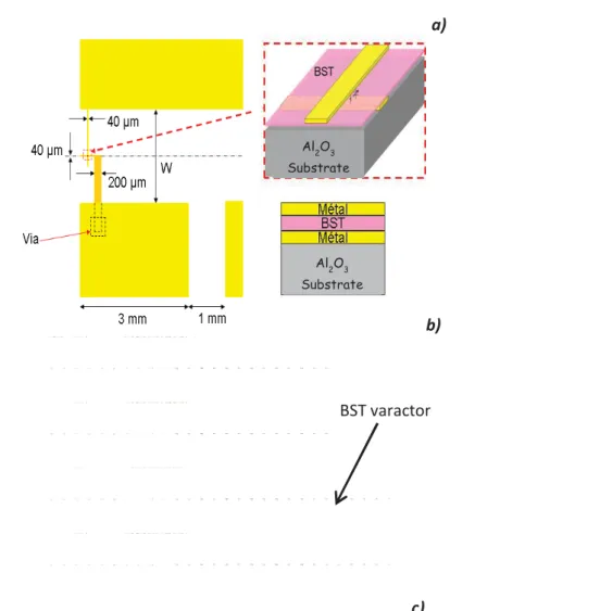
Figure 1.a shows the geometry of the studied antenna. The antenna is formed on an
alumina substrate of dimension of 25.4 x 25.4 mm² and thickness of 0.508 mm, coated by the
BST thin film and metallization layers.
The antenna structure consists of a notch cut from the edge of the ground plane; it is the
complementary structure of a conventional quarter wavelength monopole antenna. The notch
is etched at the top face of a printed circuit board (PCB) on the substrate. The notch is a
rectangular shape slot of width W = 2 mm and length L = 18 mm. For integration and design
purposes, the antenna is fed by 50 ohms microstrip line printed on the bottom face. A
capacitor, based on a BST thin film, is positioned at the end of the slot. The variation of the
permittivity of the BST thin film, by applying a DC bias voltage, allows the modification of
the electric length of the slot and so, induces a reconfigurabilty of the antenna. The detail of
the MIM topology is presented in Figure 1.b. For a better trade-off between antenna
efficiency and miniaturization rate, low values of capacitance (typically < 4 pF) have been chosen. For that purpose, the thickness of the BST film and the MIM capacitor area were
dimensioned at 1000 nm and 1600 m², respectively. The latter is obtained by the overlapping of the two orthogonal metallic electrodes of 40 microns-width. Two blocking
commercial capacitors are used to decouple the RF signal of the antenna to the applied
electric DC voltage; their capacitance is 56 pF.
This specific design was simulated under the Ansys HFSS software in order to validate the
chosen antenna topology. Simulations were performed with the following dimensions (Figure
1.a): W (slot width) = 2 mm; L (slot length) = 18 mm; Lf (length of the microstrip line) = 7
mm; a (power line position) = 8 mm.
To simulate the agility of the antenna, different values of the BST permittivity (from 250
to 150) were taken into account. These permittivities are those obtained under the applying of
Mn2+ [10]; corresponding dielectric losses were measured between 0.008 and 0.015 [10].
Here, to simplify simulation calculations, we assume constant losses equal to 0.02, greater
than the previously maximum measured value. The variation of corresponds to a permittivity agility A = 40 %. The agility A is defined using the following relation:
max min max
A
(Eq. 1)where max and min are the maximum and minimum values of the permittivity of the BST
film.
Figure 2 shows the simulated S11 reflection parameter of the antenna as a function of the
frequency. A shift of the resonant frequency from 640 MHz to 800 MHz is obtained when decreases and corresponds to an antenna frequency tunable rate TR of 22 %. TR is calculated
by:
( ) ( )
/2 ) ( ) ( max min max min
f f f f TR (Eq. 2)where f(min) and f(max) are the resonant frequencies of the antenna with, respectively,
minimum and maximum permittivity values of the BST film.
Given that the resonant frequency of the simulated antenna without BST MIM capacitor is
2.25 GHz, a miniaturization rate MR of 71 % is obtained on the size of the antenna. The
miniaturization rate is defined as:
Unloaded Unloaded Loaded f f f MR (Eq. 3)
where fLoaded is the resonant frequency of a MIM capacitor loaded antenna and fUnloaded is
3. IMPLEMENTATION OF THE NOTCH ANTENNA PROTOTYPE BASED ON A BST THIN
FILM
A monolithic implementation of the antenna prototype was performed. The variable MIM
structure capacitor based on the ferroelectric BST thin film was formed on the alumina
substrate by successive deposition of the lower electrode, the BST layer and the upper
electrode.
The lower electrode, made of 200 nm-thick layer of platinum, was first deposited. This
deposition was achieved through a mechanical mask by radio frequency (RF) magnetron
sputtering. The deposition of the Mn2+ doped Ba0,80Sr0,20TiO3 film was subsequently made by
chemical solution technique. The precursor solution was composed of barium and strontium
acetates to which a titanium n-propoxide and an organic stabilizer were mixed in appropriate
proportions. Details of the deposition parameters are summarized in [10,11]. The solution
was deposited on the substrate by spin-coating. A heat treatment at 750 °C allows the
evaporation of the organic material and the crystallization of the BST film in the ferroelectric
perovskite structure. Several steps "deposit by spin coating + heat treatment" were repeated to
obtain the required final BST film thickness. The BST thin film covers the entire surface of
the substrate.
Before the deposition of the upper electrode, the via connection to the lower electrode was
created by chemical etching of the BST layer [14]. The deposition of the top copper electrode
(1 micron thick), performed by RF-sputtering through a mechanical mask, completes the
geometry of the MIM varactor. The bottom electrode of this varactor is directly connected to
the upper edge of the slot, hence directly connected to the ground plane. The upper electrode
is connected to the small metallic patch P, and thus, the BST capacitor is formed. The RF
signal is coupled by 2 DC blocking capacitors of 56 pF. For DC voltage applying, one
small metallic patch P (Figure 1.a).
The loaded antenna prototype is shown in Figure 1.c. The ground plane of the antenna has
been expanded to facilitate its connection to the characterization device and also to improve
the antenna performance.
4. CHARACTERIZATION
4.1. BST CAPACITOR
The characterization in low frequencies of the MIM capacitor based on the BST film was
realized on an Agilent 4294A impedance-meter before the addition of the DC blocking
capacitors. It gives a capacitance value of 3.8 pF and dielectric losses tan = 0.02 at 1 MHz. Figure 3 shows the change of the capacitance as a function of the applied DC bias voltage. A
variation of the capacitance from 3.8 pF to 2.1 pF is observed when the DC voltage increases
from 0 V to 40 V (at 1 MHz); this corresponds to a permittivity agility A = 45 % (Eq. 1). The
rapid decline of the permittivity beyond 1 MHz and the discontinuity of the curves (after 8
MHz) are artificial and are due to the frequency limitation of the measurement technique.
Capacitance values in high frequencies are thus obtained by extrapolating the curves plotted
in low frequencies, as can be seen in Figure 3. At 1 GHz, the capacitance is estimated at 3.7
pF. Considering the actual dimensions of the MIM structure (surface of 1500 m2 and a BST
film thickness of 800 nm), a permittivity value of 225 is calculated for the deposited thin
film. At 1 GHz, the permittivity agility has been estimated at 40 % for a DC bias voltage of
40 V and at 35 % for a DC bias voltage of 30 V. These values are very close to those used in
simulations.
4.2. ANTENNA PROTOTYPE CHARACTERIZATION
presented in Figure 4. The measurement was performed using a vector network analyzer
(VNA Rohde Schwarz, working frequency range 0-24 GHz). The DC bias voltage was
controlled by a DC generator (QL 355 TTI, max voltage of 35 V). Figure 4 shows that the
resonant frequency of the antenna prototype shifts from 670 MHz to 774 MHz under the
application of a DC voltage varying from 0 to 30 V. This corresponds to a frequency tunable
rate TR of 14.5 % (Eq. 2). Considering the resonant frequencies of the BST loaded antenna
prototype (670 MHz) and the unloaded simulated antenna (2.25 GHz), the experimental
miniaturization rate is MR = 70 % (Eq. 3).
A retro-simulation of the antenna prototype response was performed by Ansys HFSS
software considering the real dimensions of the prototype and taking into account the
presence of the measuring cable. The matching of the retro-simulated resonant frequency to
the experimental one (Figure 5) was achieved by permittivity values of 220 (at 0 V) and 160
(at 30 V). These retro-simulated values are in agreement with the value of 225 obtained at 0
V and 1 GHz by extrapolation of measurements.
3D gain patterns of the antenna prototype were obtained by measuring the antenna in an
anechoic chamber (see supplementary data). As shown before in Figure 4, when the applied
voltage increased from 0 V to 30 V, the resonant frequency shifted from 670 MHz to 774
MHz. Ideally, the gain antenna measurements should cover both of these two frequencies;
however, the frequency limit of the instruments used during this characterization had
imposed measurements above 700 MHz. Gain patterns allow the calculation of the radiation
efficiency of the prototype for DC bias voltage of 0 and 30 V, as observed in Figure 6. Figure
6.a shows that the maximum radiation efficiency of the antenna is weak. This low level is
mainly explained by the miniaturization of the antenna, with very small electrical dimensions
(λ0/28 for the slot and λ0/11 x λ0/7 x λ0/900 for the ground plane at 700 MHz). Moreover, a
higher experimental losses than those simulated, introduced by the different materials
constituting the antenna prototype.
In Figure 6.b, one can observe that the radiation efficiency of the antenna increases with
the applied DC bias voltage. This can be explained by the fact that the permittivity of the
ferroelectric film decreases as the voltage increases, so that the operating point of the antenna
moves towards higher frequencies when loaded and the antenna appears electrically larger.
Consequently, an increase in gain is obtained, which induces an increase in radiation
efficiency. This is coherent with the fundamental laws of miniature antennas [15].
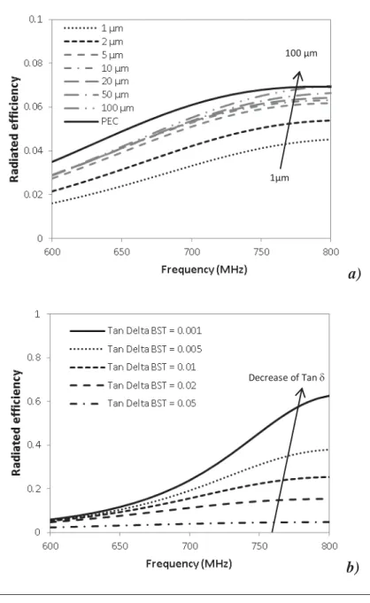
A study of the potential sources of losses responsible for the low antenna efficiency has
been carried out by simulation. Two effects have been studied: first, the thickness of the
copper metallization and thereafter, the BST dielectric loss. For the first study, the copper
metallization has been increased from 1 micron to 200 microns (Figure 7.a), maintaining
fixed dielectric properties of the BST layer (tan = 0.02 and = 160, obtained by retro-simulation of the BST loaded antenna measurement under DC voltage of 30 V). For the
second study, the BST thin film was simulated with dielectric loss tanδ decreasing from 0.05
to 0.001 (Figure 7.b), keeping the BST thickness equal to 1 μm.
First graph shows that the radiation antenna efficiency is improved when the thickness of
the metallization is increased, which is explained by the corresponding reduction of losses
introduced by the skin effect. Above 5 microns of metallization (which corresponds to 2
times the skin thickness at the frequency of 670 MHz) [16], the efficiency converges towards
that of a Perfect Electric Conductor (PEC), which theoretically does not possess losses.
Figure 7.b shows that the radiation efficiency of the antenna is strongly increased when the
dielectric losses of the BST material are decreased. With BST losses of 0.001, the efficiency
is more than 20 % for frequencies higher than 670 MHz. The efficiency is far higher (60 %)
to be taken into account in the design of miniaturized antennas.
To quantify the efficiency of the antenna frequency agility, a tunability performance () is defined as: min max E E TR
(Eq. 4)where Emax and Emin (kV/cm)are the electric bias fields used for the tuning control of the
BST thin film and TR is the antenna frequency tunable rate (here, the maximum voltage is 30
V, which corresponds to a maximum electric field of 375 kV/cm).
The calculated is 0.04. This is the best performance reported up to now in the literature (for example, = 0.03 in [17]) for a technology incorporating ferroelectric thin films in planar antennas. As mentioned before, higher performances could be obtained by increasing
the metallization thickness but also by improving the BST thin film dielectric losses.
5. CONCLUSION
In this work, a slot antenna, loaded with a tunable ferroelectric charge capacitor based on a
Mn2+ doped Ba0,80Sr0,20TiO3 thin film, was studied. The manufacturing of a prototype was
performed by monolithic method and validates the antenna design. The agility of the
permittivity of the BST ferroelectric thin film was extrapolated at about 35 % at 1 GHz for a
maximum electric field of 375 kV/cm. This induces an antenna frequency tunable rate of 14.5
%, corresponding to a tunabilty performance of 0.04. The loaded antenna prototype,
compared to the simulated antenna without the MIM structure and ferroelectric thin film, has
a degree of miniaturization of 70 %.
The authors want to thank CEA Leti and CNRS for their financial supports and
Cooksonelectronics Cholet for achieving the mechanical masks used during the electrodes
deposition.
REFERENCES
[1] J. -M. Laheurte, Switchable CPW-fed slot antenna for multifrequency operation,
Electron. Lett. 37 (2001) 1498 –1500.
[2] Z. Liu, K. Boyle, Joonas Krogerus, M. de Jongh, K. Reimann, R. Kaunisto, and J.
Ollikainen, MEMS-Switched, Frequency-Tunable Hybrid Slot/PIFA Antenna, IEEE
Antennas Wireless Propag. Lett. 8 (2009) 311–314.
[3] M. A. Abdalla and Z. Hu, Compact and tunable metamaterial antenna for multi-band
wireless communication applications, IEEE International Symposium on Antennas and
Propagation (2011) 1054 –1057.
[4] S. Missaoui, M. Kaddour, and A. Gharbi, Design and simulation reconfigurable liquid
crystal patch antennas on foam substrate, J. Chem. Eng. Mater. Sci. 2 (2011) 96–102.
[5] R. K. Mishra, S. S. Pattnaik, and N. Das, Tuning of microstrip antenna on ferrite
substrate, IEEE Trans. Antennas Propag. 41 (1993) 230 –233.
[6] Q. Simon, Y. Corredores, X. Castel, R. Benzerga, R. Sauleau, k. Mahdjoubi, A. Le
Febvrier, S. Deputier, M. Guilloux-viry, L. Zhang, P. Laurent, G. Tanne, Highly tunable
microwave stub resonator on ferroelectric KTa0.5Nb0.5O3 thin film, Appl. Phys. Lett. 99
(2011) 092904-1/3.
materials, Mater. Res. Innov. 2 (1999) 278-282.
[8] C. Lach, L. Rudant, C. Delaveaud, A. Azoulay, A new miniaturized antenna for ISM 433
MHz frequency band, Proceeding of European Conference on Antennas and Propagation
(EuCAP), Barcelona, Spain (2010) 1-5.
[9] B. A. Baumert, L. H. Chang, A. T. Matsuda T. L. Tsai, C. J. Tracy, R. B. Gregory, P. L.
Fejes, N. G. Cave, W. Chen, D. J. Taylor, T. Otsuki, E. Fujii, and S. Hayashi, K. Suu,
Characterization of sputtered barium strontium titanate and strontium titanate-thin films, J.
Appl. Phys. 82 (1997) 2558-2566.
[10] K. Nadaud, C. Borderon, S. Pavy, H.W. Gundel, Realization and characterization of
manganese doped BST thin films for reflectarray applications, Proceeding of IEEE
International Symposium on the Applications of Ferroelectric and Workshop on the
Piezoresponse Force Microscopy (ISAF/PFM), (2013) 145-148.
[11] C. Borderon, D. Averty, R. Seveno, and H. W. Gundel, Preparation and Characterization
of Barium Strontium Titanate Thin Films by Chemical Solution Deposition, Ferroelectrics
362 (2008) 1–7.
[12] C. Borderon, D. Averty, R. Seveno, H. W. Gundel, Influence of the Morphology of
Barium Strontium Titanate Thin Films on the Ferroelectric and Dielectric Properties, Integr.
Ferroelectr. 93 (2007) 133–140.
[13] Ansys, Ansys HFSS. 2012.
[14] S. Pavy, S. Baron, C. Borderon, and H. W. Gundel, Wet chemical etching of BaSrTiO3
ferroelectric thin films, Proc. International Symposium on Intergated Fonctionalities,
[15] L. J. Chu, Physical Limitations of Omni-Directional Antennas, J. Appl. Phys. 19 (1948)
1163–1175.
[16] E.C. Jordan, K. G. Balmain, Electromagnetic Waves and Radiating Systems, 2nd edition
1968, Prentice Hall, Chapter 5 (1968).
[17] H. Jiang, M. Patterson, D. Brown, C. Zhang, K. Pan, G. Subramanyam, D. Kuhl, K.
Leedy, and C. Cerny, Miniaturized and Reconfigurable CPW Square-Ring Slot Antenna
Loaded With Ferroelectric BST Thin Film Varactors, IEEE Trans. Antennas Propag. 60,
List of figure captions
Figure 1: a) Scheme of the notch antenna b) details of the varactor based on a BST thin film and c)
Photo of the notch antenna prototype loaded with a MIM varactor based on a BST thin film
Figure 2: Variation of the reflection parameter (S11) of the notch antenna according to the
permittivity of the BST thin film compared to an antenna without a BST MIM capacitor
Figure3: Evolution of the MIM capacitance based on the BST film as a function of the DC
voltage (with the extrapolation at 1 GHz)
Figure 4: Reflection parameter (S11) of the notch antenna prototype loaded by a BST
varactor
Figure 5: Measurement vs retro simulation of the reflection parameter (S11) of a notch
antenna loaded by a BST varactor
Figure 6: Measurement vs retro-simulation of the radiation efficiency of a notch antenna loaded by a
BST varactor under DC voltage of a) 0V and b) 30V
Figure 7: Simulated radiated efficiency of a notch antenna loaded by a BST varactor as a function of
Figure 1 a) b) c) Al2O3 Substrate Al2O3 Substrate BST varactor
Figure 3
V
Bias 0V40 V
Figure 6
a)
Figure 7 a) b) Decrease of Tan 1μm 100 μm