HAL Id: hal-00650046
https://hal.archives-ouvertes.fr/hal-00650046
Preprint submitted on 9 Dec 2011
HAL is a multi-disciplinary open access
archive for the deposit and dissemination of
sci-entific research documents, whether they are
pub-lished or not. The documents may come from
teaching and research institutions in France or
abroad, or from public or private research centers.
L’archive ouverte pluridisciplinaire HAL, est
destinée au dépôt et à la diffusion de documents
scientifiques de niveau recherche, publiés ou non,
émanant des établissements d’enseignement et de
recherche français ou étrangers, des laboratoires
publics ou privés.
Strained HgTe: a textbook 3D topological insulator
Clément Bouvier, Tristan Meunier, Philippe Ballet, Xavier Baudry, Roman
Kramer, Laurent Lévy
To cite this version:
Clément Bouvier, Tristan Meunier, Philippe Ballet, Xavier Baudry, Roman Kramer, et al.. Strained
HgTe: a textbook 3D topological insulator. 2011. �hal-00650046�
Strained HgTe: a textbook 3D topological insulator
Cl´ement Bouvier, Tristan Meunier, Roman Kramer, and Laurent P. L´evy
Institut N´eel, C.N.R.S.- Universit´e Joseph Fourier, BP 166, 38042 Grenoble Cedex 9, France
Xavier Baudry and Philippe Ballet
CEA, LETI, MINATEC Campus, DOPT, 17 rue des martyrs 38054 Grenoble Cedex 9, France (Dated: December 9, 2011)
Topological insulators can be seen as band-insulators with a conducting surface. The surface carriers are Dirac particles with an energy which increases linearly with momentum. This confers extraordinary transport properties characteristic of Dirac matter, a class of materials which elec-tronic properties are “graphene-like”. We show how HgTe, a material known to exhibit 2D spin-Hall effect in thin quantum wells,[1] can be turned into a textbook example of Dirac matter by opening a strain-gap by exploiting the lattice mismatch on CdTe-based substrates. The evidence for Dirac matter found in transport shows up as a divergent Hall angle at low field when the chemical potential coincides with the Dirac point and from the sign of the quantum correction to the conductivity. The material can be engineered at will and is clean (good mobility) and there is little bulk contributions to the conductivity inside the band-gap.
PACS numbers: 85.25.Cp, 03.65.Vf, 74.50.+r, 74.78.Na
Graphene research[2, 3] has stimulated a consider-able interest on Dirac matter, a novel class of materi-als where one or more bands have a Dirac-like disper-sion in the vicinity of the Fermi level. Newly discovered materials show that Dirac matter can take a variety of forms. For example, angle-resolved photo-emission ex-periments have measured bands with a linear spectrum below the Fermi level in topological insulators surface states[4], in organic conductors[5] and of course graphene stacks[6] with an odd number of layers. Transport ex-periments give smoking-gun evidences for Dirac fermions in graphene. For organic-conductors and topological-insulators, other contributions make transport data more difficult to unravel. This letter presents textbook evi-dences of Dirac fermions in a strained Mercury Telluride stack, using the low field magneto-transport behavior of a gated device.
Mercury (HgTe) and Cadmium (CdTe) Telluride have the same zinc-blende structure.[7] However compared to CdTe, HgTe has a band inversion at the Γ point: the Γ8 bands which have a P character lie 0.3 eV above
the Γ6 band (S character). When growing epitaxially
HgTe on top of CdTe, the HgTe lattice constant ex-pands to match the CdTe lattice, which applies a lat-eral strain to HgTe. As long as the HgTe thickness does not exceed a critical value above which dislocations ap-pear, the strain is homogenous through the material.[7] A number of papers[10] have pointed out that such strain opens a gap between the Γ8 light and heavy
hole bands, turning HgTe into a topological insulator.[8] The value of this gap can be engineered to some ex-tend in the epitaxial growth. In this work, a sym-metric Hg0.3Cd0.7Te/HgTe/Hg0.3Cd0.7Te stack (shown
in the inset of Fig. 1) was epitaxially grown on a CdTe [211] face. The direct gap between light and heavy
holes bands is estimated to be of order 11 meV while the indirect gap has been measured by thermal activa-tion transport to be ≈6 meV [supplementary material-a]. The Γ8 and Γ6 bands have a linear crossing[7] at
the HgTe/Hg0.3Cd0.7Te interface (different symmetries)
leading to 2D-“relativistic-like” surface bands which band velocity c plays the role of the speed of light. These surface states are one of the manifestations of the non-trivial topology of HgTe[10]. The dispersion of surface state in a strained material have been an-alyzed qualitatively from the surface local density of states[11] and in recent transport and magneto-optical experiments[12, 13]. Nevertheless quantitative data is not yet available for our stack structure: it is however relatively simple to infer the surface band and the Dirac point positions by scanning the gate within the gap in transport measurements.
A 200 µm long by 50 µm wide six-probes gated device has been made by etching the stack and contacting the top surface. The accessible range of gate voltages allows scanning part of the heavy-hole band (below Vg0≈ 0.8 V)
and the gap region (Vgbetween 1 and 6 V). An overview
of the sample resistivity is shown in Fig.1. The resistiv-ity is lowest (→ 1.2 kΩ at 6 V) in the gap area where the surface conduction dominates the transport. In the “hole region” (below 1 V), there is a co-existence between surface and bulk hole conduction. The mobility of heavy holes is low (large mass and short mean free path) lead-ing to a higher resistivity (≈ 4 kΩ) below 1 V in spite of the higher carrier density.
The hole and electron character of the conduction can be read-off directly from the Hall conductivity plot shown in Fig.3-top panel, where the slope at B=0 is negative at negative gate voltages and positive above Vg0. Note
2 -2 -1 0 1 2 3 4 5 6
V
g 1 2 3 4 5ρ
xx(k
Ω
)
T =1.5 K HgTe HgTe CdTe Hg Cd Te.7 .3 CdTe 30nm 30nm 100nm a-CdTe gate Hg Cd Te.7 .3 gate insulator 200nmFIG. 1: Inset: the 100nm thick HgTe slab is sandwiched be-tween two 30nm thick Hg0.3Cd0.7Te barriers. A 200 nm thick
amorphous CdTe layer on top serves as a gate insulator. Gate-voltage dependence of the resistivity. Vg0 ≈ 1V separates the electron and hole transport regimes: Above Vg0
trans-port is dominated by the surfaces while a coexistence with low-mobility heavy holes increases the resistivity below Vg0
from below or from above. These observations suggest an analysis of the magneto-transport using a two-fluid model: a surface contribution with a Dirac-like character and a bulk contribution.
The Lorentz force affects the motion of a relativistic charged particle with energy ǫ(~k) = ~c|~k| and momen-tum ~~k in a similar fashion as for a massive charged car-rier: the semiclassical equation of motion d~k
dt = − ec
~k × ~ˆ B
describes a cyclotron motion with angular frequency Ωc= eBc
2
ǫ(~k) which diverges at the Dirac point ǫ(k) → 0. In
the presence of the electric field E ˆx induced by the bias voltage and of particle collisions (specified by the scat-tering time τ ), the average particle velocity h~vi = chˆki drifts at an angle ΘHallwith respect to the electric field
tan ΘHall= σxy σxx = hvyi hvxi = Ωcτ = 2eD µ B = B B∗ , (1) where the particle energy has been replaced by the chemi-cal potential µ, D = c2τ /2 is the Dirac particles diffusion
coefficient, and the characteristic field B∗ = µ/(2eD) is proportional to the chemical potential. This Hall angle diverges at the Dirac point (µ → 0), a fundamental dif-ference with ordinary particles where ωcτ = eτmB does
not depend on energy.
The measured Hall angle slope (σxy/(σxxB)) is plotted
on Fig. 2-bottom: a cut-off divergence is observed close to the gate voltage Vg0 with an asymmetry between the
electron (Vg > Vg0) and the hole side. This
asymme-try comes from a partial population of bulk low-mobility heavy holes below Vg0 which also diffuse the Dirac
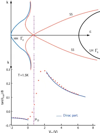
par--2 0 2 4 6 V (V)g -0.1 0.0 0.1 0.2 0.3 ta n (θH al l )/ B T =1.5K µD Dirac part. LH Γ8 HH Γ8 SS SS k k ε 8
FIG. 2: Bottom: plot of the Hall angle slope as a function of the gate voltage. An asymmetric cutt-off divergence is observed on each side of Vg0 consistent the expected
mag-netoconductance of Dirac particles. Vg0is interpreted as the
location of the Dirac point (µD) in gate voltage. The observed
asymmetry is attributed to a difference in diffusion coefficients on the electron (Vg > Vg0) and the hole side where the bulk
heavy hole band starts to be populated. Top: putting to-gether the analysis of the magneto-transport and activation data, the inferred positions of the heavy (HH) and light (LH) hole bands with respect to the surface states (SS) connecting them. The position of the Dirac point (Vg0= 0.8V) can also
be verified by extrapolating the observed n = 0 quantum Hall state to zero magnetic field[14].)
ticles because of their low mobilities. By contrast, the electron side of the Dirac dispersion lies inside the strain-induced Γ8 light-heavy holes gap. The observation of
this divergent Hall angle, very similar to graphene[15], is a strong evidence for Dirac particles at the HgTe sur-faces. A bulk hole conductivity σ0(Vg) appears below
Vg0, which is nearly field independent at low (¡1 T) field
(ωcτHH ≪ 1). Hence, the experimental
magnetoconduc-tance is dominated by the surface Dirac particles, which reads [supplementary-material-b] σD xx= kFℓe B2 ∗ B2+ B2 ∗ , σD xy= kFℓe BB∗ B2+ B2 ∗ , (2)
when expressed in units of the quantum of conductance, e2/h (ℓ
e= cτ is the mean free path, and kF = µ/(~c)).
ex-perimentally plotted in Fig. 3 are derived by inverting the measured resistivity tensor (ρxx, ρxy) and expressing
the data in units of e2/h [see a flash animation in the
supplementary-material-c]. Fits to the two fluid model σD
xx+ σ0 and σxyD, shown as dotted lines, are found to be
quite accurate for all gate voltages. The residual differ-ences between the data and fits is attributed below to the quantum corrections to the conductivity (antilocalization shown in Fig. 4).
A qualitative discussion of the data sheds some light on the origins of the parallel conduction σ0. At Vg≈ 1.75V
(≈ 1V above Vg0), the maximum of the Hall
magneto-conductance occurs at B=0.6 T. In Eq. 2 this maximum is at B∗= 2eD/µ(Vg) where the Hall conductance equals
kFℓe/2. Since B∗and kFℓefully specify the Dirac
magne-toconductance, the value of σ0, the parallel conductance,
is found to be of order one in units of e2/h. The value of σ0 varies little above Vg0 but increases linearly in the
hole region up-to ≈ 4.5e2/h@ Vg= −2 V. In this region,
σ0 measures the gradual population of the bulk heavy
-1.0 -0.5 0.0 0.5 1.0 B (T ) 5 10 15 20 σx x (e / h ) 2 -2 -0.25 1.75 5 V (V)g -5 0 5 σ x y -0.25 -2 1.75 5 V (V)g (e / h ) 2
FIG. 3: Longitudinal σxxand Hall σxy magnetoconductance
expressed in units of e2
/h. The solid lines are obtained by in-verting the measured resistivity tensor (ρxx, ρxy) and
rescal-ing in units of e2
/h. The dashed lines are obtained by fitting the experimental curves to σD
xx+ σ0 and σxyD. The difference
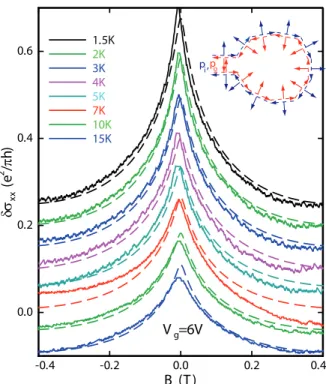
between the experimental curves and the fit are analyzed in terms of the quantum correction to the conductivity (weak-antilocalization) in Figure 4. -0.4 -0.2 0.0 0.2 0.4 B (T ) 0.0 0.2 0.4 0.6 δσ x x (e 2 /π h ) 1.5K 2K 3K 4K 5K 7K 10K 15K Vg=6V pi,po
FIG. 4: The quantum correction to the conductivity are ob-tained by subtracting the two-fluid fit to the measured longi-tudinal conductivity. The difference are plotted as a function of magnetic field for different temperatures. The curves are fitted to the expected digamma dependence as a function of field. The characteristic field is Bi= 40 mT at T=1.5 K and
increases with increasing temperature. Beyond Bi, the fitted
curves (dotted lines) are dominated by the logarithmic tails expected in 2D.
hole subbands. The non-zero Vg-independent value of
σ0 found in the gap region is more surprising. In this
experiment, the transport is measured by contacting the top faceof the HgTe slab. The sample has identical bar-riers on the top and bottom faces: the latter conduction is also expected to be dominated by 2D-Dirac carriers. Based on high field data,[14] we know that two faces are indeed connected through a ˜25 kΩ series-resistance[20], which explains the apparent gap conduction σ0.
Strained HgTe appears to be an almost ideal topolog-ical insulator for transport studies: • the MBE growth yields easily gated devices with clean interface where mo-bilities (≈ 3 104cm2/sec.) are already comparable to
graphene; • the Dirac point lies in the gap, and the gap conduction is dominated by the surface Dirac carriers; • the bulk conduction is always very low, and in the coex-istence region with the heavy hole band there is a natural mobility-selection of the surface carriers.
A resistance can be expressed as a probability of re-turn to the origin of charge carriers. In two dimen-sions, this probability strongly depends on closed-loops paths. There are two “time-reversed” directions along which charge particles can travel along each closed loop. For loop sizes smaller than the phase coherence length,
4 the propagation amplitudes add coherently. Depending
on their relative phase, this can increase or decrease the probability of return to the origin. For topological insu-lator surface states, the spin stays perpendicular to the momentum after a scattering event (spin-orbit interac-tions, see Fig. 4-inset). After the sequence of scatter-ing on a closed loop, the spin has undergone a 2π rota-tion, which affects the accumulated phase (sign change): For a given loop, the return probability is proportional to |ui(~p, ↑) + Θui(−~p, ↓)|2, where Θ represents the
time-reverse operation: since Θui(−~p, ↓) = −e2πΦ/Φ0ui(~p, ↑),
the return probability is proportional to sin22πΦ Φ0. The sign change comes from the spin rotation and the phase factor e2πΦ/Φ0 is the accumulated Aharonov-Bohm phase along the loop (Φ is the flux through the loop and Φ0 = h/e the flux quantum). The return probability
is minimal at zero magnetic field, i.e. the quantum cor-rection to the conductivity of the Dirac surface states are negative: this sign is opposite compared to ordinary con-ductors. Such “anti-localization” quantum corrections to the conductivity have been observed in graphene[18] and other Dirac matter compounds[19] and reveal the pres-ence of a Dirac point[16]. These quantum corrections to the conductivity are obtained by subtracting the two-fluid fit to the measured longitudinal conductivity and plotted in Fig. 4. Their magnetic field dependence can be fitted to the known dependence[16, 17] [supplementary information-d]. At 1.5 K, the magnitude of the weak-localization correction are ≈ 0.5 times smaller than the expected magnitude e2/(2πh) for a perfect Dirac cone.
The characteristic field Bi = Bso + Bφ(T ) has a
tem-perature independent contribution Bso ≈ 40 mT, which
we attribute to an interfacial spin-orbit scattering length ℓso ≈ 250 nm. For fields B > Bi, the expected long
loga-rithmic tails dominate the field dependence. In the hole region, the magnitude of quantum corrections drop by a factor of 2.5 and Bi increase by the same factor as ℓso is
reduced by the diffusion with heavy holes.
Strained HgTe appears to be a textbook realization of a 3D topological insulator. Evidence for the Dirac point come from • the observed divergence of the Hall angle at the gate voltage Vg0, • the sign and field dependence
of the quantum correction to the conductivity. Within the strain-induced gap, the conduction is dominated by the 2D Dirac carriers. In the coexistence region with the bulk heavy holes, the surface state conduction is re-duced by the diffusion between surface and bulk carriers. The processing and gating of this system is easy, making the fabrication of more complex structures (hybrids and spintronic devices) quite realistic.
This work was supported by the European GE-OMDISS FET and ANR Xp-graphene contract. The au-thors are grateful to David Carpentier for enlightening discussions.
[1] M. Konig, S. Wiedmann, C. Br¨une, A. Roth, H. Buh-mann, L. W. Molenkamp, X.-L. Qi, and S.-C. Zhang, Quantum spin hall insulator state in HgTe quantum wells, Science 318, 766 (2007).
[2] A. K. Geim and K. S. Novosolov, The rise of graphene, Nature Mat. 6, 183 (2007); Nobel lecture:Random walk to graphene, Rev. Mod. Phys. 83, 851 (2011).
[3] S. Das Sarma, S. Adam, E. H. Hwang and E. Rossi, Elec-tronic transport in two-dimensional graphene, Rev. Mod. Phys. 83, 407 (2011).
[4] M. Z. Hasan and C. L. Kane, Topological Insulators, Rev. Mod. Phys. 82, 3045 (2010); X.-L. Qi and S.-C. Zhang, Topological insulators and superconductors, Rev. Mod. Phys. 83, 1057 (2011) and references therein.
[5] S. Katayama, A. Kobayashi, and Y. Suzumura, Pressure-Induced Zero-Gap Semiconducting State in Organic Con-ductor α-(BEDT-TTF)2I3 Salt, J. Phys. Soc. Jpn. 75,
054705 (2006); A. Kobayashi, S. Katayama, Y. Suzu-mura and H. Fukuyama, Massless Fermions in Organic Conductor, J. Phys. Soc. Jpn. 76, 034711 (2007). [6] A. Bostwick, T. Ohta, T. Seyller, K. Horn, and E.
Roten-berg, Quasiparticle dynamics in graphene, Nature Phys. 3, 36 (2006). S. Y. Zhou, G. H. Gweon, A. V. Fedorov, P. N. First, W. A. D. Heer, D. H. Lee, F. Guinea, A. H. C. Neto, and A. Lanzara, Substrate-induced bandgap open-ing in epitaxial graphene, Nature Mat. 6, 770 (2007). [7] Gerald Bastard, Wave mechanics applied to
semiconduc-tor heterostructures, EDP-Sciences (1984).
[8] J. W. Matthews and A. E. Blakeslee, J. Cryst. Growth 27, 118 (1974)
[9] B. A. Bernevig, and S. C. Zhang, Quantum spin Hall effect, Phys. Rev. Lett., 96, 106802 (2006).
[10] L. Fu and C. L. Kane, Topological insulators with inver-sion symmetry, Phys. Rev. B 76, 045302 (2007). [11] T.-L. Chu, W.-Y. Shan, and S.-Q. Shen, Surface and edge
states in topological semimetals Phys. Rev. B 83, 075110 (2011).
[12] C. Br¨une, C. X. Liu, E. G. Novik, E. M. Hankiewicz, H. Buhman, Y. L. Chen, X. L. Qi, Z. X. Shen, S. C. Zhang, and L. W. Molenkamp, Quantum Hall effect from topological surface states of strained bulk HgTe, Phys. Rev. Lett. 106, 126803 (2011).
[13] J. N. Hancock, J.L.M. van Mechelen, A. B. Kutmenko, D. van der Marel, C. Br¨une, E. G. Novik, G. V. Astakhov, H. Buhman, and L. W. Molenkamp, Surface state charge dynamics of a high mobility three-dimensional topologi-cal insulator, Phys. Rev. Lett. 107, 136803 (2011). [14] C. Bouvier, T. Meunier, P. Ballet, R. Kramer, X.
Baudry and L. P. L´evy, Quantum Hall phase diagram of 3D strained-HgTe topological insulator, arXiv 1100.0000 (2011).
[15] K. S. Novosolov, A. K. Geim, S. V. Morozov, S. Jiang, Y. Zhang, S. V. Dubonos, I. V. Grigorieva and A. A. Firsov, Electric field effect in atomically thin carbon films, Sci-ence 306, 666 (2004).
[16] E. McCann, K. V. Kechedzhi, V. I. Falko, H. Suzuura, T. Ando and B. L. Altshuler, Weak-Localization Mag-netoresistance and Valley Symmetry in Graphene, Phys. Rev. Lett. 97, 146805 (2006).
[17] G. Tkashov and E. M. Hankiewicz, Weak antilocalization in HgTe quantum wells and topological surface states:
massive versus massless Dirac fermions, Phys. Rev. B 84, 035444 (2011).
[18] X. Wu, X. Li, Z. Song, C. Berger, and W. A. de Heer, Weak antilocalization in epitaxial grahene: evidence for chiral electrons, Phys. Rev. Lett. 98, 136801 (2007). [19] J. Chen, H. J. Qin, F. Yang, J. Liu, T. Guan, F. M. Qu,
G. H. Zhang, J. R. Shi, X. C. Xie, C. L. Yang, K. H. Wu, Y. Q. Li, and L. Lu, Gate-Voltage Control of
Chem-ical Potential and Weak Antilocalization in Bi2Se3, Phys.
Rev. Lett. 105, 176602 (2010).
[20] The outer edge of the sample are chemically etched and are more disorded than the MBE grown HgTe/Hg0.3Cd0.7 interfaces. Dislocations may also