HAL Id: hal-01274691
https://hal.archives-ouvertes.fr/hal-01274691
Submitted on 16 Feb 2016
HAL is a multi-disciplinary open access
archive for the deposit and dissemination of
sci-entific research documents, whether they are
pub-lished or not. The documents may come from
teaching and research institutions in France or
abroad, or from public or private research centers.
L’archive ouverte pluridisciplinaire HAL, est
destinée au dépôt et à la diffusion de documents
scientifiques de niveau recherche, publiés ou non,
émanant des établissements d’enseignement et de
recherche français ou étrangers, des laboratoires
publics ou privés.
Grain growth: The key to understand solid-state
dewetting of silver thin films
P Jacquet, Renaud Podor, J Ravaux, J Teisseire, I Gozhyk, J Jupille, R
Lazzari
To cite this version:
P Jacquet, Renaud Podor, J Ravaux, J Teisseire, I Gozhyk, et al.. Grain growth: The key to
un-derstand solid-state dewetting of silver thin films. Scripta Materialia, Elsevier, 2016, pp.128-132.
�10.1016/j.scriptamat.2016.01.005�. �hal-01274691�
Grain growth : the key to understand solid-state dewetting of silver thin films
P. Jacqueta,b,c,∗, R. Podord, J. Ravauxd, J. Teisseirea, I. Gozhyka, J. Jupilleb,c, R. Lazzarib,c
aSurface du Verre et Interfaces, UMR 125 CNRS/Saint-Gobain Recherche, 39 quai Lucien Lefranc, F-93303 Aubervilliers, France bCNRS, UMR 7588, Institut des NanoSciences de Paris, 4 place Jussieu, F-75252 Paris, France
cSorbonne Universit´es, UPMC Univ Paris 06, UMR 7588, Institut des NanoSciences de Paris, 4 place Jussieu, F-75252 Paris, France dInstitut de Chimie S´eparative de Marcoule, UMR 5257 CEA-CNRS-UM-ENSCM, Site de Marcoule, F-30207 Bagnols sur C`eze, France
Abstract
The dynamics of solid-state dewetting of polycrystalline silver thin films in oxygen atmosphere was investigated with in situ and real-time environmental Scanning Electron Microscopy at high temperature combined with Atomic Force Microscopy. Three steps were identified during dewetting : induction, hole propagation without specific rim and sintering. Moreover, it was observed that a very selective grain growth, promoted by surface diffusion, plays a key role all along the process.
Keywords: Solid-state dewetting, grain growth, surface diffusion, Scanning Electron Microscopy, thin films
Continuous polycrystalline metallic films are metastable when deposited on a substrate they do not wet [1]. Their spontaneous evolution with time or upon appropriate an-nealing results in very specific nanostructures or patterns with high potential of applications in optics [2] and opto-electronics [3]. This process is called dewetting, because the initial continuous layer breaks up into particles [4] as would a water film do on a hydrophobic surface. This transformation is governed by the decrease of the total in-terfacial energy of the system [4, 5]. Yet in the case of solid-state dewetting, it happens through diffusive mass transport along the surface, the interface or grain bound-aries [4, 6, 7]. Moreover, as solid crystalline surfaces ex-hibit inherent anisotropy, the knowledge of diffusion paths is crucial to understand the dewetting kinetics [8] and the resulting morphology of the dewetting layer [9].
So far, dewetting was commonly described to occur in two steps. First, during an induction or incubation pe-riod, hillocks appear although the substrate coverage by the film is apparently not modified [4]. Hillock growth is often assumed to result from the compressive stress arising from differential thermal expansion upon anneal-ing [4]. In the second step, holes appear within the film and grow [4, 5, 10]. Hole expansion is due to curvature differences between the dewetting front and a propagating rim [1, 11]. Indeed, according to Fick’s first law, the driv-ing forces for diffusion are local fluctuations in chemical potential which is directly linked to surface curvature [11]. Finally, the rim is transformed into isolated islands due to Rayleigh instabilities [1]. However, the exact morphology of both dewetting front and propagating rim have been
∗Corresponding author
long-discussed. In the first capillary models, the rim was round shaped [11, 12] and the layer behind it was de-pleted [11]. Later, Jiran and Thompson [8], suggested that the front was as thick as the layer without any rim. Surface energy anisotropy was considered later on, but on a rim observed in dewetting on single-crystals [13, 14]. Based on ex situ observations, they adapted capillary approach to single-crystals case by including solid diffusion.
More recently, the role of grains in dewetting of poly-crystalline layers started to be discussed in the literature [10, 15, 16, 17]. In this regard, new insight on the role of grains and dewetting in general was brought by in situ techniques, naturally allowing for more accurate kinetic data compared to interrupted annealing [18] Kosinova et al. [6, 9] studied hole propagation by in situ Atomic Force Microscopy (AFM). They observed grain growth at the edge of the hole and behind the first grain row. A new model was suggested, where hole propagation was due to successive growth and shrinkage of neighboring grains cou-pled by interface diffusion. This diffusion was found to depend on the surrounding atmosphere [6, 9]. Atiya et al. [16, 17] showed that the dewetting of platinum thin films supported on SrTiO3(100) is clearly impacted by the
orientation of the substrate. They observed that grains having specific crystallographic orientations play an im-portant role in hole propagation morphology and kinetics. However, real-time imaging of the kinetics of dewetting is still lacking to really unravel the evolution and actual ex-istence of a dewetting rim and the role of grains in the process. The present work is dealing with the dewetting morphology of a polycrystalline silver thin film as observed by in situ real-time Environmental Scanning Electron Mi-croscopy (ESEM) and AFM. Amorphous silica was
se-lected as a substrate to get rid of epitaxy issues and its poor surface energy anisotropy [19] makes silver a good candidate for capillary approach. Moreover, its sizable sur-face diffusion in oxygen [20] allows experiments to be run at moderate temperatures. Our results show that dewet-ting proceeds in three steps: induction, hole propagation and sintering, which are driven to a large extent by the extraordinary growth of specific grains.
All studied films of 20 or 40 nm (±1 nm) thicknesses were deposited at room temperature by pulsed current magnetron sputtering (power: 210 W; deposition rate : 1.3 nm/s ; Ar pressure : 8.10−3 mbar) on silicon wafers covered with their native oxide. Thicknesses were de-termined by AFM step measurement and the initial film roughnesses (measured by AFM) were in the range of 5.0 nm (Root Mean Square). SEM experiments were performed with a FEI Quanta 200 ESEM FEG apparatus in a 400 Pa oxygen atmosphere. A dedicated in situ heating stage al-lowed controlling very accurately the sample temperature (25 − 400◦C) through a thermocouple placed close to the sample [21]. The heating ramp (50◦C/s) was fast enough to reach the setpoint temperature (±5◦C) before the ap-parent onset of hole propagation. Two magnifications were used: ×3000 to have statistical data for morphology and coverage analysis and ×20000 to investigate the dewet-ting mechanism and grain growth at smaller scale. The fast video rate (20 images/min) allowed following the dy-namics of the dewetting front. A careful image processing was performed with Sckikit-image library in Python. Af-ter a (2,2) median filAf-tering, the segmentation parameAf-ter was chosen for each image as the lowest minimum between the two highest maxima of the gray level histogram. To ensure that measured values were statistically satisfying, test were done on cropped images. The measured inten-sity values remained unchanged (less than 2% difference), excluding any size effect. A Bruker Dimension Icon AFM equipped with an heating stage was used in tapping mode to image topography during dewetting in air. The sample was annealed (below 150◦C) for an appropriate time (as indicated below) and cooled down to ambient temperature to image topography.
Continuous SEM videos at different temperatures were recorded, from the continuous thin film state to the final particle state (Fig. 1; see supplementary material online; video 1 at ×3000 magnification and 390◦C and video 2 at ×20000 magnification and 330◦C). The real-time mon-itoring shows distinctly that dewetting proceeds in three steps: (i) a period of induction/incubation where the cov-ered surface hardly evolves [4], (ii) a hole propagation with a complex evolution of the dewetting front i.e. the limit between covered and uncovered surface, and (iii) a long-lasting late evolution of isolated worm-like particles which become more regular and agglomerated. Although ther-modynamics predicts the formation of round shaped parti-cles, they are not observed even after 30 min annealing (see
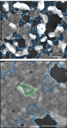
Figure 1: In situ SEM observation of solid-state dewetting on a 40 nm thick silver film on silica held at 330◦C under 400 Pa O2. Blue lines represent the time evolution of the front propagation, the lighter being the older. Green lines represent the grain boundary, the darker being the older. The scale bar is 1 µm.
video 2) suggesting that the dewetting is still not over. In the first studies [8], it was assumed that final particles were formed directly after the isolation of metal domains. Yet a more recent Tranmission Electron Microscopy work high-lighted a film evolution after hole impingement [15], co-herent with our observations. Extraordinary grain growth is another dominant feature of hole propagation in our present study on polycrystalline silver layers on amorphous substrate. It occurs close to the holes but also far away, as observed in iron/sapphire system [7]. For instance, in Fig. 1, the distance from the dewetting front (blue line) to a growing grain isolated on the continuous film (green line) is about 1 µm.
To rationalize these observations, images were analysed to extract the ratio of covered surface, the front length and the number of holes from video 1 (Fig. 2). Although the limit between induction and hole propagation is quite clear [4] i.e the onset of the variation of substrate coverage (marked by a full line in Fig. 2), the transition to sintering calls for a peculiar analysis. In Fig. 2, three events
0 1000 2000 3000 4000 5000 fro nt len gth ( µm ) 0 20 40 60 80 100 % o f co v e re d s u rf a ce a) b) 0 100 200 300 400 500 0 100 200 300 400 500 600 700 800 Nu m be r of ho le s Time (s) c)
Figure 2: a) Covered surface, b) front length and c) number of holes versus time during dewetting of a silver layer at 390◦C under 400 Pa O2. Data obtained from image analysis of video 1 in supplementary materials.
pen simultaneously (marked by a dashed line in Fig. 2) (i) the abrupt change of substrate uncovering rate, (ii) the maximum in front length, (iii) the impingement of holes into a percolated or interconnected domain. This specific time represents the limit when the entire initial layer has been modified by dewetting and when only agglomerated and isolated particles remain. When holes propagate, the front length increases, but on the contrary, it decreases when agglomerated particles sinter. In this state, besides slow Ostwald sintering, intra-particle mass transport is re-quired to change the substrate coverage. This explains the variation of the uncovering rate, even with the same diffu-sion mechanisms. For these reasons, we suggest to define this time point as the global limit between hole propaga-tion and sintering.
As already highlighted, all along the three-step process of dewetting on those polycrystalline layers, grain growth plays a key role. On video 2 of supplementary informa-tion, the image sequence begins shortly before the hole propagation step, at the end of induction time. At this point, grown grains are already observed (see Fig. 3a). Since SEM electron contrast did not allow investigating their formation, the topography and roughness evolution of a 40 nm thick film was monitored during induction
a)
b)
Figure 3: Comparison of two in situ SEM pictures : a) at the be-ginning of hole propagation. The shape of particles present in b) are superposed in green, b) at the beginning of sintering. Zones delim-ited with white lines represent the ensemble of points closer to the particle inside than any other one, the so-called ”zone of influence”. Scale bar is 1 µm.
by AFM. The results are presented in Fig. 4, at differ-ent times a) as deposited, b) after 5 min of annealing at 100◦C, c) after 5 min of annealing at 150◦C. The mean size of grains increases at each annealing treatment, as well as the roughness of the film: 3.9, 4.7, 7.2 nm respec-tively. Between each picture, some grains remained stable, other grains grew; some will go on growing giving birth to hillocks. At the latest stage of induction, although the de-termination may be limited by tip effects, it is possible to find holes with a depth of 20 nm equal to the layer thick-ness which could lead to hole formation, either by thermal grooving [10, 12, 22] or by shrinkage of smaller grains [23]. Unfortunately, the acquisition dynamics did not allow di-rect observation of hole birth. It is important to notice that even if the surface covered by the film is stable, in-duction is far from a static regime. The surface roughness of the film changes drastically and grain shape evolution may be seen as precursory of the next stage. The variety of observed behaviours could result from the absence of any epitaxy on amorphous silica.
At the end of induction time, the layer includes hillocks which appears as large grains, probably silver crystallites,
250 nm (1) (2) (3) g) h) i) 500 nm d) e) f) 1 µm a) b) c) -25 nm +25 nm -50 nm +50 nm
Figure 4: AFM images during induction time: a) as deposited (40 nm layer), b) after 10 min of annealing at 100◦C, c) after 5 min of anneal-ing at 150◦C. Same image during hole propagation in a 20 nm silver layer annealed at 150◦C: d) 6 min, e) 9 min, f) 15 min. SEM images of a 40 nm silver layer annealed in 400 Pa O2at 330◦C: g) reference picture, h) 5 min later, i) relative difference of the two images.
and holes (see Fig. 3-a). The observed morphology is very similar to the one described by Kovalenko et al. during iron on sapphire dewetting [7]. Holes propagate at the same time as hillocks continue growing (see video 2). In the present case, dewetting involve neither the propagation of a rim, nor a succession of growth and shrinkage of touch-ing grains [6, 9]. Dewetttouch-ing results from the propagation of holes, disappearance of small entities and abnormal growth of a limited number of grains. In other words, as already suggested in Ref. [7], a growing grain accumulates mate-rial from the initial layer contained in a ”zone of influence” which can extend up to 1 µm (see Fig. 3b). Moreover, the real-time in situ imaging allows to suggest (thanks to the big number of acquired images) that dewetting front does not propagate along grain boundaries as it was observed on Au/SiOx [15], but whole grains are shrinking instead
(see front propagation in blue lines on Fig.1 or video 2). Complementary AFM topography experiments were per-formed to better understand this issue. Similar morpholo-gies were obtained by AFM upon dewetting in air or in low oxygen pressure in ESEM. Moreover, the mass con-servation as observed through AFM profiles ruled out any sizeable effect of evaporation on the observed phenomena. During hole propagation on a 20 nm silver layer annealed at 150◦C for 6, 9 and 15 min (see Fig. 4, d-f), the grain in the middle of the image is growing in a specific direc-tion corresponding to a given facet (see AFM profiles in supplementary materials). The presence of grain bound-ary seems unlikely, and only a part of the grain is grow-ing. Surface diffusion is governing grain growth, and thus
could be a possible transport path, instead interface dif-fusion and grain boundary sliding as observed in other systems [6, 9],or grain boundary diffusion [7]. As shown in Fig. 3a, the superposition of the shape of the parti-cles just before the beginning of sintering, with the image at the beginning of the hole propagation (Fig.3b) clearly highlights the pre-existence of preferential grains at the end of the induction. Clustering of grains that are to grow into bigger particles are easily identified in this way, which means that very specific grain, growing during induction, will grow further during hole propagation.
During the last sintering step, particles made of several grains tend to transform into single grains. Fig. 4-g,h,i shows the sintering of a particle, initially formed by two grains (g), to a more regular shape (h). As images were taken in exactly the same conditions, the difference be-tween the two pictures reveals qualitatively topology mod-ifications (image difference Fig. 4-i ). It demonstrates that silver has moved from the smaller grain (in dark, marked 1) and allowed the particle growth on specific facets (in light, marked 3). A slight displacement of the particle center of mass was also observed (marked 2), as it is com-monly observed during sintering process.
These real-time SEM measurements shed light on a new description of the dewetting phenomenon in a poly-crystalline layer. Dewetting proceeds in three steps: in-duction, hole propagation and sintering. Each step is deeply governed by grain growth. During induction, spe-cific grains are selected and will accumulate the dewetting silver during the hole propagation step, even far away from the holes; no dewetting rim is observed. Then, a sintering step is observed, during which particles will slowly reach a shape closer to equilibrium. This uncommon dewet-ting scenario, which implies extraordinary grain growth, was already observed for iron but on a different substrate type (single crystal versus amorphous substrate) and in a different environment (reductive versus oxygen atmo-sphere) with other dominating diffusion path (interface versus surface) [7]. The factors governing grain growth and grain selection are still to be understood to explain why these different systems exhibit so similar morphology evolution. Local fluctuations of grain sizes during depo-sition may drive the process but a simple size considera-tion is not sufficient to explain selectivity (Fig.3a). As the substrate herein is amorphous, crystallite epitaxy cannot explain this selection. This point is still under investiga-tion and will probably be a key to understand and control dewetting.
[1] C. V. Thompson, Solid State Dewetting of Thin Films, Annu. Rev. Matter. 42 (2012) 399.
[2] H. Atwater, A. Polman, Plasmonics for improved photovoltaic devices., Nat. mater. 9 (3) (2010) 205–13.
[3] J. Ye, Fabrication of ordered arrays of micro- and nanoscale features with control over their shape and size via templated solid-state dewetting., Sci. Rep. 5 (November 2014) (2015) 9823.
[4] A. Presland, G. Price, D. Trimm, Hillock formation by surface diffusion on thin silver films, Surf. Sci. 29 (2) (1972) 424 – 434. [5] S. K. Sharma, J. Spitz, HILLOCK FORMATION, HOLE GROWTH AND AGGLOMERATION IN THIN SILVER FILMS, Thin Solid Films 65 (1980) 339–350.
[6] A. Kosinova, L. Klinger, O. Kovalenko, E. Rabkin, The role of grain boundary sliding in solid-state dewetting of thin polycrys-talline films, Scripta Mater. 82 (2014) 33–36.
[7] O. Kovalenko, J. Greer, E. Rabkin, Solid-state dewetting of thin iron films on sapphire substrates controlled by grain boundary diffusion, Acta Materialia 61 (2013) 3148–3156.
[8] E. Jiran, C. V. Thompson, Capillary Instabilities in Thin Films films, J. Electron. Mater. 19 (11) (1990) 1153.
[9] A. Kosinova, O. Kovalenko, L. Klinger, E. Rabkin, Mechanisms of solid-state dewetting of thin Au films in different annealing atmospheres, Acta Mater. 83 (2015) 91–101.
[10] R. Dannenberg, E. A. Stach, J. R. Groza, B. J. Dresser, In-situ TEM observations of abnormal grain growth , coarsening , and substrate de-wetting in nanocrystalline Ag thin films, Thin Solid Films 370 (2000) 54–62.
[11] R. Brandon, F. J. Bradshaw, The Mobility of the surface atoms of copper and silver evaporated deposits, Royal Aircraft Estab-lishment, Tech. Rep. (66093).
[12] W. W. Mullins, Theory of Thermal Grooving, J. Appl. Phys. 28 (3) (1957) 333.
[13] L. Klinger, D. Amram, E. Rabkin, Kinetics of a retracting solid film edge: The case of high surface anisotropy, Scripta Mater. 64 (10) (2011) 962–965.
[14] R. V. Zucker, G. H. Kim, W. Craig Carter, C. V. Thompson, A model for solid-state dewetting of a fully-faceted thin film, C. R. Phys. 14 (7) (2013) 564–577.
[15] C. M. M¨uller, R. Spolenak, Microstructure evolution during dewetting in thin Au films, Acta Materialia 58 (2010) 6035– 6045.
[16] G. Atiya, D. Chatain, V. Mikhelashvili, G. Eisenstein, W. D. Kaplan, The role of abnormal grain growth on solid-state dewet-ting kinetics, Acta Mater. 81 (2014) 304–314.
[17] G. Atiya, V. Mikhelashvili, G. Eisenstein, W. D. Kaplan, Solid-state dewetting of Pt on (100) SrTiO3, J. Mater. Sci. 49 (11) (2014) 3863–3874.
[18] F. Niekiel, P. Schweizer, S. M. Kraschewski, B. Butz, E. Spiecker, The process of solid-state dewetting of Au thin films studied by in situ scanning transmission electron microscopy, Acta Mater. 90 (2015) 118–132.
[19] S. Stankic, R. Cortes-Huerto, N. Crivat, D. Demaille, J. Go-niakowski, J. Jupille, Equilibrium shapes of supported silver clusters, Nanoscale 5 (2013) 2448–2453.
[20] G. E. Rhead, SELF-DIFFUSION AND FACETING ON SIL-VER, Acta Metall. 11 (1963) 1035.
[21] R. Podor, D. Pailhon, J. Ravaux, H.-P. Brau, Development of an Integrated Thermocouple for the Accurate Sample Temper-ature Measurement During High TemperTemper-ature Environmental Scanning Electron Microscopy (HT-ESEM) Experiments., Mi-crosc. Microanal. 21 (2) (2015) 307–312.
[22] W. W. Mullins, The effect of grooving on grain boundary mo-tion, Acta Mater. 6 (1958) 414.
[23] V. Derkach, A. Novick-Cohen, A. Vilenkin, E. Rabkin, Grain boundary migration and grooving in thin 3-D systems, Acta Materialia 65 (2014) 194–206.