HAL Id: hal-02334405
https://hal.archives-ouvertes.fr/hal-02334405
Submitted on 26 Oct 2019HAL is a multi-disciplinary open access
archive for the deposit and dissemination of sci-entific research documents, whether they are pub-lished or not. The documents may come from teaching and research institutions in France or abroad, or from public or private research centers.
L’archive ouverte pluridisciplinaire HAL, est destinée au dépôt et à la diffusion de documents scientifiques de niveau recherche, publiés ou non, émanant des établissements d’enseignement et de recherche français ou étrangers, des laboratoires publics ou privés.
Short-circuit robustness of parallel SiC MOSFETs and
fail-safe mode strategy
François Boige, Asad Fayyaz, Alberto Castellazzi, Frédéric Richardeau,
Sébastien Vinnac
To cite this version:
François Boige, Asad Fayyaz, Alberto Castellazzi, Frédéric Richardeau, Sébastien Vinnac. Short-circuit robustness of parallel SiC MOSFETs and fail-safe mode strategy. European Power Elecrtonics and Applications 2019 - IEEE ECCE Europe, Sep 2019, Gênes, Italy. �hal-02334405�
Short-circuit robustness of parallel SiC MOSFETs and fail-safe mode
strategy
François Boige
1, Asad Fayyaz
2, Alberto Castellazzi
2, Frédéric Richardeau
1, Sébastien Vinnac1 1LAPLACE, University of Toulouse, CNRS, France
Tel.: 33 (0) 5 34 32 23 91
2
PEMC Research Group, University of Nottingham, University Park, NG7 2RD, UK
Tel.: 0044 (0) 115 95 15568
E-Mail:
[email protected]; [email protected];
[email protected]; [email protected]
URL:
https://www.nottingham.ac.uk/research/groups/power-electronics-machines-and-control-group/; http://www.laplace.univ-tlse.fr
Keywords
Silicon carbide (SiC), Wide bandgap devices, Power MOSFET, Short-circuit, Robustness, Parallel Operation
Abstract
Silicon carbide (SiC) power MOSFETs exhibit some key differences compared with Silicon (Si) MOSFETs and IGBTs. In particular, both their intrinsic (i.e., material technology related) and extrinsic (i.e., device generation related) features-set implies, on the one hand, higher stress levels of the single chip during a short-circuit and, on the other hand, a greater spread in the value of some of the main electro-thermal parameters affecting the transistor performance during this stressful transient event. Thus, this paper proposes a thorough experimental analysis of the short-circuit robustness of parallel connected SiC Power MOSFETs, taking into account the actual distribution in their parameters. The overall aim is twofold: producing de-rating guidelines for multi-chip structures and developing validated strategies for ensuring new and original soft-fail (or fail-safe) modalities in the application, as a result of both single and repetitive pulse degradation.
Introduction
Silicon Carbide (SiC) power devices exhibit key material properties which lead to some key differences at robustness and system level as compared to Silicon (Si) power devices. Having said that, stressful transient events such as short-circuit are very stressful for SiC Power MOSFETs with really high junction temperature (TJ) and current density. Even though, the SiC Power MOSFET technology is continuously evolving, devices still exhibit a large range of spread in the electro-thermal device parameters namely: threshold voltage (Vth), on-state resistance (RDS(ON)) and trans-conductance (gm) etc. TJ unbalance may also arise due to other factors relating to circuit layout and non-linearity with cooling etc. [1, 2]. A stressful event like short-circuit could be critical when paralleling chips as significant unbalance in TJ between devices could lead to premature failure of the complete module and hence motivated this study.
Analysis of device parameter spread: Static measurements
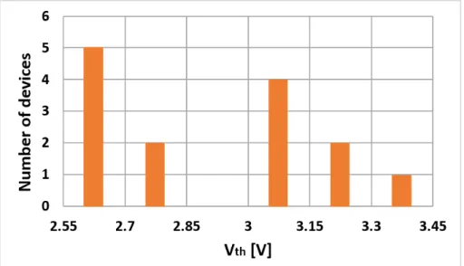
The study presented in this paper focuses on two similar rating device types from two different manufacturers. The device referred to as Dev-A [3] is a 1200 V, 80 mΩ, 36 A rated power MOSFET whereas Dev-B [4] is a 1200 V, 80 mΩ, 41 A rated device. For the sake of illustration, Fig. 1 shows the typical distribution of measured Vth on a number of Dev-B commercial devices. In here, it can be clearly seen that the spread could be quite broad (in this case, the range is: 2.55 V – 3.45 V) as much as approximately 1 V at case temperature (TCASE) of 25 oC (i.e. room temperature). A similar ΔVth spread
of around 1 V as presented in Fig. 1 was also observed for Dev-A device type with a range of 3.02 V – 4.03V. However, the measured Vth values for both device types still have a good correlation with datasheet and the measured values fall within the minimum and maximum value defined by the datasheet. Here, Vth was defined as the gate source voltage (VGS) value at which the drain current (ID) was 5 mA when VDS = VGS where VDS is the drain source voltage. At the same time, Vth over a range of TCASE was also measured and ΔVth was found to get bigger as the temperature was increased. Fig. 2 represents the Vth behaviour for two Dev-B devices under test (DUTs) over a TCASE range of 25 oC – 150 oC. Here, for TCASE = 25 oC, ΔVth is 265 mV and for TCASE = 150 oC, ΔVth is 450 mV. Lastly, the measured RDS(ON) for the DUTs also ranged between 79 mΩ – 84 mΩ.
Fig. 1. Distribution of measured Vth spread for Dev-B DUT showing ΔVth of app. 1 V (Datasheet min. 2V and max. 4V) at TCASE = 300 K
Fig. 2. Variation of Vth for two Dev-B DUTs over TCASE between 25 oC and 150 oC
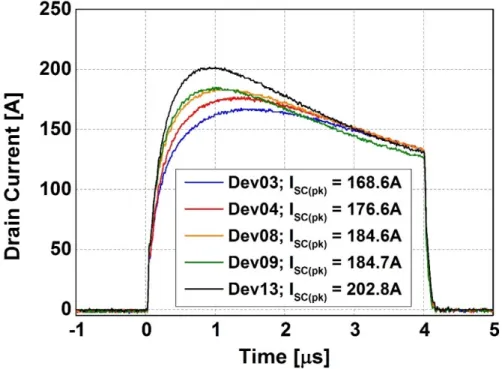
Short-circuit (SC) withstand capability is an important requirement in many applications such as: motor drive applications. Even-though, SC event is typically unintentional but nonetheless can be a frequent event and is usually perceived to be very stressful for the device. To demonstrate the implication of the device parameter spread on the electro-thermal stress during SC, tests were performed on devices with different Vth values. Fig. 3 shows the difference in the peak drain current (ID(pk)) for Dev-B DUTs which is around 35 A as a result of the given device parameter spread investigated. The device with lower Vth would result in higher ID(pk) and vice versa. When comparing two DUTs (same device type) with far
apart Vth, DUT with higher Vth is referred to as a strong device (due to lower ID(pk) and thus lower resulting TJ) and a DUT with a lower Vth is referred to as a weak device (due to higher ID(pk) and thus higher resulting TJ). These tests were carried out with VDD = 600 V, VGS = 18 V and TCASE = 25 oC. The resultant TJ profile for the SC results presented in Fig. 3 were also simulated using an equivalent physical thermal model (explained in more detail in [5]) are subsequently presented in Fig. 4. Here, maximum junction temperature (TJ(max)) for these tests was around 570 oC and the ΔTJ(max) is around 30 oC. Such difference in TJ as a result of device parameter spread can be critical from a reliability and robustness point of view. More importantly, single pulse as well as repetitive stress aging are also of concern.
Fig. 3. VDS = 600 V, TCASE = 25 oC and VGS = 18 V; SC Experimental waveforms for Dev-B DUTs; Vth range between 2.55 V (Dev13) and 3.45 V (Dev03)
Fig. 4. Corresponding simulated TJ(max) estimation for SC waveforms in Fig. 3
It is typically very difficult, if not impossible, to predict how a given set of device characteristics will evolve over time due to stress and so, ultimately, to predict when a device will fail. Therefore, in order to establish suitable de-rating criteria for a given target operational lifetime, it is important to also develop strategies to monitor degradation and impeding failure and respond in a way which ensures
soft-fail and non-propagation of the failure at system level [6, 7]. In this context, soft-fail or fail-safe mode happens when the DUT fails as a result of a short between gate-source which eventually results in measureable residual gate-source resistance (RGS) of tens of ohms which is usually defined as the drain-source fail-to-open failure mode. Ensuring such kind of failure mode is favourable not only for the system’s safety in general, but also avoids catastrophic failure of the DUT and subsequent physical damage to the surrounding components.
Experimental SC test results: Parallel connected DUTs
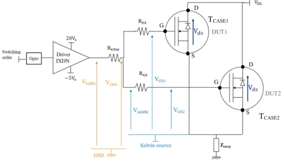
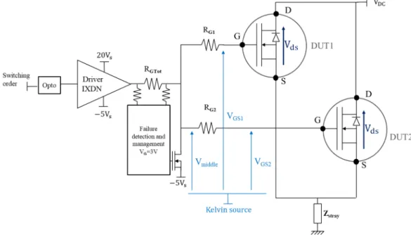
This section represents the experimental SC results performed on two parallel connected DUTs of the same device type (i.e. same part number). Such parallel connection test analysis was performed for two different DUT types from two different manufacturers; Dev-A and Dev-B. Here, the idea was to perform SC tests with an aim of obtaining a soft-fail (drain-source fail-to-open) criteria [8]. Therefore, depending on previous device characterisation of the DUTs as also included in [8, 9], the input voltage (VDD) was appropriately adjusted to ensure soft-fail mode at all times. The gate driver circuit schematic which was implemented to perform these tests is presented in Fig. 5 below. The gate drive voltage (Vbuffer) was switched between +20/-5V. The buffer IC has a 14 A peak current capability with a rise and fall time of less than 30 ns.
Fig. 5. Circuit schematic of the implemented gate drive network
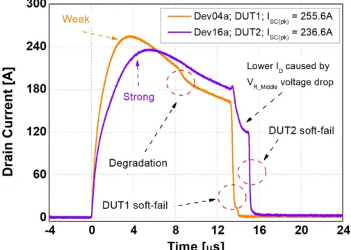
The first results presented here, are on two parallel connected Dev-A device type with ΔVth of 1 V. These results were carried out with VDD = 600 V, VGS = +20/-5 V, TCASE1 = TCASE2 = 25 oC. Here, the total gate resistance (RGTot) is the common used gate resistance for the total gate loop current (IG) whereas the separate RG1 and RG2 were also used. In this case, the resistor values used were as follows: RGTot = 10 Ω and RG1 = RG2 = 27 Ω. Since Dev-A DUT undergoes a soft-fail mode during SC [8] with applied input bias of 600 V, therefore, this value was used for these tests presented here. Moreover, it represents 50% of the rated breakdown voltage (VBD(DSS)) and usually devices are de-rated at 50%. Therefore, to have a SiC device which can withstand 10 µs with 50% voltage de-rating and at the same time has a soft-fail SC failure mode does indeed represent a useful consideration feature when developing power systems using SiC devices. Here, a SC pulse with duration (tSC) of 30 µs was sent to both DUTs to trigger the failure and to be able to investigate if there is any extra margin on SC withstand capability for the device with lower ID(pk) (i.e. strong device – higher Vth) prior to failure. Fig. 6 shows the SC waveforms for the two DUTs in question. Here, it is very interesting to see that if the device spread is big enough (ΔV 1V), the device with higher ID(pk) (i.e. weak device – lower Vth) fails first and then the strong device failed 1.8 µs afterwards. The failure tSC observed was 13.2 µs and 15.0 µs for DUT1 (weak) and DUT2 (strong) device respectively. It has to be noted that DUT2 is degraded around
TCASE1
8µs which results in a gate leakage current but the device continues to support the short-circuit up to 13µs. Another important point to iterate here is that this type of device (Dev-A) can sustain tSC > 10 µs at 50% of VBD(DSS). The corresponding VGS waveforms for the SC current waveforms presented in Fig. 6 are subsequently presented in Fig. 7. As presented in Fig. 7, the failure of each DUT in gate-source fail-to-short was also confirmed as the VGS for DUT1 and DUT2 decreased to a value very close to zero subsequently. The measured residual RGS for DUT1 and DUT2 was 2.6 Ω and 3.6 Ω respectively. The lower ID for DUT2 just before failure is actually due to the potential drop at Vmiddle due to increased gate leakage current in DUT1 when it failed. Indeed, once the weak device fails, VGS1 = 0 V leading to the voltage drop of Vmiddle caused by the voltage divider composed of RGTot and RG2.
Fig. 6. Drain Current (ID) waveforms; Dev-A VDD = 600 V; VGS = +20/-5 V; TCASE1 = TCASE2 = 25 oC; DUT1 – Dev04a – Weak – Vth = 3.0 V (Orange); DUT2 – Dev16a – Strong – Vth = 4.0 V (Purple)
Fig. 7. Gate-source voltage (VGS) waveforms corresponding to ID in Fig. 6; Dev-A DUT1 – Dev4a – Vth = 3 V (Orange); DUT2 – Dev16a – Vth = 4 V (Purple); Vmiddle (Green)
Furthermore, results on Dev-B device are also presented here. For this type of device, VDD was set to 250 V to ensure soft-fail (short between gate-source) mode for this particular device which is only possible at relatively lower VDD (i.e. lower power) [9]. In this case, the distributed gate resistor values were decreased to the lowest acceptable value to avoid ringing (RG1 = RG2 = 5 Ω). The aim is to naturally turn-off the stronger DUT when the weak one fails. To do so, the distributed gate resistors have to be as low as possible to pull down the strong device’s gate voltage below the threshold voltage. Fig. 8 shows the ID waveforms for two parallel-connected Dev-B DUTs.
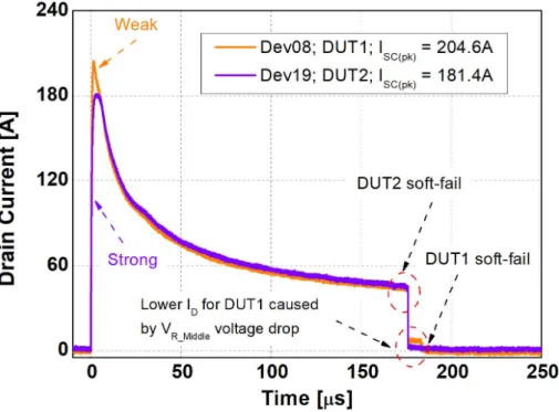
Fig. 8. Drain Current (ID) waveforms, Dev-B; VDD = 250 V; VGS = +20/-5 V; TCASE1 = TCASE2 = 25 oC; DUT1 – Dev08 – Weak – Vth = 2.5 V (Orange); DUT2 – Dev19 – Strong – Vth = 3.1 V (Purple)
Fig. 9. Gate-source voltage (VGS) waveforms corresponding to ID in Fig. 8; Dev-B DUT1 – Dev08 – Vth = 2.5 V (Orange); DUT2 – Dev19 – Vth = 3.1 V (Purple); Vmiddle (Green)
A very long pulse of 260 µs was sent to the DUTs and as can be seen, the ID current decreased to zero (gate-source short) at failure. Here, DUT2 and DUT1 failed at around 174 µs and 184 µs respectively. Unlike the case of Dev-A, device type Dev-B DUT with the lower Vth (DUT1) failed afterwards. It is due to the fact that the saturation current of the device with the higher Vth (DUT2) is slightly higher after the transient peak at the start of the short-circuit, as seen in Fig. 8. This higher saturation current leads to a slightly higher TJ(max) hence an earlier failure. Here, the failure mode is highly dependent on temperature [8, 9]. The failure could also be confirmed by the gate drive waveforms, which also decrease to zero at failure indicting that the device has failed with a very low value residual RGS, which in this case was measured to be roughly 0.2 Ω for both DUTs. Fig. 9 shows the gate drive waveforms for the two DUTs. From Fig. 9, it is clear that DUT1 fails around 10 µs afterwards when the VGS (orange waveform) subsequently drops to zero. The extremely low ID for Dev08 just before failure is actually due to the high potential drop at Vmiddle due to the low RG1,2 and high RGTot. It can also be noted that this potential is very close to the device’s threshold voltage but not small enough to completely turn-off the device.
SC Protection Circuitry
Starting from the observation that whatever the set of gate resistors, in the case of a long short-circuit, the drop in VGS caused by the failure of the weaker device does not automatically turn-off the other device, especially since RG1,2 had a minimum value of 5 Ω to avoid ringing. To ensure that the other device is turned-off when the weak device fails, a protection circuit was integrated close to the gate driver. The protection circuit, whose electronics will not be detailed in this article, ensures soft shutdown (SSD) of the strong device when the failure of the weak device occurs. Basically, when an important voltage drop is measured across RGTot (3 V), a low voltage transistor is turned on to pull down Vmiddle at -5 V to turn off the remaining DUT. The low voltage transistor is turned on slowly in order to softly turn off the DUT in short-circuit condition and avoid unnecessary stress. The test circuit with protection is shown in Fig. 10. Tests similar to those presented in the previous section were performed with Dev-A at 600 V and Dev-B DUT at 200 V.
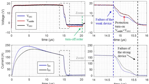
Fig. 10. Circuit schematic of the implemented gate drive network and the gate protection circuit A short-circuit test with Dev-A DUT and the protection circuit was performed at VDS = 600 V and ΔVGS(th) = 1 V similar to the test without protection circuit as presented in previous section. The test results are shown in Fig. 11. The device with the lower threshold voltage fails first at 14.7 µs and the protection circuitry reacts (Vmiddle = VGS2). After a very short time after turn-off, the second device fails at 15.5 µs, there is a dissociation between the voltage Vmiddle and VGS2 indicating a breakdown of the gate
of DUT2 (Vmiddle ≠ VGS2 = VGS1). At the end, Vmiddle = -5 V corresponding to the potential to which the transistor is connected to perform the SSD. For Dev-A DUT, even with a very large Vth difference, the strongest DUT cannot be saved. A short-circuit test with the Dev-B DUT and the protection circuit was performed at VDS = 200 V and ΔVth = 400 mV similar to the test without protection circuit as included in previous section. The test results are presented in Fig. 12, as for the test in Fig. 8 and 9, the DUT with the higher Vth fails first at 157.5 µs because, on average, its saturation current is slightly higher, so it has slightly higher TJ(max). This confirms the previous results and indicates that in the case of long SC pulses with low power density, other parameters apart from Vth also influence the saturation current. Here. the protection circuit reacts as soon as the strong device fails, the second DUT is turned-off and does not fail afterwards. In this case, the protection circuit managed to save the weak device.
Fig. 11. Gate-source voltage (VGS) and Drain Current (ID) waveforms; Dev-A; VDS = 600 V; VGS = +20/-5 V; TCASE1 = TCASE2 = 25 oC; RGTot = 10 Ω; RG1 = RG2 = 27 Ω; DUT1 – Dev02a – Weak – Vth = 3.0 V (Blue); DUT2 – Dev17a – Strong – Vth = 4.0 V (Black)
Fig. 12. Gate-source voltage (VGS) and Drain Current (ID) waveforms; Dev-B;
VDS = 200V; VGS = +20/-5V; TCASE1 = TCASE2 = 25 oC; RGTot = 27 Ω, RG1 = RG2 = 5 Ω; DUT1 – Dev18 – Weak – Vth = 2.5 V (Blue); DUT2 – Dev10 – Strong – Vth = 3.1 V (Black); Vmiddle (Green)
Conclusion
SC experimental case study in soft-failure mode has been presented on the parallel connected DUTs representative of a multi-chip structure within a power module. The chosen DUTs are known to have fail-to-open drain-source failure mode (i.e., short-circuit gate-source) allowing the chips in the module to still be usable even if one of them fails and avoiding the quick high-energy discharge of any capacitors into the circuit. However, this condition is only satisfied, for most devices, at relatively low values of VDS: only one commercial device has been identified, which fails to soft in SC even with VDS = 600 V (i.e., 50% of the nominal rating). This paper focused on trying to relate some device parameter and its spread (e.g., Vth) to their SC withstand capability and the impact of the soft failure mode of one of device on another connected in parallel, specifically to assess the possibility to save it.
For Dev-A device, it is seen that if a large spread in Vth exists, then the device with lower stress (typically, the one with higher Vth) can sustain longer SC times, as a result of lower power dissipation and slower rising junction temperature during the pulse. However, in the case of Dev-B devices with low power dissipation and long short-circuit time, the Vth spread is not the only parameter which has an impact on the device’s junction temperature. Here, he RDS(ON) of the device also plays a role since the SC duration is relatively long. For Dev-B DUT, the gate failure due to a gate-source short of the first failed device tends to lower the gate bias of the other device. This mechanism lowers the saturation current and enhances the SC withstand time of the remaining device in parallel. An investigation has been conducted to evaluate if this mechanism could be used to automatically turn-off all the remaining devices in parallel (without the need of protection circuitry) within a module: that was not achieved in this study, due to the minimum gate-resistance values needed to avoid ringing in the setup. To overcome the problem of ringing with gate resistors close to 0 Ω, a custom developed protection circuit has been added to the setup to act as the perfect gate resistor set-up. Indeed, the protection circuit detects the gate failure and turn-off the device which survived. Even with an “ideal” resistor set-up, the difference in SC time caused by the parameter spread has to be long enough (few µs) to safely turn-off the strong device. It is therefore possible that during the failure of the weak chip in "fail-to-open drain-source" the protection circuit also causes the remaining devices in the module to be turned-off.
As a perspective, after the turn-off, some of the chips inside the module are still functional. In order to restart the system, the disconnection of the defective chip(s) is mandatory because the low gate-source residual resistance of the failed device decreases the gate bias for the remaining chips, affecting their performance with increased system losses. It is therefore interesting, in the future, to explore ways of disconnecting the gate of the failed chips in a module configuration to always ensure fail-safe mode strategies.
References
[1] Castellazzi, Alberto, Asad Fayyaz, and Rainer Kraus. "SiC MOSFET device parameter spread and ruggedness of parallel multichip structures." In Materials Science Forum, vol. 924, pp. 811-817. Trans Tech Publications, 2018.
[2] Li, Helong, Stig Munk-Nielsen, Xiongfei Wang, Ramkrishan Maheshwari, Szymon Bęczkowski, Christian
Uhrenfeldt, and W-Toke Franke. "Influences of device and circuit mismatches on paralleling silicon carbide MOSFETs." IEEE Transactions on Power Electronics 31, no. 1 (2016): 621-634.
[3] Microsemi, "APT40SM120B Datasheet." [4] Wolfspeed, "C2M0080120D Datasheet."
[5] Fayyaz, Asad, Li Yang, and Alberto Castellazzi. "Transient robustness testing of silicon carbide (SiC) power
MOSFETs." In 2013 15th European Conference on Power Electronics and Applications (EPE), pp. 1-10. IEEE, 2013.
[6] Riccio, M., A. Borghese, G. Romano, V. d'Alessandro, A. Fayyaz, A. Castellazzi, L. Maresca, G. Breglio, and
A. Irace. "Analysis of Device and Circuit Parameters Variability in SiC MOSFETs-Based Multichip Power Module." In 2018 20th European Conference on Power Electronics and Applications (EPE'18 ECCE
Europe), pp. P-1. IEEE, 2018.
[7] Borghese, Alessandro, Antonio Pio Catalano, Michele Riccio, Lorenzo Codecasa, Asad Fayyaz, Vincenzo d’Alessandro, Alberto Castellazzi, Luca Maresca, Giovanni Breglio and Andrea Irace. "An Efficient Simulation Methodology to Quantify the Impact of Parameter Fluctuations on the Electrothermal Behavior of
Multichip SiC Power Modules." In Materials Science Forum, vol. xx, pp. xxx-xxx. Trans Tech Publications, 2019. (In press)
[8] Boige, François, Frédéric Richardeau, S. Lefebvre, J-M. Blaquière, G. Guibaud, and Abdelhakim Bourennane.
"Ensure an original and safe “fail-to-open” mode in planar and trench power SiC MOSFET devices in extreme short-circuit operation." Microelectronics Reliability 88 (2018): 598-603.
[9] Romano, Gianpaolo, Asad Fayyaz, Michele Riccio, Luca Maresca, Giovanni Breglio, Alberto Castellazzi, and
Andrea Irace. "A comprehensive study of short-circuit ruggedness of silicon carbide power MOSFETs." IEEE