HAL Id: hal-02267956
https://hal.archives-ouvertes.fr/hal-02267956
Submitted on 7 Oct 2020
HAL is a multi-disciplinary open access
archive for the deposit and dissemination of
sci-entific research documents, whether they are
pub-lished or not. The documents may come from
teaching and research institutions in France or
abroad, or from public or private research centers.
L’archive ouverte pluridisciplinaire HAL, est
destinée au dépôt et à la diffusion de documents
scientifiques de niveau recherche, publiés ou non,
émanant des établissements d’enseignement et de
recherche français ou étrangers, des laboratoires
publics ou privés.
Electronic coupling in the F4-TCNQ/single-layer GaSe
heterostructure
Lama Khalil, Debora Pierucci, Evangelos Papalazarou, Julien Chaste,
Mathieu Silly, Fausto Sirotti, Mahmoud Eddrief, Luca Perfetti, Emmanuel
Lhuillier, Abdelkarim Ouerghi
To cite this version:
Lama Khalil, Debora Pierucci, Evangelos Papalazarou, Julien Chaste, Mathieu Silly, et al.. Electronic
coupling in the F4-TCNQ/single-layer GaSe heterostructure. Physical Review Materials, American
Physical Society, 2019, 3 (8), �10.1103/PhysRevMaterials.3.084002�. �hal-02267956�
Electronic coupling in the F4-TCNQ/single layer GaSe heterostructure
Lama Khalil*1, Debora Pierucci2, Evangelos Papalazarou3, Julien Chaste1, Mathieu G. Silly4, Fausto Sirotti5,
Mahmoud Eddrief6,7, Luca Perfetti8, Emmanuel Lhuillier9, and Abdelkarim Ouerghi*1
1Centre de Nanosciences et de Nanotechnologies, CNRS, Univ. Paris-Sud, Université Paris-Saclay, C2N –
Palaiseau, 91120 Palaiseau, France
2CELLS - ALBA Synchrotron Radiation Facility, Carrer de la Llum 2-26, 08290 Cerdanyola del Valles,
Barcelona, Spain
3Laboratoire de Physique de Solides, CNRS, Univ. Paris-Sud, Université Paris-Saclay, 91405 Orsay Cedex,
France
4Synchrotron SOLEIL, Saint-Aubin BP 48, Gif-sur-Yvette F-91192, France
5Laboratoire de Physique de la Matière Condensée, CNRS – Ecole Polytechnique, 91128 Palaiseau cedex,
France
6Sorbonne Universités, UPMC Université Paris 06, UMR 7588, INSP, F-75005 Paris, France 7CNRS, UMR 7588, Institut des Nanosciences de Paris (INSP), F-75005 Paris, France
8Laboratoire des Solides Irradiés, Ecole Polytechnique, CNRS, CEA, Université Paris-Saclay, 91128 Palaiseau
Cedex, France
9Sorbonne Université, CNRS, Institut des NanoSciences de Paris, INSP, F-75005 Paris, France
Hybrid heterostructures, made of organic molecules adsorbed on two-dimensional metal monochalcogenide, generally unveil interfacial effects that improve the electronic properties of the single constitutive layers. Here, we investigate the interfacial electronic characteristics of the F4-TCNQ/single layer GaSe heterostructure. A sharp F4-TCNQ/GaSe interface has been obtained and characterized by X-ray photoemission spectroscopy. We demonstrate that a high electron transfer from 1TL GaSe into the adsorbed F4-TCNQ molecules takes place, thereby yielding a reduction in the excess negative charge density of GaSe. Additionally, the direct band structure determination of the heterostructure has been carried out using angle-resolved photoemission spectroscopy, shedding light on essential features such as doping and band offset at the interface. Our results indicate that the buried 1TL GaSe bellow the F4-TCNQ layer exhibits a robust inversion of the valence dispersion at the Γ point, forming a Mexican-hat-shaped dispersion with 120 ± 10 meV of depth. Our experiments also reveal that F4-TCNQ can significantly tune the electronic properties of 1TL GaSe by shifting the band offset of about 0.16 eV toward lower binding energies with respect to the Fermi level, which is a key feature for envisioning its applications in nanoelectronics.
Keywords: Gallium Selenide – tetrafluorotetracyanoquinodimethane – ARPES – Electronic band structure – Charge transfer
Since the successful mechanical exfoliation of graphene1—a monolayer of carbon atoms with high carrier mobility,
two-dimensional (2D) layered materials have received the attention of a large area of the scientific community thanks to their emergent optical and electrical properties. In particular, 2D metal monochalcogenides MX (M =
Ga, In; X = Se, Te, S) are considered highly promising candidates for a new generation of electronic and optoelectronic devices.2–5 However, unlike graphene, which does not exhibit a band gap preventing its potential
optoelectronic applications, these 2D compounds present a band gap. Particularly, gallium selenide GaSe is gaining an original interest due to its indirect-to-direct band gap transition when moving from single- to approximatively seven-layer structure.6,7 From here comes the significant importance of studying the effects of
combining graphene layers with 2D semiconducting MX systems like GaSe, in a van der Waals (vdW) heterostructure, in order to merge the numerous interesting properties of these materials with the high electron and hole mobility of graphene.8 This 2D materials/graphene-based technology is expected to provide an exciting
avenue to engineer novel devices used as highly responsive photodetectors.
GaSe belongs to the family of semiconductor crystals made of stacked layers in units of Se-Ga-Ga-Se, which form an atomic tetralayer (TL); bonding between atomic planes within a TL is covalent, whereas bonding between adjacent fourfold layers is predominantly of the weak ionic and vdW type. Bulk GaSe has a direct band gap of about 2 eV and shows a p-type transport behavior.9,10 Moreover, GaSe has been extensively employed as a
photoconductor,11 a second harmonic generation crystal in nonlinear optics,12 and a far-infrared conversion
material.13 More recently, it has been investigated in its 2D layered form,7,14 where tuning of its band gap by
varying the film thickness has been demonstrated, making this compound suitable for vdW heterostructures such as light-emitting diodes.15 To stimulate the growth of large areas of 2D crystals of GaSe on graphene for device
fabrication, the epitaxial growth of TLs of GaSe films seems to be one of the most appropriate synthetization techniques. Recently, we have demonstrated the successful epitaxial growth of GaSe on graphene.7,16 In particular,
1TL GaSe/graphene is ntype doped, exhibiting a valence band maximum (VBM) at a binding energy (BE) of -2.3 eV and a band gap of about 3.5 eV.7 In this respect, functionalizing GaSe/graphene heterostructure with the
strong electron acceptor tetrafluorotetracyanoquinodimethane, abbreviated as F4-TCNQ, is a very promising approach to tune the doping of this system and exploit the unique properties that could derive from the interplay between these atomically thin GaSe materials on graphene with organic molecules. It has already been demonstrated that F4-TCNQ molecules have been extensively employed in organic light emitting diodes to improve the hole-injection barrier, which significantly enhance the efficiency and the performance of these devices.17–22 Detailed investigations have also confirmed that these molecules can be successfully used as a state
of the art p-type dopant in carbon nanotubes23–25 and graphene.26–28 In parallel, first-principles theoretical
calculations have anticipated that hole doping of mono- and multi-layer GaSe, is at the heart of unusual physics, and could induce a high density of states (DOS) and a van Hove singularity quite close to the VBM.29 This hole
doping process of 2D crystals of GaSe may thus offer many intriguing results for possible ferromagnetic phase transitions, and could be achieved for instance by using F4-TCNQ molecules since they are generally used as a p-type dopant to enhance the hole conductivity in several devices.
In order to shed light on the electronic effects of F4-TCNQ molecular incorporation on the surface of single TL GaSe, we performed in the present work a photoemission study via X-ray photoemission spectroscopy (XPS) and angle-resolved photoemission spectroscopy (ARPES). The combination of these techniques gives access to the information on how the molecular doping procedure affects the electronic properties of the 1TL GaSe/graphene heterostructure (i.e., charge transfer, band structure, etc.). Thanks to the energy resolution, our results indicate that
the n-type doping of 1TL GaSe/graphene can be tuned by F4-TCNQ functionalization. Particularly, we demonstrate that the overall electronic band structure of 1TL GaSe is preserved and rigidly upshifts toward the Fermi level.
Experimental details:
1TL GaSe was directly grown on bilayer graphene/SiC(0001) by molecular beam epitaxy (MBE) under ultrahigh vacuum (UHV) conditions (base pressure of 5 × 10⁻¹⁰ mbar) to avoid contamination that could be introduced by
chemical transfer.30 Elemental gallium (Ga) of 99.99% purity and selenium (Se) of 99.99% purity were employed
as the sources, and their fluxes were produced from a Knusden cell. During the film deposition, the substrate was kept at about 350°C. A typical growth rate of about 1.5 nm/min was used; this value was determined by means of scanning transmission electron microscopy (STEM) technique.7 The growth was monitored in situ by reflection
high-energy electron diffraction (RHEED),16 which showed streaky patterns, revealing the 2D growth mode of
GaSe. This vdW epitaxy permits the combination of 2D layered materials even though they present a large lattice mismatch.7,16,31,32 After the growth, a Se capping layer was deposited on the top of the samples to protect them
from oxidation and contamination. This capping layer was then removed, in order to perform the photoemission measurements, by annealing the samples at 250°C in UHV for 40 min. Subsequently, F4-TCNQ molecules (Sigma-Aldrich, 99% purity) were evaporated on the 1TL GaSe/graphene heterostructures from a well outgassed heated crucible, keeping the sample at room temperature; the evaporation rate was about 0.18 Å/min for 15 min.
The electronic properties of the F4-TCNQ/1TL GaSe heterostructures were probed using XPS and ARPES techniques. The experiments were performed at room temperature on the TEMPO beamline at the SOLEIL synchrotron light source. The photon source was a HU80 Apple II undulator set to deliver horizontally linearly polarized light. The energy of photons was selected using a high-resolution plane grating monochromator, with a resolving power E/ΔE that can reach 15 000 on the whole energy range (45 – 1500 eV). During the XPS measurements, the photoelectrons were detected at normal emission angle and at 46° from the polarization vector. The spot size was 100 × 80 (H × V) µm2.
Results and discussion:
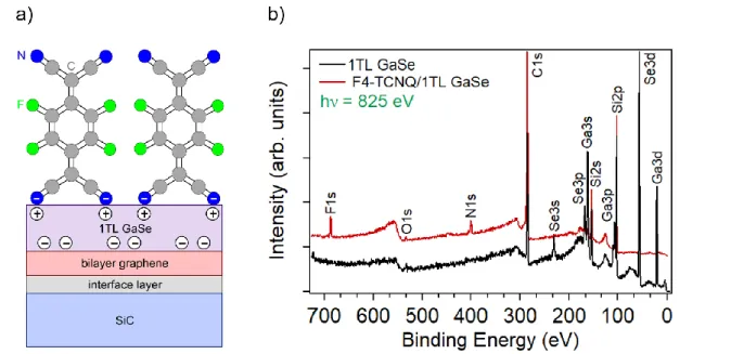
In Figure 1a, we exhibit a schematic view of the F4-TCNQ molecular layer deposited on top single TL GaSe grown on bilayer graphene/SiC(0001) substrate. To investigate quantitatively the elemental composition and its chemical environment of our samples, XPS measurements have been performed for pristine and molecular doped 1TL GaSe. Figure 1b shows representative wide XPS spectra before and after F4-TCNQ deposition, acquired using photons with an energy of 825 eV. By comparing the core level photoemission yields of clean and doped specimens, we can clearly detect the presence of two additional peaks, namely, the F 1s and N 1s core levels, and an increase in the photoemission intensity of the C 1s peak for the doped sample with respect to the pristine one, indicating the successful F4-TCNQ coverage of 1TL GaSe.
High resolution core level photoemission spectra for Ga 3d (Figures 2a and 2b), N 1s (Figure 2c) and F 1s (Figure 2d), taken on both 1TL GaSe (black circles) and F4-TCNQ/1TL GaSe (red circles), were also recorded at photon energies of 60 eV (Ga 3d) and 825 eV (N 1s and F 1s). The experimental data points are represented as black and
red circles, the envelope of fitted components is shown as a blue solid line, and the fitting components of the Ga
3d and N 1s XPS spectrum are plotted as orange curves. In Figures 2a and 2b, we compare core level photoemission
spectra of Ga 3dobtained before and after molecular deposition. The Ga 3d spectra can be deconvoluted using two components corresponding to Ga 3d5/2 and Ga 3d3/2 (spin-orbit splitting of 0.45 eV, 3d3/2:3d5/2 ratio of 0.66 and
full width at half maximum FWHM = 0.7 eV).33 In the pristine sample, the BE of Ga 3d
5/2 is 20.05 eV, which
evolves to 19.89 eV after molecular coverage. Therefore, a rigid shift of 0.16 eV towards lower binding energies is obtained upon F4-TCNQ adsorption. This downshift can be attributed to an interfacial electron transfer from 1TL GaSe into the adsorbed F4-TCNQ molecules, possessing a high electron-accepting character,22,34 which
reduces the excess n-type doping previously induced by graphene.7 It is worth noting that no additional components
were present in the Ga 3d spectra. These observations confirm that there were no covalent bonds formed between F4-TCNQ and GaSe, which indicates that a sharp F4-TCNQ/GaSe interface has been obtained.Moreover, N 1s and F 1s core level emission spectra are also displayed in panels c and d of Figure 2, respectively. To fit the XPS experimental data of the N 1s core level, three components centered at BEs of 398.4 eV, 400.2 eV and 401.2 eV were required (FWHM = 1.7 eV). This shows the presence of different N species in the adsorbed molecular layer. As found in preceding studies,27,28,35 the first component located at 398.4 eV can be attributed to N-1 anionic species
of the negatively charged F4-TCNQ in direct contact with 1TL GaSe, while the second one at 400.2 eV can be assigned to the N0 neutral species of bulk F4-TCNQ. The additional higher BE component at 401.2 eV can be
related to shake up processes.36 The presence of the N-1 anion species reflects that the charge transfer process
occurs through the C≡N groups of the F4-TCNQ molecules, which extract electrons from GaSe,37 while the
fluorine atoms remain inactive. In fact, the lineshape analysis of the F 1s spectrum (panel 2d) reveals only a single component centered at a binding energy of 687.1 eV (FWHM = 2.17 eV). Nevertheless, only 63% of the C≡N groups are implicated in the charge transfer process (i.e., 37% of the C≡N groups remain uncharged), as determined from the peak area ratios of the fitted components. This indicates that the F4-TCNQ molecules are not perfectly flat on the GaSe surface. Actually, a possible standing up configuration can be present, exposing only parts of the C≡N groups in contact with GaSe.28
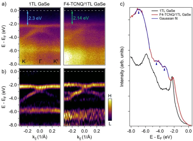
Further insight into the effect of this charge transfer process on the electronic band structure of GaSe was obtained using ARPES. In Figure 3a, we compare photoelectron intensity maps, acquired with a photon energy of 60 eV along the GaSe ΓK-ΓK’ high symmetry direction, revealing the evolution of the electronic structure of 1TL GaSe upon F4-TCNQ adsorption. In order to enhance fine spectral features and get better clarity of the band structure presented in Figure 3a, the second derivatives of the photoelectron intensity as a function of BE and parallel wave vector were also provided in Figure 3b. As can be seen in the left panel of Figure 3a, right before any molecular adsorption, one can notice the Mexican-hat-shaped electronic energy dispersion with 120 ± 10 meV of depth as a typical signature of the single-layered GaSe. This particular shape gives rise to a high DOS, which creates a van Hove singularity in the proximity of the VBM. Moreover, as already discussed in previous studies on few-layer GaSe,7,32 we can evidently notice that the VBM of 1TL GaSe is not located at the Γ point, in contrast to GaSe
bulk,16 due to quantum confinement. Moving to the right panel of Figure 3a, we remark that, as in the left panel,
F4-TCNQ/1TL GaSe also exhibits a robust inversion of the valence dispersion at the Γ point, forming a Mexican-hat-shaped dispersion. Besides, the F4-TCNQ coverage initially results in a blurring of the 1TL GaSe electronic states. To better visualize the difference between the two ARPES images and make the comparison quite effective,
we have included energy distribution curves (see Figure 3c) extracted by integrating the spectra in Figure 3a. After doping the interface with molecules, some almost prominent dispersionless photoemission features markedly arise, centered at 3.36 ± 0.02 eV, 4.47 ± 0.06 eV and 6.94 ± 0.01 eV BE (these values are extracted by fitting the data with a Gaussian function as shown in Figure 3c). These various new features can be assigned to several frontier orbitals of F4-TCNQ and to F4-TCNQ/1TL GaSe interface states. In particular, the broad component centered at 3.36 eV can be unambiguously attributed to the highest occupied molecular orbital (HOMO) state of F4-TCNQ, consistent with a previous study on hydrogenated diamond.37 In addition, after adding molecules on the surface of
1TL GaSe, the overall electronic structure rigidly shifts of about 0.16 eV towards the Femi energy, i.e., towards lower BEs, with respect to the pristine sample: particularly, the VBM located at about -0.2 Å-1 corresponds to a
BE of -2.3 ± 0.01 eV and -2.14 ± 0.01 eV for 1TL GaSe and F4-TCNQ/1TL GaSe, respectively. This energy shift is the same as the one obtained for the core levels of Ga 3d, confirming that a surface transfer, which decreases the n-type doping of 1TL GaSe, has occurred. The fact that charge transfer takes place in a low density of in-gap states can explain the reason why the LUMO resides bellow the Fermi level also after the charge transfer.40,41Additional in-gap states have been already detected in systems where F4-TCNQ forms a charge
transfer complex with various organic and inorganic components38,39. These states are related to the partially filled
lowest unoccupied molecular orbitals (LUMO’) and to the relaxed HOMO (HOMO’) of the anion molecules at the interface upon the electron transfer. The presence of such finite density of in-gap states is also suggested by the tail of photoemission intensity extending from the Homo into the nominally gapped region of the electronic spectrum.
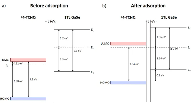
On the basis of the ARPES measurements, the band alignment of the F4-TCNQ/1TL GaSe heterostructure was also determined. Figure 4 illustrates the schematic energy level alignment diagrams before (panel a) and after (panel b) surface transfer doping. Based on literature,34 the HOMO-LUMO gap of F4-TCNQ, as obtained from
direct and inverse photoemission spectroscopy, is 3.1 eV. To obtain the ARPES spectrum of bulk F4-TCNQ, we have deposited a large thickness of F4-TCNQ molecules on top of the 1TL GaSe/graphene heterostructure. As shown in Figure S1a and S1b, the electronic structure of pure F4-TCNQ films at large thicknesses reveals that its HOMO peak is centered at 3.49 ± 0.01 eV and its leading edge is located at about 2.88 eV (in a flat band condition). Thus, the F4-TCNQ LUMO minimum is positioned at 0.22 eV above the Fermi level. As we established in our previous work on 1TL GaSe/graphene vdW systems,7 the probed electron quasiparticle band gap of 1TL GaSe,
extracted from scanning tunneling microscopy/scanning tunneling spectroscopy STM/STS, is 3.5 eV. Since the position of the VBM found by our ARPES study is 2.3 eV BE, the conduction band minimum of 1TL GaSe is localized at a BE Ec of 1.2 eV above the Fermi level. Once the molecule-1TL GaSe contact is formed (the Fermi
energies of the molecules and the substrate are referenced to the same energy level), a transfer and redistribution of charges at the F4-TCNQ/1TL GaSe interface essentially take place until the equilibrium is reached, thereby yielding a HOMO edge shift from 2.88 eV to 3.04 eV BE. Since the HOMO and LUMO edges of the molecule are lower than the valence and conduction band edges of GaSe, we obtain a type II band alignment for the F4-TCNQ/1TL GaSe heterostructure with the advantage of electron-hole pair separation (i.e., electrons are confined in F4-TCNQ, while holes are confined in GaSe). Consequently, these observations, revealing that the band alignment is of type II, are remarkable for future electronic and optoelectronic technological applications.
Overall, this indicates that the interlayer hybridization between F4-TCNQ and GaSe is not strong, leading only to a reduction in the preexisting negative doping of 1TL GaSe generated by graphene, without affecting the integrity of the electronic band structure of GaSe in the reciprocal space. One should note that in addition to these measurements, we have performed further experiments on 7TL GaSe, by evaporating the same amount of molecules on its surface. Figure S2a displays the measured band structure of F4-TCNQ/7 TL GaSe, taken at a photon energy of 60 eV along the GaSe ΓK-ΓK’ high symmetry direction. By comparing the ARPES map of Figure S2a with the one acquired in our previous work on pristine 7TL GaSe,16 we notice that, as in the case of
1TL GaSe, the 7TL GaSe electronic states are blurred upon molecular deposition. To precisely determine the position of the VBM of 7TL GaSe, we have integrated the photoelectron intensity image of Figure S2a in order to obtain the energy distribution curve near Γ in the binding energy range of -5 eV to 0.4 eV (Figure S2b). From Figure S2b, we conclude that the VBM of F4-TCNQ/7TL GaSe is located at -0.58 eV bellow the Fermi energy. Note that in the pristine sample, the 7TL GaSe VBM was located at the Γ point at a binding energy of about -0.73 eV with respect to the Fermi level. This designates that after the molecular adsorption, the overall electronic structure of multilayered GaSe has rigidly upshifted toward lower binding energies by an amount of 0.15 eV. This energy shift value is almost identical to the VBM shift observed for 1TL GaSe (0.16 eV). Consequently, the deposition of the same amount of molecules on single and multilayered GaSe induces the same effects, i.e., approximatively similar energy shifts in the electronic band structure regardless the number of layers. Thus, in both samples, the excess negative charge of GaSe has been reduced after F4-TCNQ adsorption. Conduction transport measurements to confirm the reduced n-type doping of the system will be of utmost interest, they nevertheless remain quite difficult to implement. The GaSe layer is deposited on graphene substrate and the latter will drive the transport properties. Top gate using electrolyte may be a possible alternative, but will likely affect the redox state of the F4-TCNQ molecule before changing the carrier density within the GaSe semiconductor. Additionally, the stability of GaSe remains limited to a few hours’ time scale in air, which even further raises the complexity of fabrication and transport measurements. This strategy to obtained a doped layer thanks to molecular gating, even though with less tunability than conventional gating though a gate, is easier to integrate at the device level since neither additional electrode, nor fabrication steps are required.
Conclusion:
In conclusion, we performed a combined XPS and ARPES study of the F4-TCNQ/1TL GaSe heterostructure. No signature of a relevant hybridization effect between the deposited molecules and the 1TL GaSe/graphene heterostructure underneath, modifying the electronic properties of the system, has been detected. On the other hand, a reduced n-type doping of the system, translated by an upward displacement of the 1TL GaSe electronic band structure toward the Fermi level, takes place—attributed to an electron transfer from single TL GaSe to the F4-TCNQ molecules. Therefore, F4-TCNQ molecules constitute effective doping agents to reduce the excess negative charge of MX materials such as GaSe and InSe. Such doping processes in 2D materials are of great importance for potential device applications.
Acknowledgements: We acknowledge the financial support by RhomboG (ANR-17-CE24-0030) grants. This work is supported by a public grant overseen by the French National Research Agency (ANR) as part of the “Investissements d’Avenir” program (Labex NanoSaclay, reference: ANR-10-LABX-0035).
Corresponding Authors: *E-mail: [email protected]
*E-mail: [email protected]
Competing financial interests: The authors declare no competing financial interests.
Figure Captions:
Figure 1: a) A sketch of the F4-TCNQ layer incorporated on top 1TL GaSe grown on bilayer graphene/SiC(0001) substrate. An interfacial electron transfer from 1TL GaSe to F4-TCNQ occurs at the interface, where F4-TCNQ is negatively charged and GaSe presents a reduced excess n-type doping. b) XPS survey spectra of pristine single layer GaSe and F4-TCNQ/1TL GaSe, acquired with an incident photon energy of 825 eV, showing the successful deposition of F4-TCNQ on top of GaSe.
Figure 2: a) Photoemission spectra of Ga 3d (panel a and b), N 1s (panel c) and F 1s (panel d) core levels, taken on both 1TL GaSe (black circles) and F4-TCNQ/1TL GaSe (red circles), and recorded at photon energies of 60 eV (Ga 3d) and 825 eV (N 1s and F 1s). The core level peak of Ga 3d shows a rigid shift of 0.16 eV towards lower binding energies upon F4-TCNQ adsorption; this downshift is highlighted by a blue dashed line. In addition, N 1s core level can be fitted by means of three components, assigned to N-1 and N0 species, and shake up processes.
Figure 3: a) Comparison of the ARPES images for pristine single TL GaSe (left panel) and the F4-TCNQ/1TL GaSe heterostructure (right panel), acquired with a photon energy of 60 eV along the GaSe ΓK- ΓK’ high symmetry direction. b) and c) Second derivative spectra and energy distribution curves obtained from the intensity maps of photoelectrons in Figure 3a, respectively. As noticed from the ARPES images and spectra, the overall electronic structure rigidly upshifts of about 0.16 eV towards the Femi energy, showed by a white dashed line and located at 0 eV. Blue lines are Gaussian fits to extract the center of the dispersionless features, which can be attributed to several frontier orbitals of F4-TCNQ and to F4-TCNQ/1TL GaSe interface; the center of these features is marked by arrows.
Figure 4: Schematic energy level diagrams before (panel a) and after (panel b) the incorporation of F4-TCNQ molecules on the surface of 1TL GaSe, obtained from the ARPES measurements. The band gap values of 1TL GaSe and F4-TCNQ have been extracted from literature.7,34
References:
1 K. S. Novoselov, A. K. Geim, S. V. Morozov, D. Jiang, Y. Zhang, S. V. Dubonos, I. V. Grigorieva, and A. A.
Firsov, Science (80-. ). 306, 666 (2004).
2 R. Lu, J. Liu, H. Luo, V. Chikan, and J. Z. Wu, Sci. Rep. 6, 19161 (2016).
3 H. Huang, P. Wang, Y. Gao, X. Wang, T. Lin, J. Wang, L. Liao, J. Sun, X. Meng, Z. Huang, X. Chen, and J.
Chu, Appl. Phys. Lett. 107, 143112 (2015).
4 P. A. Hu, L. Wang, M. Yoon, J. Zhang, W. Feng, X. Wang, Z. Wen, J. C. Idrobo, Y. Miyamoto, D. B.
Geohegan, and K. Xiao, Nano Lett. 13, 1649 (2013).
5 S. Lei, L. Ge, Z. Liu, S. Najmaei, G. Shi, G. You, J. Lou, R. Vajtai, and P. M. Ajayan, Nano Lett. 13, 2777
(2013).
6 X. Li, M.-W. Lin, A. A. Puretzky, J. C. Idrobo, C. Ma, M. Chi, M. Yoon, C. M. Rouleau, I. I. Kravchenko, D.
B. Geohegan, and K. Xiao, Sci. Rep. 4, 5497 (2014).
7 Z. Ben Aziza, D. Pierucci, H. Henck, M. G. Silly, C. David, M. Yoon, F. Sirotti, K. Xiao, M. Eddrief, J.-C.
Girard, and A. Ouerghi, Phys. Rev. B 96, 035407 (2017).
8 W. Kim, C. Li, F. A. Chaves, D. Jiménez, R. D. Rodriguez, J. Susoma, M. A. Fenner, H. Lipsanen, and J.
Riikonen, Adv. Mater. 28, 1845 (2016).
9 V. Capozzi and M. Montagna, Phys. Rev. B 40, 3182 (1989).
10 R. Le Toullec, M. Balkanski, J. M. Besson, and A. Kuhn, Phys. Lett. A 55, 245 (1975). 11 R. H. Bube and E. L. Lind, Phys. Rev. 115, 1159 (1959).
12 J. M. Auerhammer and E. R. Eliel, Opt. Lett. 21, 773 (1996).
13 N. B. Singh, D. R. Suhre, V. Balakrishna, M. Marable, and R. Meyer, Prog. Cryst. Growth Charact. Mater. 37,
47 (1998).
14 P. A. Hu, Z. Wen, L. Wang, P. Tan, and K. Xiao, ACS Nano 6, 5988 (2012).
15 F. Withers, O. Del Pozo-Zamudio, A. Mishchenko, A. P. Rooney, A. Gholinia, K. Watanabe, T. Taniguchi, S.
J. Haigh, A. K. Geim, A. I. Tartakovskii, and K. S. Novoselov, Nat. Mater. 14, 301 (2015).
16 Z. Ben Aziza, H. Henck, D. Pierucci, M. G. Silly, E. Lhuillier, G. Patriarche, F. Sirotti, M. Eddrief, and A.
17 X. Zhou, M. Pfeiffer, J. Blochwitz, A. Werner, A. Nollau, T. Fritz, and K. Leo, Appl. Phys. Lett. 78, 410
(2001).
18 B. Maennig, M. Pfeiffer, A. Nollau, X. Zhou, and K. Leo, Phys. Rev. B 64, 195208 (2001).
19 E. L. Hanson, J. Guo, N. Koch, J. Schwartz, and S. L. Bernasek, J. Am. Chem. Soc. 127, 10058 (2005). 20 W. Gao and A. Kahn, Appl. Phys. Lett. 79, 4040 (2001).
21 J. Blochwitz, M. Pfeiffer, T. Fritz, and K. Leo, Appl. Phys. Lett. 73, 729 (1998). 22 W. Gao and A. Kahn, J. Appl. Phys. 94, 359 (2003).
23 S. Kazaoui, Y. Guo, W. Zhu, Y. Kim, and N. Minami, Synth. Met. 135–136, 753 (2003).
24 T. Takenobu, T. Kanbara, N. Akima, T. Takahashi, M. Shiraishi, K. Tsukagoshi, H. Kataura, Y. Aoyagi, and
Y. Iwasa, Adv. Mater. 17, 2430 (2005).
25 Y. Nosho, Y. Ohno, S. Kishimoto, and T. Mizutani, Nanotechnology 18, 415202 (2007). 26 H. Pinto, R. Jones, J. P. Goss, and P. R. Briddon, J. Phys. Condens. Matter 21, 402001 (2009). 27 W. Chen, S. Chen, D. C. Qi, X. Y. Gao, and A. T. S. Wee, J. Am. Chem. Soc. 129, 10418 (2007).
28 C. Coletti, C. Riedl, D. S. Lee, B. Krauss, L. Patthey, K. von Klitzing, J. H. Smet, and U. Starke, Phys. Rev. B
81, 235401 (2010).
29 T. Cao, Z. Li, and S. G. Louie, Phys. Rev. Lett. 114, 236602 (2015).
30 L. T. Vinh, M. Eddrief, J. E. Mahan, A. Vantomme, J. H. Song, and M.-A. Nicolet, J. Appl. Phys. 81, 7289
(1997).
31 A. Koma, J. Cryst. Growth 201–202, 236 (1999).
32 Z. Ben Aziza, V. Zólyomi, H. Henck, D. Pierucci, M. G. Silly, J. Avila, S. J. Magorrian, J. Chaste, C. Chen,
M. Yoon, K. Xiao, F. Sirotti, M. C. Asensio, E. Lhuillier, M. Eddrief, V.I. V. I. Fal’Ko, and A. Ouerghi, Phys. Rev. B 98, 115405 (2018).
33 A. Amokrane, C. A. Sébenne, A. Cricenti, C. Ottaviani, F. Proix, and M. Eddrief, Appl. Surf. Sci. 123/124,
619 (1998).
34 W. Gao and A. Kahn, Org. Electron. 3, 53 (2002).
35 S. K. Wells, J. Giergiel, T. A. Land, J. M. Lindquist, and J. C. Hemminger, Surf. Sci. 257, 129 (1991). 36 J. M. Lindquist and J. C. Hemminger, J. Phys. Chem. 92, 1394 (1988).
37 D. Qi, W. Chen, X. Gao, L. Wang, S. Chen, P. L. Kian, and A. T. S. Wee, J. Am. Chem. Soc. 129, 8084
(2007).
38 N. Koch, S. Duhm, J. P. Rabe, A. Vollmer, and R. L. Johnson, Phys. Rev. Lett. 95, 237601 (2005). 39 S. Braun and W. R. Salaneck, Chem. Phys. Lett. 438, 259 (2007).
40 M. Knupfer, Surf. Sci. Rep. 42, 1 (2001).

![[PDF] Cours : Excel Budget Prévisionnel | Télécharger PDF](data:image/gif;base64,R0lGODlhAQABAIAAAP///wAAACH5BAEAAAAALAAAAAABAAEAAAICRAEAOw==)