RESEARCH OUTPUTS / RÉSULTATS DE RECHERCHE
Author(s) - Auteur(s) :
Publication date - Date de publication :
Permanent link - Permalien :
Rights / License - Licence de droit d’auteur :
Bibliothèque Universitaire Moretus Plantin
Institutional Repository - Research Portal
Dépôt Institutionnel - Portail de la Recherche
researchportal.unamur.be
University of Namur
Collective molecular switching in hybrid superlattices for light-modulated
two-dimensional electronics
Gobbi, Marco; Bonacchi, Sara; Lian, Jian X.; Vercouter, Alexandre; Bertolazzi, Simone;
Zyska, Björn; Timpel, Melanie; Tatti, Roberta; Olivier, Yoann; Hecht, Stefan; Nardi, Marco V.;
Beljonne, David; Orgiu, Emanuele; Samorì, Paolo
Published in:
Nature Communications
DOI:
10.1038/s41467-018-04932-z
Publication date:
2018
Document Version
Publisher's PDF, also known as Version of record
Link to publication
Citation for pulished version (HARVARD):
Gobbi, M, Bonacchi, S, Lian, JX, Vercouter, A, Bertolazzi, S, Zyska, B, Timpel, M, Tatti, R, Olivier, Y, Hecht, S,
Nardi, MV, Beljonne, D, Orgiu, E & Samorì, P 2018, 'Collective molecular switching in hybrid superlattices for
light-modulated two-dimensional electronics', Nature Communications, vol. 9, no. 1, 2661.
https://doi.org/10.1038/s41467-018-04932-z
General rights
Copyright and moral rights for the publications made accessible in the public portal are retained by the authors and/or other copyright owners and it is a condition of accessing publications that users recognise and abide by the legal requirements associated with these rights. • Users may download and print one copy of any publication from the public portal for the purpose of private study or research. • You may not further distribute the material or use it for any profit-making activity or commercial gain
• You may freely distribute the URL identifying the publication in the public portal ?
Take down policy
If you believe that this document breaches copyright please contact us providing details, and we will remove access to the work immediately and investigate your claim.
ARTICLE
Collective molecular switching in hybrid
superlattices for light-modulated two-dimensional
electronics
Marco Gobbi
1,6
, Sara Bonacchi
1,7
, Jian X. Lian
2
, Alexandre Vercouter
2
, Simone Bertolazzi
1
, Björn Zyska
3
,
Melanie Timpel
4
, Roberta Tatti
5
, Yoann Olivier
2
, Stefan Hecht
3
, Marco V. Nardi
4
, David Beljonne
2
,
Emanuele Orgiu
1,8
& Paolo Samorì
1
Molecular switches enable the fabrication of multifunctional devices in which an electrical
output can be modulated by external stimuli. The working mechanism of these devices
is often hard to prove, since the molecular switching events are only indirectly con
firmed
through electrical characterization, without real-space visualization. Here, we show how
photochromic molecules self-assembled on graphene and MoS
2generate atomically precise
superlattices in which a light-induced structural reorganization enables precise control over
local charge carrier density in high-performance devices. By combining different experimental
and theoretical approaches, we achieve exquisite control over events taking place from the
molecular level to the device scale. Unique device functionalities are demonstrated, including
the use of spatially confined light irradiation to define reversible lateral heterojunctions
between areas possessing different doping levels. Molecular assembly and light-induced
doping are analogous for graphene and MoS
2, demonstrating the generality of our approach
to optically manipulate the electrical output of multi-responsive hybrid devices.
DOI: 10.1038/s41467-018-04932-z
OPEN
1University of Strasbourg, CNRS, ISIS UMR 7006, 8 allée Gaspard Monge, F-67000 Strasbourg, France.2Laboratory for Chemistry of Novel Materials,
Center for Research in Molecular Electronics and Photonics, University of Mons, Place du Parc 20, 7000 Mons, Belgium.3Department of Chemistry and IRIS Adlershof, Humboldt-Universität zu Berlin, Brook-Taylor-Str. 2, 12489 Berlin, Germany.4Department of Industrial Engineering, University of Trento, Via Sommarive 9, 38123 Trento, Italy.5IMEM-CNR, Institute of Materials for Electronics and Magnetism, Trento unit, Via alla Cascata 56/C, Povo, 38123 Trento, Italy.6Present address: Centro de Fisica de Materiales (CSIC-UPV/EHU), Paseo Manuel de Lardizabal 5, E-20018 Donostia, San Sebastián, Spain. 7Present address: Department of Chemical Sciences, University of Padua, Via Francesco Marzolo 1, Padova, 35131, Italy.8Present address: Institut National
de la Recherche Scientifique (INRS), EMT Center, Boulevard Lionel-Boulet, Varennes, QC, J3X 1S2, 1650, Canada. Correspondence and requests for materials should be addressed to M.G. (email:[email protected]) or to P.S. (email:[email protected])
123456789
O
ne among the grand challenges of nanotechnology is the
precise manipulation of an electrical output in solid-state
devices through the control of molecular events occurring
at the nanoscale
1. By exploiting unique functions encoded in
specific molecular groups and modulated through external
sti-muli, multifunctional devices can be fabricated in which the
electrical conductance can be adjusted ad hoc, offering
sought-after solutions for sensing and opto-electronics
2.
For instance, photochromic molecules, which are capable of
switching between two (meta-) stable states when exposed to
specific wavelengths
3, enable the use of a photonic input to
modulate the electrical characteristics of solid-state devices
4–16.
Of particular interest is the possibility to exploit photochromic
molecules to modulate the conductance of (semi)conductive
materials, eventually leading to light-switchable macroscopic
devices
10–16. This approach was demonstrated for carbon
nanotubes
10,11, graphene
7,12,13, and polymers
14,15.
In all these studies, the isomerization was inferred on the basis
of the electrical characterization, without a direct, real-space
visualization of the (supra)molecular structural changes induced
by the switching events. As a consequence, the electrical effects
measured at the device level could not be rationalized in various
cases
12,13. On the contrary, real-space images of supramolecular
assemblies of photochromic molecules have been acquired
through scanning tunneling microscopy (STM)
17–21, but either
the photo-induced switching events could not be monitored
18,19or the specific experimental conditions hampered simple
trans-lation and integration in solid-state devices
17,20,21.
Two-dimensional materials
22(2DMs) represent an ideal
plat-form to study the interplay between molecular assembly on
surfaces and electrical transport in devices. On the exposed
sur-face of 2DMs, well-defined molecular groups can be arranged at
predetermined spatial locations with atomic precision by tailoring
of supramolecular architectures
23–25. Within these
organic/inor-ganic superlattices, macroscopic effects taking place at the device
scale can be understood on the basis of molecular functionality
and nanoscale arrangement
26–30, which can be directly accessed
by means of conventional surface-science techniques. Hitherto,
these highly controllable superlattices have not been exploited to
impart the switching properties of photochromic molecules to
2DMs.
Here we demonstrate optical control over the local charge
carrier density in high-performance devices by interfacing
supramolecular assemblies of photochromic molecules with
2DMs. In particular, we exploit the collective nature of
self-assembly to convert single-molecule isomerization events into a
spatially homogeneous switching action, which generates a
macroscopic electrical response in graphene and MoS
2. We
achieve exquisite control over such effects by combining
surface-science techniques and characterization of mesoscopic devices,
drawing a unified picture ranging from the scale of molecules all
the way to the device. Moreover, our superlattices enable the
demonstration of technologically relevant functions, such as the
reversible doping in graphene and MoS
2, and the use of spatially
confined light irradiation to pattern regions with well-defined
doping levels.
Results
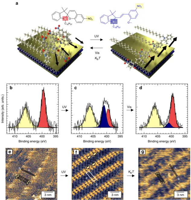
Photo-switchable hybrid superlattices. Our approach is
por-trayed in Fig.
1
a. The supramolecular assembly of photochromic
molecules at the surface of graphene and MoS
2single layers
generates an atomically precise superlattice in which a major
structural rearrangement is obtained by light-induced collective
isomerization. As a result, the rearrangement causes a reversible
shift in the 2DM work function, readable in devices as significant
doping, which is also fully reversible. For this study, we designed
and synthesized the spiropyran (SP) derivative bearing an
18-carbon long alkyl chain (Fig.
1
a and Supplementary Note
1
). SPs
are photochromic molecules
31that feature reversible
photo-chemical isomerization between a neutral closed-ring and a
zwitterionic open-ring isomer called merocyanine (MC),
char-acterized by a larger molecular dipole. In solution, the SP→MC
isomerization is triggered by irradiation with ultraviolet (UV)
light, while the MC→SP back isomerization is achieved either
thermally or via irradiation with visible light
31(Supplementary
Fig.
1
). The long alkyl chain promotes molecular self-assembly on
graphite and MoS
2, even at the monolayer limit
24–29,32–34. In
particular, the molecule–substrate and molecule–molecule
inter-play, dominated by van der Waals interactions, determines the
formation of highly ordered and closely packed lamellar
archi-tectures in which alkanes adsorb
flat on the surface
32,35,36and
which can be used as a template to decorate a given surface with
functional groups
26,27.
In order to study the photoswitch of the SP derivative down to
the monolayer limit, we performed X-ray photoelectron
spectro-scopy (XPS) and STM experiments at room temperature on dry
films on highly oriented pyrolytic graphite (HOPG) and MoS
2bulk crystals (see Methods section). Figure
1
b–g shows the results
obtained on HOPG, yet similar data were recorded on MoS
2(Supplementary Fig.
2
-
3
). XPS analysis of the binding energy of
the N 1s core level provides unambiguous identification of the
isomer on the surface, due to the very different hybridization of
the indoline N in SP and MC
18. In particular, the N 1s spectrum
of spin-coated SP
film (Fig.
1
b) has two contributions, with a
broad peak at binding energy E
b= 406.0 eV corresponding to
NO
2, and a sharper feature at E
b= 399.5 eV to the indoline N
atom. Following in situ UV irradiation, a new component
appeared at E
b= 401.0 eV (Fig.
1
c), which is a hallmark of the
MC isomer
18. Upon in situ irradiation with green light, an almost
complete recovery of the initial SP spectrum was observed
(Fig.
1
d). These data provide evidence that photo-isomerization
takes place on van der Waals substrates, in contrast with
analogous experiments on metallic surfaces
18,19.
The evolution of the molecular arrangement was monitored
with sub-nm resolution by STM imaging in air and at room
temperature on dry
films on HOPG and MoS
2(see Methods
section). In the SP monolayer, a lamellar structure was visualized,
in which different rows of alkanes lying
flat on the substrate are
separated by bright fuzzy regions, generating an atomically
precise superlattice (Fig.
1
e). The resulting packing gives rise to a
unit cell a
= 5.4 ± 0.2 nm, b = 0.45 ± 0.1 nm, and α = 83 ± 2°,
corresponding to an area A
= 2.5 ± 0.2 nm
2, with each unit cell
containing two SP molecules. The width of the lamellae,
amounting to 5.4 nm, is in good agreement with the sum of the
contour length of two SP molecules, indicating that the molecules
are assembling in a head-to-head fashion, as sketched in Fig.
1
e,
with the SP groups located in the bright regions separating
adjacent lamellae. The bright contrast can be ascribed to aromatic
SP head-groups, which owing to their non-planarity protrude
slightly from the surface, whereas the low resolution suggests that
the SP groups are not immobilized on the surface, and their
dynamics occur on a time scale faster than STM imaging.
Remarkably, the UV-light-triggered SP→MC isomerization
induces a profound reorganization of the assembly (Fig.
1
f). In
this case, the high-resolution images could be acquired
through-out the whole STM
field of view, indicating that fully immobilized
MC groups lie close to each other, while the alkyl chains form an
interdigitated lamellar structure. The packing of the MC phase
exhibits a unit cell a
= 4.1 ± 0.2 nm, b = 1.2 ± 0.1 nm, and α = 82
± 2°, which still contains two MC molecules but exhibits an area
A
= 4.7 ± 0.2 nm
2that is almost twice as large as compared to the
SP phase (Fig.
1
f). Such UV-light-induced major reorganization
of the molecular assembly was also observed in survey STM
images and by atomic force microscopy (AFM) at the
microscopic scale (Supplementary Fig.
4
). Owing to its metastable
nature, at room temperature the MC isomer thermally converts
back to the SP isomer in a few hours and thus gets back to
its initial nanoscale arrangement. The same UV-irradiated
film was imaged 48 h after irradiation, and an assembly similar
to the initial one was observed (Fig.
1
g), with practically identical
unit cell parameters (a
= 5.4 ± 0.2 nm, b = 0.4 ± 0.1 nm, and
α = 87 ± 2°). Such result is in line with spectroscopic
character-ization of thin
films monitoring the SP→MC isomerization and
subsequent thermal MC→SP recovery (Supplementary Fig.
1
).
Work function tuning through light irradiation. Molecular
mechanics/dynamics (MD) simulations combined with density
functional theory (DFT) calculations made it possible to fully
account for the molecular assembly as observed by STM imaging
(Supplementary Note
2
). In the SP case, the head-groups were
found to be mobile, i.e., conformationally
flexible, and hence
410 405 400 395
Binding energy (eV)
410 405 400 395
Binding energy (eV)
410 405 400 395
Binding energy (eV)
Intensity (arb. units.)
UV NO2 NO2 C18H37 C18H37 N N + O O –
a
Vis KBT 3 nm 3 nm 3 nme
f
g
UV KBT a b UV Visb
c
d
a b a bFig. 1 Photo-switchable molecular crystals in two dimensions. a Schematic representation of our approach. A spiropyran (SP) derivative forms ordered crystalline structures when deposited on different van der Waals substrates. In the cartoon, a MoS2single layer is depicted in which the yellow (blue) layer
represents the S-(Mo-) atomic plane. Photo-induced isomerization induces a structural rearrangement. The molecular dipoles (depicted as black arrows) are randomly oriented before irradiation, yet well aligned after UV irradiation, leading to a modification in the energetics of the van der Waals substrate. The chemical structure of the spiropyran (SP)–merocyanine (MC) derivative used in the study is also shown. b–d N 1s core-level spectra measured on the same spin-coated ultrathinfilm on highly oriented pyrolytic graphite (HOPG) (b) kept in dark, (c) after in situ UV irradiation, and (d) after subsequent irradiation with green light. Each spectrum is characterized by multiple peaksfitted by different components, corresponding to the different N hybridization. The colors of thefitting components recall those of the N atoms in (a). e–g Scanning tunneling microscopic imaging of SP assemblies on HOPG. Height images of the molecular assemblies obtained (e) after spin-coating the SP solution, (f) immediately after UV irradiation, and (g) 48 h after UV irradiation. A schematic sketch of the molecule is superimposed to the images to facilitate the visualization of the molecular ordering. Tunneling parameters:It= 20 pA (e, f, g), Vt= 1000 mV (e, g), 600 mV (f)
randomly oriented at any moment in time. A representative
snapshot of such time-evolving situation is shown in Fig.
2
a. On
the contrary, an ordered assembly was encountered for the
MC isomer, exhibiting an interdigitated structure with a unit cell
in good agreement with the experimentally observed one (Fig.
2
b
and Supplementary Fig.
5
). Importantly, the distinct assembly
featured by each isomer affects the overall energetics of the
underlying van der Waals layers differently. In particular,
the component of molecular electric dipoles perpendicular to the
surface (μ
z) exerts a polarization capable of shifting the surface
work function (WF) and therefore induces local doping
37. Based
on our simulations, a relatively low averaged vertical dipole was
estimated for SPs (μ
z= 0.23 D per molecule, Supplementary
Fig.
6
), since the randomly oriented dipoles of the NO
2groups
cancel out. In contrast, in the MC assembly the positively charged
side of the molecule is lifted up for every molecule, resulting in
a significant electrical dipole oriented perpendicular to the
substrate plane (μ
z= 1.7 D per molecule, Supplementary Fig.
5
).
The presence of positive vertical dipoles results in a WF reduction
(or n-type doping), the intensity of which is proportional to
the dipole magnitude.
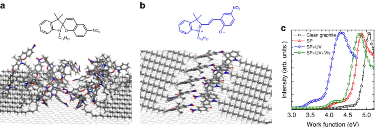
Experimentally, the evolution of the WF of HOPG and MoS
2was measured by UV photoemission spectroscopy, as a function of
the switching state of the molecular layer (see Methods section).
The presence of the SP
film introduces a WF decrease as
compared to the bare substrate, amounting to
ΔWF = −0.2 eV for
HOPG, which is indicative of n-type doping (Fig.
2
c).
Signifi-cantly, the UV-light-triggered SP→MC isomerization causes a
further, more pronounced WF decrease,
ΔWF = −0.7 eV for
HOPG, in good agreement with the theoretical
findings. Finally,
the green-light-triggered MC→SP switch is accompanied by an
almost complete recovery of the WF of the initial SP case (Fig.
2
c).
The same evolution in the WF shift was measured during the
photo-isomerization of the assembly on MoS
2(Supplementary
Fig.
6
).
Photo-switchable electrical characteristics in hybrid devices.
The WF shift translates into a change in the electrical
character-istics of devices based on single-layer 2DMs
29, offering
the possibility to convert the switching of the insulating
molecular crystal into a modulation in the electrical output
of high-performance devices. This effect was explored in
graphene and MoS
2devices with pristine mobility above 5000
and 30 cm
2V
−1s
−1, respectively (see Methods section). Figure
3
a
shows a scheme of the different steps involved in the experiment.
Initially, the transfer characteristics of devices based on clean
graphene and MoS
2were characterized. The measurement was
then repeated after spin-coating of the SP solution and UV
irradiation, which triggered SP→MC isomerization. Finally, the
initial 2DM/SP superlattice conductance was recovered by
irra-diating the whole
flake with green light. For graphene, a small
shift of the charge neutrality point was observed toward negative
values upon formation of the SP adlayer, corresponding to
minor n-type doping (Fig.
3
b). The SP→MC isomerization,
trig-gered by in situ UV irradiation, introduced a significantly stronger
n-type doping (induced electron density n
= 4.4 × 10
12cm
−2,
Fig.
3
b) and the initial graphene/SP characteristics could be
recovered by exposing the MoS
2surface with green light (Fig.
3
c).
At this point, a subsequent UV light irradiation could be
performed to prepare a second graphene/MC state characterized
by n-type doping, and the whole cycle could be repeated
(Sup-plementary Fig.
7
). Similarly to the case of graphene, for MoS
2the deposition of the ultrathin SP layer introduced a small
shift in the threshold voltage toward negative values (n-type
doping, Fig.
3
d). The UV-light-triggered SP→MC isomerization
caused a sizeable negative shift in the threshold voltage,
inducing an electron density n
= 4.6 × 10
12cm
−2(Fig.
3
d). The
electrical characteristics of MoS
2/SP could be recovered by
irradiating the entire
flake with green light (Fig.
3
e). Even for
MoS
2, a second n-doped MC/MoS
2state could be prepared by
UV light irradiation, and the whole cycle could be repeated
(Supplementary Fig.
7
). Thanks to the non-disruptive nature of
the non-covalent functionalization, the devices based on both
MoS
2and graphene preserved high electrical performances
after the formation of the SP and MC assemblies, retaining
mobilities above 25 and 4500 cm
2V
−1s
−1, respectively. We also
point out that the electrical characteristics of the SP/2DMs
superlattices could be recovered without green light exposure by
leaving the devices in dark for 24 h (Supplementary Fig.
8
) in
agreement with the thermal recovery observed in the optical
characterization (Supplementary Fig.
1
).
Numerous control experiments were performed to rule out
other possible mechanisms responsible for the electrical
changes induced by UV/visible light irradiation. In particular,
the UV irradiation was shown to induce a shift of the electrical
characteristics of 2DMs
38,39even without photochromic
mole-cules. In order to quantify this effect for our devices, we
performed UV irradiation on the pristine devices before the
formation of the SP layer. By using the same irradiation power
used in the experiments with the molecular superlattices, we
observed very minor effects in the case of both MoS
2and
graphene, as shown in Supplementary Fig.
8
.
3.0 N O C18H37 NO2 N + O – C18H37 NO2 3.5 4.0 4.5 5.0
Intensity (arb. units.)
Work function (eV)
Clean graphite SP SP+UV SP+UV+Vis
c
b
a
Fig. 2 Calculated assemblies and measured evolution of the substrate work function. a Representative snapshot of the calculated dynamic evolution of the spiropyran (SP) assembly.b Self-assembly of the merocyanine (MC) isomer. The positively charged region is lifted up. c Evolution of the work function of highly oriented pyrolytic graphite as a consequence of the isomerization of the photochromic assembly experimentally measured by ultraviolet photoemission spectroscopy. Such evolution of the work function can be fully explained on the basis of the (average) orientation of the vertical dipoles
ARTICLE
NATURE COMMUNICATIONS | DOI: 10.1038/s41467-018-04932-zTo further confirm that the strong n-type doping observed can
be fully ascribed to the presence of the MC assembly atop,
graphene and MoS
2devices were covered by a layer of MC,
obtained by irradiating SP in solution prior to deposition by
spin-coating. In this way, the devices were not irradiated with UV
light, and the effect of the MC layer could be separately
addressed. Figure
4
a, b show that the so-obtained MC layer
introduced significant n-type doping in graphene and MoS
2,
qualitatively and quantitatively similar to that observed upon
direct irradiation of the SP assembly. Interestingly, in the case of
graphene a dip in the electrical characteristics was observed at
approximately V
GS= 0 V after the formation of the MC layer. We
interpret such feature as originating from a graphene region
covered by SP rather than by MC isomers. Indeed, the MC→SP
back switch in solution takes place in a few seconds
(Supple-mentary Fig.
1
), and thus a significant fraction of SP molecules
are spin-coated on the substrate together with the MC. In
addition, we studied the nanoscale assembly obtained by directly
spin-coating MC molecules on HOPG, as shown in Fig.
4
c.
Notably, also the directly deposited MC assembly is analogous to
that obtained after UV irradiation of the dry SP
film, further
highlighting the direct correlation between nanoscale ordering
and doping effects.
Spatially con
fined modulation of charge carrier density. Our
system also allows the control over the local charge carrier
density, as shown in Fig.
5
for graphene. In this case, while
the UV light irradiates the whole area of the 2DM, the green
light is shone only on a spatially confined region of the flake
by using a focused laser (Fig.
5
a and Methods section). Similarly
to the case of Fig.
3
, significant n-type doping was introduced
by the SP→MC isomerization, triggered by in situ UV
irradiation over the whole graphene area (Fig.
5
b). Instead, the
spatially confined green light irradiation resulted in a double
feature in the electrical characteristics of the device (Fig.
5
c),
indicative of the presence of both SP and MC on the graphene
surface. Indeed, the region in the graphene/MC superlattice
exposed to the green laser fully recovered the almost undoped
graphene/SP state, while the unexposed molecular layer
main-tained MC character, inducing stronger n-type doping. This
experiment demonstrates our ability to create a dynamic
het-erojunction within the 2DM/photochromes superlattice. Such
laser-induced modulation of charge carrier density with
micro-metric resolution has a high technological potential, as it might
enable the realization of unconventional device architectures
in which a p-type transistor could be reversibly converted into
a rectifying p–n junction.
0 1 2 3 4 5 IDS ( µ A) IDS ( µ A) IDS ( µ A) IDS ( µ A) 2 SP 3 MC 4 SP 2 SP 3 MC 4 SP –30 –20 –10 0 10 20 30 0 1 2 3 4 Spiropyran deposition UV Vis 5 1 Clean graphene 2 SP 3 MC 1 Clean MoS2 2 SP 3 MC VGS (V) –30 –20 –10 0 10 20 30 VGS (V) –30 –20 –10 0 10 20 30 VGS (V) –30 –20 –10 0 10 20 30 VGS (V) 0 2 4 6 8 0 2 4 6 8 UV Vis UV Vis 1 2 3 3 2 4 1 2 3 4 2 3c
e
b
d
a
1 2 3 4Fig. 3 Electrical characteristics of devices based on photo-switchable superlattices. Transfer characteristics (IDS–VGS) of devices based on graphene and
MoS2superlattices.IDSis the drain current, andVGSis the gate potential.a Schematics of the experiment.IDS–VGScharacteristics are measured on: (1) A
2DM-based clean device; (2) after spin-coating of the spirofilm; (3) after irradiation with a UV light over the whole flake, which triggers the SP→MC isomerization; (4) after green light irradiation over the wholeflake, which triggers the MC→SP isomerization. Gold contacts are schematically drawn in yellow, the 2DM in dark gray; the substrate in blue; the SP layer in semi-transparent red; the MC layer in semi-transparent green.b Trace 1 (black): clean graphene, trace 2 (red): graphene covered by the SP layer, trace 3 (blue): graphene/MC after UV irradiation over the wholeflake. The arrow highlights the negative shift in the threshold voltage accompanying the SP→MC isomerization, indicative of n-type doping. c Trace 4 (green): recovered graphene/SP after green light irradiation of the whole graphene surface. Traces 2 and 3 are replotted for clarity (dashed).d Trace 1 (black): clean MoS2, trace 2 (red):
MoS2covered by the SP layer, trace 3 (blue): MoS2/MC after UV irradiation over the wholeflake. e Trace 4 (green): the pristine MoS2/SP trace can be
recovered upon irradiation of the whole surface with green light. Traces 2 and 3 are replotted for clarity. Details about the UV and green light irradiation are given in the Methods section; the transfer curves were measured applying a drain source voltageVDS= 10 mV for graphene (b, c) and VDS= 100 mV
1 SP 2 MC 3 SP+MC
c
b
UV –30 –20 –10 0 10 20 30 –30 –20 –10 0 10 20 30 0 1 2 3 4 5 0 1 2 3 4 5 1 SP 2 MC IDS ( µ A) IDS ( µ A) VGS (V) VGS (V) 2 3a
1 UV 2 1 Confined VisFig. 5 Spatially confined doping in photo-switchable superlattices. Transfer characteristics (IDS–VGS) of devices based on graphene and MoS2superlattices.
IDSis the drain current, andVGSis the gate potential.a Schematics of the experiment.IDS–VGScharacteristics are measured for: (1) The graphene device
covered by the SPfilm; (2) After UV light irradiation over the whole superlattice, which triggers the SP→MC isomerization; (3) After green light irradiation in a well-defined area of the active layer, which triggers the MC→SP isomerization in the irradiated area. Gold contacts are schematically drawn in yellow, graphene in dark gray; the substrate in blue; the SP layer in semi-transparent red; the MC layer in semi-transparent green.b Trace 1 (red): graphene covered by the SP layer, trace 2 (blue): graphene/MC after UV irradiation over the wholeflake. The arrow highlights the negative shift in the threshold voltage accompanying the SP→MC isomerization, indicative of n-type doping. c Trace 3 (green solid line): graphene/MC+SP, obtained by local irradiation with green light. Traces 1 and 2 are replotted. Details about the UV and green light irradiation are given in the Methods section; the transfer curves were measured applying a drain-source voltageVDS= 10 mV. Channel length L = 8.9 µm and width W = 1.0 µm
–30 –20 –10 0 10 20 30 10 20 30 40 50 IDS ( µ A) IDS ( µ A) VGS (V) –30 –20 –10 0 10 20 30 VGS (V) Clean graphene MC 0 4 8 12 16 20 24 Clean MoS2 MC
d
c
b
3 nma
Merocyanine deposition a bFig. 4 Effect of the direct deposition of the merocyanine isomer. a Schematics of the experiment. Transfer characteristics (IDS–VGS) are measured for clean
graphene and MoS2devices before and after the deposition of a merocyaninefilm. b IDS–VGSof a clean graphene device (in black) and of the same device
covered by a directly deposited merocyanine (MC) assembly (in blue).cIDS–VGSof a clean MoS2device (in black) and of the same device covered by a
directly deposited MC assembly (in blue). The directly deposited MC layer introduced significant n-type doping in both graphene and MoS2, qualitatively
and quantitatively similar to that observed upon irradiation of the spiropyran assembly on the devices. The transfer curves were measured applying a drain source voltageVDS= 10 mV for graphene and VDS= 1 V for MoS2. Channel lengthL = 4.6 µm and width W = 10.6 µm (graphene); L = 1.4 µm, W = 1.0 µm
(MoS2).d Scanning tunneling microscope height image of the assembly of a directly deposited MCfilm on highly oriented pyrolytic graphite. Measured
unit cell parameters:a = 3.9 ± 0.2 nm, b = 1.1 ± 0.1 nm, and α = 90 ± 2°, therefore leading to an area A = 4.2 ± 0.2 nm2. Inset: Calculated MC assembly on the basis of molecular dynamics simulations. Tunneling parameters: average tunneling currentIt= 20 pA, tip bias voltage Vt= 600 mV. In the three cases,
the SP→MC isomerization was obtained through irradiation of an SP solution with UV light immediately before spin coating
Discussion
In this work, we have demonstrated multi-responsive devices
relying on a collective switching action of photochromic
mole-cules self-assembled on the surface of 2DMs. By combining
dif-ferent experimental and theoretical approaches, we achieve an
ultra-high control over our system. An analogous control over
switching events and molecular assembly was previously
demonstrated in the so-called dynamic molecular crystals, i.e.,
self-assembled crystalline structures (typically three-dimensional)
in which macroscopic structural changes arise from collective
molecular events
40–42. However, the bulk dynamic molecular
crystals are typically bad electrical conductors and incompatible
with macroscopic device operation, since the chemical structure
of molecular switches is not designed for efficient charge
trans-port. In this respect, our approach enables the integration of a
functional supramolecular assembly, which represents the
quasi-two-dimensional (2D) limit of molecular dynamic crystals, in
high-performance devices to demonstrate switchable electric
outputs.
The highly controllable manipulation of the charge density
demonstrated in our superlattices presents several aspects of
technological relevance. Precise control of the local carrier density
(doping) is a key technology in semiconductor industry
43. Most
electronic
devices—including
diodes
and
metal-oxide-semiconductor
field-effect transistors—are based on the
possibi-lity to generate regions within a semiconductor with spatially
varying doping
43. In our superlattices, the doping effect is
tun-able, reversible, and cyclable. Moreover, we demonstrated lateral
heterojunctions between areas characterized by different doping
levels, defined by scanning a laser light over the target areas in the
superlattice. All together, these characteristics make our control
over the doping in 2DMs unique. Unconventional device
archi-tectures can be envisaged, such as diodes in which the p- and
n-regions can be re-defined and inverted, resulting in tunable and
reversible rectification.
Our approach, relying on molecular engineering of 2DMs, is of
general applicability as successfully demonstrated for both MoS
2and graphene. Therefore, the ultrathin photo-switchable
mole-cular crystals could be integrated as an additional quasi-2D layer
in vertical inorganic van der Waals heterostructures
44with the
purpose of providing a photo-responsivity with no analog in
2DMs. Our work offers a yet unexplored solution to
supramo-lecular electronics, in which atomic precision in mosupramo-lecular
self-assembly is tailored not to optimize charge transport but rather to
control it by imparting new properties to a high-performing
material, enabling the realization of multifunctional,
high-performance devices.
Methods
Synthesis and characterization of the SP derivative. Full details regarding the characterization and synthesis of the SP derivative are given in Supplementary Note1.
Optical characterization. Absorption spectra were recorded at room temperature (25 °C) with a JASCO V-670 spectrophotometer and all solutions were examined in quartz cells with 1 cm pathlength (HELLMA) with a concentration of 0.05 mg mL−1. The thin-film experiments were carried out in a nitrogen atmosphere.
X-ray and UV photoelectron spectroscopy. Surface XPS/UPS studies were per-formed at the BEAR endstation (BL8.1L) at the left exit of the 8.1 bending magnet of the ELETTRA synchrotron facility in Trieste (Italy). The data were collected using a hemispherical electron energy analyzer with an energy resolution of 150 meV in normal emission geometry. Photon energies of 505 and 640 eV were used for the N 1s and O 1s core levels, respectively. In this way, the kinetic energy of the emitted photoelectrons was kept at∼100 eV for each chemical species to probe similar sample depths with high surface sensitivity. For the determination of the work function, the secondary electron cutoff spectra were measured using a photon energy of 40 eV, with the sample biased at−20 V to clear the analyzer work
function. For the synchrotron measurements, the samples were irradiated in situ in ultra-high-vacuum using an opticalfiber positioned close to the sample surface available at the BEAR beamline. The UV light irradiation (λ = 375 nm) was per-formed with power density comparable with that used for the 2D assembly iso-merization described below. Instead, owing to the technical impossibility of focusing a green laser to a spot of a few micrometers at the beamline, the green light irradiation (λ = 532 nm) was carried out with significantly lower power (1 mW cm−2) than that used for inducing the isomerization of the 2D assembly described above. Full details regarding the X-ray photoemission electron micro-scopy (XPEEM) images of MoS2flakes used for device fabrication (see below) are
given in Supplementary Fig.9.
2D assembly formation and SP-to-MC isomerization. The 2D assemblies at the monolayer limit were obtained by spin-coating molecules from cyclohexane solutions (0.1 mg mL−1) onto either HOPG or MoS2bulk crystals for STM
experiments and onto single-layer MoS2and graphene devices. A mild annealing of
the samples (55 °C, 30 min) after spin-coating the SPfilm was performed to ensure the evaporation of cyclohexane. In order to trigger the SP→MC isomerization, the so-obtained assemblies were irradiated with an UV lamp (UV-6 L/M Herolab,λ = 365 nm, power density= 1.7 mW cm−2) for 45 min in a nitrogen-filled glovebox. MC-to-SP isomerization. The MC→SP isomerization was obtained by irradiation with a green laser focused to a size of 2 × 2μm2through a 50× objective in a confocal Renishaw InVia Raman microscope (λ = 532 nm, power P = 30 μW, exposure time t= 0.1 s). For flakes with size >2 μm, the laser was scanned on the flake surface irradiating a spot every 200 nm. The focused laser allowed us to perform a spatially confined irradiation of a relatively big graphene flake in a device with a channel length >8μm by scanning the laser light only over a limited region of theflake. The samples were kept in a nitrogen-filled Linkam environmental chamber during the green irradiation.
STM and AFM. STM measurements were carried out by using a Veeco Scanning Tunneling microscope (multimode Nanoscope III, Veeco) operating with a pie-zoelectric scanner, which allowed the mapping of a maximum area of 1 × 1 µm2. As substrates, we used HOPG and bulk MoS2(HQgraphene). The substrates were
glued onto a magnetic disk and an electric contact was made with conductive silver paint (Aldrich Chemicals). The STM tips were mechanically cut from a Pt/Ir wire (90/10, diameter 0.25 mm). The images were obtained in air at room temperature. The raw STM data were processed through the application of background flat-tening, and in Fig.1e–g in the main text the drift of the piezo was corrected using the underlying graphite lattice as a reference. The lattice of the underlying substrate was visualized by lowering the bias voltage Vtto 10 mV and keeping the same
average tunneling current It= 60 pA. Tip height and current were measured for all
STM images.
AFM characterization was carried out in a Multimode V (Veeco) microscope equipped with a Nanoscope V controller. Commercial silicon cantilevers with a nominal spring constant of 40 N m–1were used for morphological characterization in tapping mode.
Device fabrication and characterization. Back-gated devices based on scotch-tape exfoliated graphene and MoS2flakes were fabricated on SiO2(90 nm)/Si
substrates with a Microtech laser writer, equipped with a 405 nm laser standard photoresist (AZ1505, Microchemicals). A 35-nm-thick Aufilm (without adhesion layer) was thermally evaporated onto the patterned photoresist and lift-off was carried out in warm acetone (40 °C). After fabrication, the devices were immersed in warm n-methyl-2-pyrrolidone (40 °C) overnight and rinsed with acetone and isopropanol. The MoS2devices were annealed overnight in
ultra-high-vacuum at 140 °C. All devices were kept in a nitrogen-filled glove box in which they could be measured in a probe station connected to a Keithley 2636. After this procedure, the standard electrical characteristics of ideal graphene and MoS2
were measured. In particular, for the graphene device shown in Fig.3the charge neutrality point was found at VCNP= 0 V, with balanced hole–electron mobility
>5000 cm2V−1s−1. For MoS2, the device in Fig.3shows the typical characteristics
of MoS2transistors, with a mobilityμ = 32 cm2V−1s−1and intrinsic n-type
doping leading to a threshold voltage VT= −1 V. The reproducibility of the results
was verified by using five graphene and four MoS2devices. In both cases, the
results were in excellent qualitative and quantitative agreement with the data reported in Fig.3.
To ensure the quality of the device fabrication protocol, a representativeflake of a MoS2-based device was characterized in terms of surface chemical states and
relative elemental composition via XPEEM (see Supplementary Fig.9). The carrier mobility was determined using the formula:
μ ¼ dIDS dVGS L W t ε0εr ð1Þ where L and W are the 2DM channel length and width,ε0is the vacuum
permittivity, t is the thickness of gate oxide, andεris the relative dielectric
The isomerization-induced charge density was calculated as: Δn ¼ ε0εr
ΔV
et ð2Þ
where t is the thickness of gate oxide,ε0is the vacuum permittivity,εris the relative
dielectric permittivity of SiO2, and e is the elementary charge. For graphene,ΔV
was calculated as the difference in the position of the charge neutrality point before and after isomerization; for MoS2,ΔV was calculated as the difference in the
threshold voltage before and after isomerization.
MM and MD simulations. Full details regarding the MM/MD and DFT calcula-tions calculacalcula-tions are given in Supplementary Note2and Supplementary Fig.10.
Data availability. The data that support thefindings of this study are available from the corresponding authors on request.
Received: 17 November 2017 Accepted: 27 May 2018
References
1. Aradhya, S. V. & Venkataraman, L. Single-molecule junctions beyond electronic transport. Nat. Nanotechnol. 8, 399–410 (2013).
2. Chong‐an, D., Fengjiao, Z. & Daoben, Z. Multi‐functional integration of organicfield‐effect transistors (OFETs): advances and perspectives. Adv. Mater. 25, 313–330 (2012).
3. Feringa, B. L. & Browne, W. R. Molecular Switches (Wiley-VCH, Weinheim, 2011).
4. Whalley, A. C., Steigerwald, M. L., Guo, X. & Nuckolls, C. Reversible switching in molecular electronic devices. J. Am. Chem. Soc. 129, 12590–12591 (2007).
5. Mativetsky, J. M. et al. Azobenzenes as light-controlled molecular electronic switches in nanoscale metal-molecule-metal junctions. J. Am. Chem. Soc. 130, 9192–9193 (2008).
6. Kronemeijer, A. J. et al. Reversible conductance switching in molecular devices. Adv. Mater. 20, 1467–1473 (2008).
7. Margapoti, E. et al. Emergence of photoswitchable states in a graphene −azobenzene−Au platform. Nanoletters 14, 6823–6827 (2014). 8. Margapoti, E. et al. A 2D semiconductor-self-assembled monolayer
photoswitchable diode. Adv. Mater. 27, 1426–1431 (2015).
9. Jia, C. et al. Covalently bonded single-molecule junctions with stable and reversible photoswitched conductivity. Science 352, 1443–1446 (2016). 10. Guo, X., Huang, L., O’Brien, S., Kim, P. & Nuckolls, C. Directing and sensing
changes in molecular conformation on individual carbon nanotubefield effect transistors. J. Am. Chem. Soc. 127, 15045–15047 (2005).
11. Simmons, J. M. et al. Optically modulated conduction in chromophore-functionalized single-wall carbon nanotubes. Phys. Rev. Lett. 98, 86802 (2007). 12. Kim, M., Safron, N. S., Huang, C., Arnold, M. S. & Gopalan, P.
Light-driven reversible modulation of doping in graphene. Nano Lett. 12, 182–187 (2012).
13. Jang, A. et al. Reversibly light-modulated dirac point of graphene functionalized with spiropyran. ACS Nano 6(10), 9207–9213 (2012). 14. Orgiu, E. et al. Optically switchable transistor via energy-level phototuning in
a bicomponent organic semiconductor. Nat. Chem. 4, 675–679 (2012). 15. Orgiu, E. & Samorì, P. 25th anniversary article: organic electronics marries
photochromism: Generation of multifunctional interfaces, materials, and devices. Adv. Mater. 26, 1827–1844 (2014).
16. Suda, M., Kato, R. & Yamamoto, H. M. Light-induced superconductivity using a photoactive electric double layer. Science 347, 743–746 (2015).
17. Kumar, A. S. et al. Reversible photo-switching of single azobenzene molecules in controlled nanoscale environments. Nano Lett. 8, 1644–1648 (2008).
18. Piantek, M. et al. Reversing the thermal stability of a molecular switch on a gold surface: ring-opening reaction of nitrospiropyran. J. Am. Chem. Soc. 131, 12729–12735 (2009).
19. Schulze, G., Franke, K. J. & Pascual, J. I. Induction of a photostationary ring-opening— ring-closing state of spiropyran monolayers on the semimetallic Bi (110) surface. Phys. Rev. Lett. 109, 26102 (2012).
20. Dri, C., Peters, M. V., Schwarz, J., Hecht, S. & Grill, L. Spatial periodicity in molecular switching. Nat. Nanotechnol. 3, 649–653 (2008).
21. Bonacchi, S. et al. Surface-induced selection during in situ photoswitching at the solid/liquid interface. Angew. Chem. Int. Ed. 54, 4865–4869 (2015). 22. Fiori, G. et al. Electronics based on two-dimensional materials. Nat.
Nanotechnol. 9, 768–779 (2014).
23. Palma, C.-A. & Samorì, P. Blueprinting macromolecular electronics. Nat. Chem. 3, 431–436 (2011).
24. Wang, Q. H. & Hersam, M. C. Room-temperature molecular-resolution characterization of self-assembled organic monolayers on epitaxial graphene. Nat. Chem. 1, 206–211 (2009).
25. Macleod, J. M. & Rosei, F. Molecular self-assembly on graphene. Small 10, 1038–1049 (2014).
26. Mali, K. S., Greenwood, J., Adisoejoso, J., Phillipson, R. & De Feyter, S. Nanostructuring graphene for controlled and reproducible functionalization. Nanoscale 7, 1566–1585 (2015).
27. Phillipson, R. et al. Tunable doping of graphene by using physisorbed self-assembled networks. Nanoscale 8, 20017–20026 (2016).
28. Yu, Y. J. et al. Epitaxially self-assembled alkane layers for graphene electronics. Adv. Mater. 29, 1603925 (2017).
29. Gobbi, M. et al. Periodic potentials in hybrid van der Waals heterostructures formed by supramolecular lattices on graphene. Nat. Commun. 8, 14767 (2017).
30. Gobbi, M., Orgiu, E. & Samorì, P. When 2D materials meet molecules: opportunities and challenges of hybrid organic/inorganic van der Waals heterostructures. Adv. Mater. 30, 1706103 (2018).
31. Klajn, R. Spiropyran-based dynamic materials. Chem. Soc. Rev. 43, 148–184 (2014).
32. De Feyter, S. & De Schryver, F. C. Two-dimensional supramolecular self-assembly probed by scanning tunneling microscopy. Chem. Soc. Rev. 32, 139–150 (2003).
33. Lockhart De La Rosa, C. J. et al. Molecular doping of MoS2 transistors by self-assembled oleylamine networks. Appl. Phys. Lett. 109, 253112 (2016). 34. Wang, J. et al. Probing the crystallographic orientation of two-dimensional
atomic crystals with supramolecular self-assembly. Nat. Commun. 8, 377 (2017).
35. Rabe, J. & Buchholz, S. Commensurability and mobility in two-dimensional molecular patterns on graphite. Science 253, 424–427 (1991).
36. Shuxia, Y., Chen, W., Xiaohui, Q., Bo, X. & Chunli, B. Theoretical study of the effects of intermolecular interactions in self‐assembled long‐chain alkanes adsorbed on graphite surface. Surf. Interface Anal. 32, 248–252 (2001). 37. Christodoulou, C. et al. Tuning the work function of graphene-on-quartz
with a high weight molecular acceptor. J. Phys. Chem. C 118, 4784–4790 (2014).
38. Ju, L. et al. Photoinduced doping in heterostructures of graphene and boron nitride. Nat. Nanotechnol. 9, 348–352 (2014).
39. Singh, A. K. et al. Ultraviolet-light-induced reversible and stable carrier modulation in MoS2field-effect transistors. Adv. Funct. Mater. 24, 7125–7132 (2014).
40. Kobatake, S., Takami, S., Muto, H., Ishikawa, T. & Irie, M. Rapid and reversible shape changes of molecular crystals on photoirradiation. Nature 446, 778–781 (2007).
41. Koshima, H., Ojima, N. & Uchimoto, H. Mechanical motion of azobenzene crystals upon photoirradiation. J. Am. Chem. Soc. 131, 6890–6891 (2009). 42. Sato, O. Dynamic molecular crystals with switchable physical properties. Nat.
Chem. 8, 644–656 (2016).
43. Sze, S. M. & Ng, K. K. Physics of Semiconductor Devices (Wiley-VCH, Weinheim, 2007).
44. Novoselov, K. S., Mishchenko, A., Carvalho, A. & Castro Neto, A. H. 2D materials and van der Waals heterostructures. Science 353, aac9439 (2016).
Acknowledgements
We acknowledge funding from the European Commission through the Graphene Flagship (GA-785219), the Marie Sklodowska-Curie projects ITN project iSwitch (GA-642196) and IEF GALACTIC (PIEF-GA-2014-628563), and SUPER2D (GA-748971), the M-ERA.NET project MODIGLIANI, the Agence Nationale de la Recherche through the Labex projects CSC (ANR-10-LABX-0026 CSC) and NIE (ANR-11-LABX-0058 NIE) within the Investissement d’Avenir program (ANR-10-120 IDEX-0002-02), and the International Center for Frontier Research in Chemistry (icFRC) as well as the German Research Foundation (via SFB 765 and SFB 951). D.B. is a FNRS research director. M.V.N. and M.T. gratefully acknowledge the support by the CARITRO Foundation, (project MILA) Trento (Italy). Professor L. Pasquali, Dr. A. Giglia, and Dr. K. Koshmak are gratefully acknowledged for the help and stimulating discussions concerning the XPS and UPS measurements performed at the BEAR beamline at ELETTRA (proposal no. 20160339). Dr. L. Gregoratti, Dr. M. Amati, and Dr. H. Sezen are gratefully acknowledged for the help during the XPEEM sessions at ESCA microscopy beamline at ELETTRA (proposal no. 20160330).
Author contributions
M.G., S.Bo., E.O., and P.S. conceived the experiment. B.Z. and S.H. designed and syn-thesized the spiropyran derivative. M.G. performed the STM study and carried out the device fabrication and characterization with the aid of S.Be. S.Bo. performed the optical characterization of the molecules. M.T., R.T., and M.V.N. performed the XPS and UPS
experiments. J.X.L., Y.O., and D.B. performed the MD/DFT calculations. M.G. and P.S. co-wrote the paper. All authors discussed the results and contributed to the inter-pretation of data as well as to editing the manuscript.
Additional information
Supplementary Informationaccompanies this paper at https://doi.org/10.1038/s41467-018-04932-z.
Competing interests:The authors declare no competing interests.
Reprints and permissioninformation is available online athttp://npg.nature.com/ reprintsandpermissions/
Publisher's note:Springer Nature remains neutral with regard to jurisdictional claims in published maps and institutional affiliations.
Open Access This article is licensed under a Creative Commons Attribution 4.0 International License, which permits use, sharing, adaptation, distribution and reproduction in any medium or format, as long as you give appropriate credit to the original author(s) and the source, provide a link to the Creative Commons license, and indicate if changes were made. The images or other third party material in this article are included in the article’s Creative Commons license, unless indicated otherwise in a credit line to the material. If material is not included in the article’s Creative Commons license and your intended use is not permitted by statutory regulation or exceeds the permitted use, you will need to obtain permission directly from the copyright holder. To view a copy of this license, visithttp://creativecommons.org/ licenses/by/4.0/.