HAL Id: tel-01656305
https://hal-centralesupelec.archives-ouvertes.fr/tel-01656305
Submitted on 27 Feb 2018
HAL is a multi-disciplinary open access archive for the deposit and dissemination of sci-entific research documents, whether they are pub-lished or not. The documents may come from teaching and research institutions in France or abroad, or from public or private research centers.
L’archive ouverte pluridisciplinaire HAL, est destinée au dépôt et à la diffusion de documents scientifiques de niveau recherche, publiés ou non, émanant des établissements d’enseignement et de recherche français ou étrangers, des laboratoires publics ou privés.
harvesting devices: Modulation of the electronic
properties of graphene
Mohamed Boutchich
To cite this version:
Mohamed Boutchich. Bidimensional materials for low power and energy harvesting devices: Modu-lation of the electronic properties of graphene. Engineering Sciences [physics]. Université Pierre et Marie Curie (Paris 6), 2016. �tel-01656305�
A
CCREDITATION TO SUPERVISE RESEARCH
(H
ABILITATION À
D
IRIGER DES
R
ECHERCHES
)
OF
THE
U
NIVERSITY
P
IERRE AND
M
ARIE
C
URIE
(UPMC)
By
Mohamed Boutchich
Associate Professor in Electrical Engineering at UPMC ( CNU n°63)
Bidimensional materials for low power and energy harvesting
devices: Modulation of the electronic properties of graphene
Presented at Paris, June 1st 2016 :
Members of the Jury :
M. DELEONIBUS Simon, Director of Research CEA– LETI, Grenoble, Reviewer M. HAPPY Henri, Professor, IEMN–Lille 1, Reviewer
M. DANNEAU Romain, Senior scientist, KIT–Karlsruhe, Reviewer M. ODA Shunri, Professor – Tokyo Institute of Technology – Examiner M. MARANGOLO Massimiliano, Professor, INSP–UPMC, Examiner
M. ROCA i CABARROCAS Pere, Director of Research CNRS– LPICM, Ecole Polytechnique, Examiner M. KLEIDER Jean-Paul, Director of Research CNRS – GeePs, Examiner
Abstract
Since my appointment at the University Pierre ad Marie Curie (UPMC) in the Group of Electri-cal Engineering of Paris (GeePs) PHEMADIC division, my research interests focused on hete-rojunctions for nanoelectroniques and photo detection devices. Notably, I was interested in the integration of 2D materials that present a great potential for these topics. However, my first studies considered epitaxial diamond based power and UV detector heterojunctions. This work was a col-laboration with (LPICM-Ecole Polytechnique) and the National Institute for Material Science (Na-tional Institute for Material Science-Japan) that yielded a high on/off ratio device. Nevertheless, the difficulty to achieve pn junction on diamond hindered further development and I shifted my interest towards the modulation of the electronic properties of graphene keeping in mind the afo-rementioned applications. This new direction was possible thanks to strong national (Dr P. Roca i Cabarrocas du Laboratoire de Physique des Interfaces, Dr A. Ouerghi and Dr A. Madouri from Laboratoire de Photonique et Nanostructures - CNRS) and international partnerships (Pr S. Oda - Tokyo Institute of Technology, Pr Y Hee Lee - Sungkyunkwan University, Pr C.S Lai - Chang Gung University and Dr S. Kanjanachuchai - Chulalongkorn University) within the framework of the Labex NanoSaclay (post doc: F.Gunes (2012-2014) and Phd student H.Arezki (2012-2016)) and the ICT-ASIA programme (PhD K-I Ho (2013-2016)). In that context, we studied several he-terostructures such as e.g. silicon nanocrystals/graphene, fluorographene/graphene and memories, h-BN/graphene for field effect devices and transparent electrodes. Moreover, in collaboration with Dr K.Fukumoto and Pr S.Koshihara at Tokyo Institute technology, we have investigated the ul-tra fast carrier dynamics in CVD graphene superlattices by fs-PEEM (femtosecond-Photomession Electron Microscopy). We have been able to map the carrier lifetime accross a sample and we are trying to correlate the observation to the twist angle of the superlattices. In addition, I extended this collaboration to synchrotron Soleil in an attempt to observe the band structure of these superlatti-ces. Another field of research concerned the study of photovoltaic heterojunctions by modulated photo-luminescence technique (PhD student Ming Xu 2013-2016). Within the framework of ANR (SMASH 𝐼𝐵𝐶2) and European project (HERCULES) we have investigated and benchmarked va-rious passivation by measuring the carrier lifetime (ms for crystalline silicon as opposed to ps for graphene). In addition, we have extended the range of data available to the community for the radiative recombination coefficient B down to 20 K. This manuscript is structured around three different sections. The first section presents a detailled resume including my bibliography. In the second section, I will present a summary of my research activity. For the sake of clarity, I will only present my work since my appointment at the University Pierre and Marie Curie (UPMC)
as an Associate Professor in Electrical Engineering. Nevertheless, links to my previous research notably my work as a Senior Scientist at NXP-TSMC research centre (formely Philips Research Europe) will appear in the various sections. This second section througout the thesis I directed or co-directed will include my activity on (i)diamond and silicon based heterojunctions as well as (ii) bidimensional (2D) materials such as graphene. This latest was my main research topic for the last five years. The last section, will consider my propspective research for the coming 5 years dedicated to the low power applications of advanced materials. In this part, I will consider the exploitation of 2D layered materials for two domains : nanoelectronic memory devices based on a patent i recently filed and the integration of topological insulators (TI) in thermoelectric generators (TEG). I was acquainted to both domains since my PhD and I believe the remarkable properties of 2D materials may be of interest for the data retention and power consumption in non volatile memories on one hand but also improve the figure of merit in order to demonstrate thermoelectric generators using topological insulators.
Résumé en français
Depuis mon intégration à l’Université Pierre et Marie Curie (UPMC) au Laboratoire de Génie Electronique et Electrique de Paris (GeePs) pole PHEMADIC, je me suis intéressé aux hétéro-jonctions à base de semi-conducteurs pour les applications nanoélectroniques et de photo détection notamment l’intégration des cristaux bidimensionnels, qui présentent depuis l’avènement du grap-hene un fort potentiel applicatif. Mes premiers travaux au sein du pôle PHEMADIC ont porté sur le diamant épitaxié, matériau grand gap qui présente des propriétés remarquables pour la photo dé-tection UV et l’électronique de puissance. Dans ce contexte, en collaboration avec le Laboratoire de Physique des Interfaces et Couches Minces (LPICM-Ecole Polytechnique) et le National Insti-tute for Material Science (NIMS-Japon) nous avons développé une hétérojonction diamant (type p 500 nm)/a-Si:H (10 nm) à fort facteur de redressement. Néanmoins, la difficulté à produire du diamant de type N a ralenti le développement d’autres hétérojonctions. Dès lors, j’ai décidé de concentrer mes efforts sur le graphene cru sur des surfaces technologiquement viables. Mon axe de recherche s’articule autour de la caractérisation et la modulation des propriétés électroniques de ces matériaux 2D, j’ai étudié essentiellement deux types de graphene produit par mes parte-naires nationaux et internationaux. Dans ce cadre, et avec le soutien du labex NanoSaclay, j’ai pu mettre en place une plateforme GraPhIC (Graphene Growth Interface and Characterization) nous avons développé des instrumentations et des structures de test que nous avons caractérisé au sein du consortium (post doc: F.Gunes (2012-2014) et doctorant H.Arezki (2012-2016). Ces travaux ont permis d’acquérir une expertise dans des techniques spectroscopiques photo électroniques et Raman d’une part mais aussi de développer des composants nanoélectroniques tels que des tran-sistors tout graphene, des hétérostructures pour des applications photovoltaïques et mémoires. Ces travaux sont le fruit de collaborations fortes nationales (Dr P. Roca i Cabaroccas du Laboratoire de Physique des Interfaces, Dr A. Ouerghi et Dr A. Madouri du Laboratoire de Photonique et Na-nostructures - CNRS) et internationales (Pr S. Oda de Tokyo Institute of Technology, Pr Y Hee Lee de Sungkyunkwan University, Pr C.S Lai de Chang Gung University et Dr S. Kanjanachuchai de Chulalongkorn University) que j’ai pu établir via des invitations (Japon/Taiwan) et le projet 2D Nanotech (STIC-ASIE 2013-2015). Dans le cadre de ce projet, nous avons étudié différentes interfaces e.g. graphene/nanocrystaux (Pr S. Oda), graphene/fluorographene (Pr C.S Lai - docto-rant Kuan-I Ho 2013-2016). Mes travaux avec le Japon (Dr K.Fukumoto et Pr S.Koshihara) ont notamment porté sur la mesure de la dynamique ultra rapide des électrons dans des superstruc-tures en graphene par fs-PEEM (femtosecond-Photomession Electron Microscopy) développé au Tokyo Institute of Technology que je visite chaque année depuis 2012. Nous avons ainsi pu établir
une distribution spatiale de la dynamique des porteurs avec une technique originale et tentons de corréler les différentes dynamiques à l’angle de rotation entre chaque couche de graphene. Par ailleurs, mes travaux se sont étendus dans le cadre d’une collaboration avec le synchrotron Soleil pour la mesure des structures de bandes sur les superstructures en graphene CVD. Un second axe de recherche concerne l’étude des hétérojonctions photovoltaïques par des techniques de photo-luminescence notamment la photophoto-luminescence modulée. Nous avons développé des techniques de luminescence pour la mesure des propriétés à l’échelle micro/nanométrique et en fonction de la température (doctorant Ming Xu 2013-2016). Nous avons étudié différents type de passivati-ons dans le cadre de projet ANR (SMASH 𝐼𝐵𝐶2) et européen (HERCULES) pour déterminer le temps de vie des porteurs majoritaires (ms pour le silicium à opposer au ps pour le graphene) pour différents types d’hétérojonctions.
Ce manuscrit est constitué de trois parties : la première partie présente mon curriculum vitæ détaillé dans lequel j’y ai inclus ma bibliographie. Dans la seconde partie, je présente un ré-sumé de mes travaux de recherche. Dans un soucis de cohérence et clarté, je n’ai inclus que mes travaux depuis ma prise de fonction en tant que maitre de conférences à l’UPMC (2009). Néanmoins, des références à mes travaux antérieurs notamment en tant que scientifique au sein de la division recherche de NXP-TSMC Research Centre (IMEC - Leuven ex Philips Research Europe) apparaitront dans les différentes parties. Cette section au travers de mes encadrements et co-encadrements de thèse effectués durant la période 2009-2016 porte sur les travaux suivants : (i) heterojonctions à base de diamant et de silicium (ii) ingénierie des propriétés électroniques du graphene. Ce dernier point a constitué mon activité principale ces cinq dernières années. Enfin, dans la dernière partie, je propose deux axes de recherches pour les cinq prochaines années qui s’articulent sur l’étude des matériaux 2D (isolants topologiques inclus) et leur potentiel pour les applications électroniques basses puissances notamment les mémoires non volatiles et la conver-sion thermoélectrique. J’ai été amené à travailler sur ces deux sujets depuis mon doctorat et il m’apparait pertinent d’investiguer l’apport de la nanostructuration des matériaux 2D et de leurs propriétés électroniques remarquables sur la performance des mémoires à piégeage de charge en terme de réduction des puissance d’injection et de rétention des électrons d’une part et d’autre part démontrer une augmentation du facteur de mérite thermoélectrique en intégrant des isolants topologiques sur un concept de thermogénérateur que j’avais déja démontré en technologie mi-crosystème.
Table of contents
Abstract i
Résumé en français iii
1 Research activity 2009-2016 1
1.1 Foreword . . . 1
1.2 Diamond based heterojunctions . . . 2
1.3 Silicon based heterojunctions and interfaces . . . 5
1.3.1 Modulated photoluminescence and carrier lifetume measurement . . . . 5
1.3.2 Observation of the Excitation transfer in stacked quantum dot chains by micro PL - Collaboration with Chulalongkorn Unviversity - Thailand . . 8
1.4 Modulation of the electronic properties of graphene . . . 9
1.4.1 In situ nitrogen doping . . . . 10
1.4.2 Ex situ doping by nitric acid . . . . 13
1.4.3 CVD graphene/a-Si:H heterostructure . . . 15
1.5 Graphene/fluorographene heterostructures . . . 19
1.6 International collaborative research . . . 22
1.6.1 Toyohashi Tech - Japan - Graphene oxide . . . 22
1.6.2 Characterization of CVD graphene superlattices . . . 22
1.6.3 Synchrotron Soleil collaborative research - nanoARPES . . . 25
1.6.4 Tokyo Institute of Technology - Japan - Spatio-temporal observation of photogenerated electron dynamics in graphene superlattices . . . 25
1.6.5 Chang Gung University - Taiwan . . . 27
1.6.5.1 Graphene nanodiscs nonvolatile memory . . . 27
1.6.5.2 Multilayer graphene nanoribbons . . . 29
2 Prospective research topics 31 2.1 Foreword . . . 31
2.2 2D heterostructures for nonvolatile memory . . . 31
2.2.1 Revisiting the band gap engineered charge trapping memory concept . . . 31
2.2.2 What can we expect from 2D materials? . . . 33
2.3 Thermoelectric generator (TEG) . . . 40
2.3.1 Physical basis of low dimensional materials-based energy efficient devices 40
2.3.2 Thermoelectric generator . . . 44
2.4 Conclusions and Perspectives . . . 47
References 49
Chapter 1
Research activity 2009-2016
1.1
Foreword
My research started in 1999 during my PhD at the Institut d’Electronique de Microélectronique & de Nanotechnologies (IEMN-Lille, France) from 1999 to 20021. I designed, fabricated and characterized infrared sensors based on thermoelectric micro radiometer in MEMS technology. particularly, I developed a highly sensitive thermopile based on the doping of polysilicon ther-moelements2. This research led to the development of a new planar device using a suspended thermopile designed to prevent the encapsulation under atmosphere3.
Following my PhD, I joined The University of Cambridge Engineering Department (CUED) and the Centre for Advanced Photonics and Electronics (CAPE) as a research associate (06/2003-07/2006) in the Electronic Devices & Materials Group head by Pr W.I.Milne and under the su-pervision of Dr D.F Moore within the framework of an EPSRC funded project entitled APOEM (250k£) : Active Packaging for Optoelectronic and Electronic Microsystems. In this context, I utilized the experience acquired during my PhD to developed micromechanical structures for the alignment of photonics devices as well as characterization set up. Notably, I implemented a force measurement set up to measure mN forces delivered by thermomechanical microactuators4. In this framework, I’ve been involved in national and international collaborations with Tokyo University, Imperial College London, EPFL Lausanne as well as the company Micro Circuit Engineering that was interested in such MEMS devices for its products5–7. Moreover, I participated to the launch of Owlstonenanotech Ltd a spin off of CUED for which I prototyped as a consultant (06/2004 -07/2006) a field asymetric microspectrometer∗.
In 2006, I joined Philips Research (acquired by NXP and TSMC in 2008) Europe and became a senior scientist at NXP-TSMC Research Centre located at IMEC (Leuven, Belgium) & The High Tech Campus (Eindhoven, The Netherlands). I participated in different work packages in the NEMeSyS European Project (4M€)8developing future non-volatile memories for 45nm and beyond integrating advanced tunnel barriers such as charge trapping devices9. I was in charge of the technology and the characterization of advanced memory devices using high-k materials and metal gate. This work led to the demonstration of advanced charge trapping concepts based on the
integration of high-k and metal gate for 45 nm and beyond. This work was partly within the In-dustrial affiliated program within IMEC with various semiconductor research groups. I authored several technical notes on the topic10,11–13. I participated to the demonstration of a new program-ming mechansim entitled PAHHI (Punch Through Assisted Hot Holes Injection) to programme and erase thick tunnel oxide flash devices14. I filed four patents including a thermoelectric sensor using the CMOS integration technology to create a temperature gradient between two thermoele-ments15.
In September 2009, I was appointed as an Associate Professor in Electrical Engineering at Pierre and Marie Curie University (UPMC), Paris. I started my research on diamond based deviced and progresively shifted to graphene and photovoltaic heterostructures. I coordinated the pro-ject GraPhIC (Graphene growth Interfaces and Characterization) funded by Labex NanoSaclay in which we developed a characterization platform for graphene based devices as well as synthesis using CVD (post doctoral research associate Dr F. Gunes). From September to December 2012, I was an invited Associate Professor at the Quantum Nanoelectronic Research Centre (QNERC) at Tokyo Institute of Technology/Japan in Professor S.Oda’s lab. I closely work with Pr S. Kos-hihara and Dr K.Fukumoto whom i visit every year to investigate the lifetime in CVD graphene superlattices using their fs-PEEM technique. Since March 2013, I head the ICT-ASIA funded (2D Nanotech) research exchange programme in collaboration with Tokyo Institute of Techno-logy (Japan), SDRL (Chulalongkorn University-Thailand) and Semiconductors lab (Chang Gung University-Taiwan). I am also the French coordinator for an International nanoscience master de-gree (XNEM 2014-2017) funded by the EU-TEMPUS programme for the Middle East and North Africa region∗. I coordinate the semiconductors physics course and we will welcome 3 students at UPMC to carry out their master’s thesis.
1.2
Diamond based heterojunctions
My integration at GeePs lab (formely LGEP lab) started with the study of diamond based hete-rostructures. This work was a collaborative research between GeePs, the Physics of Interfaces and Thin film lab LPICM and the National Institute for Materials Science (NIMS - Japan). Despite the tremendous challenges to overcome for its synthesis and doping, diamond remains an attractive wide band gap semiconductor (5.5 eV) for a range of electronic devices especially those requiring high power and operating in harsh environment (temperature, radiations)16. Amongst the con-cepts that raised a lot of interest are Schottky-barrier diodes (SBD), Schottky-barrier Photodiode (SPD) as well as pn and p–i–n junction (PND) with (N)-doped diamond17–19. The development of reliable bipolar devices is a key technological building block for the design and fabrication of electronic devices. For that purpose, it is necessary to obtain device-grade quality for the n as well as the p- type diamond. Although various groups have devoted a lot of efforts to incorporate donor atoms such as (P)–Phosphorus or (As) –Arsenic into semiconductor diamond, the resisti-vity as well as junction characteristics such as built-in voltage and rectification ratio remain too
1.2 Diamond based heterojunctions 3
poor to envision competitive device. In addition, increasing the donor concentration beyond a certain level has proven to be detrimental to the diamond integrity. The aforementioned techno-logical issues to fabricate bipolar devices on diamond homojunctions have raised interest into the study of heterojunction with semiconductor materials such as aluminum nitride (AlN) or zinc ox-ide (ZnO)20,21. Such a structure combines the properties of both semiconductors and may lead to outstanding performance in terms of rectification ratio. Note that if these heterostructures are fabricated with transparent electrodes, pn and/or p–i–n diamond based heterojunctions find ap-plications in photo detection as well as light emitting diodes22. In our work we have integrated amorphous silicon (a-Si:H). 500 nm thick diamond epilayers were grown by the dissociation of 𝐶𝐻4and 𝐻2gas precursors. The B species inside the microwave plasma chemical vapor deposi-tion (MPCVD) chamber were incorporated into the diamond epilayer with a concentradeposi-tion ranging from 1015to 1016𝑐𝑚−3. Following the diamond growth, the samples were oxidized to remove the surface conductive hydrogenated layer and introduced in a standard RF glow discharge reactor for the amorphous and microcrystalline silicon deposition. Hydrogenated amorphous silicon layers were deposited at 175 °C on these substrates by plasma enhanced chemical vapour deposition. A 30 s hydrogen plasma treatment of the p-type diamond epi layer was performed just before the deposition of a 50 nm intrinsic a-Si:H from the dissociation of pure silane at 7 Pa under an RF power of 5𝑚𝑊 /𝑐𝑚2. After the intrinsic a-Si:H we deposited 50 nm thick n-type amorphous films by adding phosphine to silane in the case of n+a-Si:H layers. Fig.1.1illustrates the energy band diagram of the studied device.
Fig. 1.1 Schematic of the energy band diagram for diamond/a-Si:H/n +a-Si:H at equilibrium The whole diamond layer is fully depleted at −2.5 V reverse bias. The experimental space charge region is estimated around 570 nm which corresponds approximately to the thicknesses of the epi-diamond and the intrinsic a-Si:H. Fig.1.2shows the current–voltage characteristics (J–V)
of the heterojunction diodes in semi-logarithmic scale. The reverse current is below the detection limit up to 440 K. The heterojunction diodes exhibit a pronounced rectifying behaviour (up to 109 or more) for a current density of 10𝑚𝐴/𝑐𝑚2at +2 V bias. The magnitude of the ideality factor n and the variation of 𝐽0(𝑇 ) as a function of temperature provide information on the carrier trans-port mechanism.We could distinguish 2 regimes of operation indicating the presence of different transport mechanisms. For very low bias i.e.0 < 𝑉 < 1 V, the characteristic of the heterojunction with temperature follows the SBD’s model and therefore presents a similar ideality factor 𝑛 1.1. However, for the second regime of operation i.e. 1 < 𝑉 < 2.5 V, n is much larger than the value of 2 expected fromthe Sah–Noyce–Shockley theory.
Fig. 1.2 Current–voltage characteristic of a diamond/a-Si:H/n+ a-Si:H heterojunction versus tem-perature. The SBD characteristic, measured at room temperature, is shown for comparison. The inset shows the reverse current versus voltage until breakdown at −160 V at 300 K
In this regime, n reaches 3.6 and remains approximately constant with temperature. This ob-servation is in contradiction with the trend observed in other heterojunctions where n decreases with increasing temperature23. Such an anomalous n value indicates that the current is not limited by drift nor by diffusion, but gives evidence of the presence of alternative transport mechanisms such as space charge limited current (SCLC). Indeed for the second bias region, we showed that the dominant transport mechanism was SCLC controlled by deep energy states. The breakdown voltage reached −160 V i.e. 1.6 MV/cm in the 50 nm intrinsic amorphous silicon layer. Such a thin amorphous silicon layer could be implemented in power switches in order to reduce the thick diamond layers usually implemented in Schottky diodes. The cycling of the devices with temperature showed a robust operation with no variation of the C–V as well as the J–V
charac-1.3 Silicon based heterojunctions and interfaces 5
teristics demonstrating the potential of such structures in harsh environments. These results have been presented at the ICANS 24 in Nara - Japan August 2011 and subsequently published in the Journal of Non Crystalline Solids24.
We kept collaborating with NIMS developing diamond based ultraviolet photodetectors25. In addition, using the characteriaztion platforms developped at GeePs, we were able to observe the leakage current in epitaxial diamond Schottky barrier devices by the correlation of conductive-probe atomic force microscopy and Raman imaging26.
Since 2012, I progressively reduced my involvement in diamond research and joined a pho-tovoltaic topic on the characterization of passivation for solar cells and transparent electrode. At the same time, I was granted by the Labex NanoSaclay funding to focus on the modulation of the electronic properties of graphene to devise heterojunctions. Through this grant I could set the GraPhIC platform (Graphene growth Interface and Characterization)∗ that aimed at sharing material, technology and characterization techniques to develop various research topics around graphene applications. This collaboration led by myself (GeePs) includes LPICM lab, LPN lab and the Atomic Energy Commission (CEA). In the following, I will describe these activities cen-tered on the research projects I supervised and carried out by the PhD students I co-directed with Dr J-P Kleider (CNRS-GeePs) and Pr C-S Lai from Chang Gung University - Taiwan.
1.3
Silicon based heterojunctions and interfaces
PhD student : Ming Xu, thesis defended on April 8𝑡ℎ2016. Funding Chinese Scholarship Council. Subject : ”Photoluminescence techniques for the characterization of photovoltaic interfaces”.
1.3.1
Modulated photoluminescence and carrier lifetume measurement
Ming Xu has utilized and developed modulated photoluminescence (MPL) techniques and exten-ded its capabilities with the temperature control from 20 to 300 K. This system was applied to study photovoltaic heterostructures. The driving force to improve the efficiency of silicon hete-rojunction solar cells (SHJ) consists of adapting the cell structure to further reduce the interface recombination at the back surface. In that regard, we studied various combinations of passivation as well as doping within the framework of the European project HERCULES (High Efficiency Rear Contact solar cells and Ultra powerful moduLES)†. Few research on the temperature de-pendence of the electronic properties of a-Si:H/c-Si junction have been reported, Fig.1.3. In this range of temperature, we observed that the carrier lifetime of heterostructures passivated with do-ped interfaces exhibit peculiar temperature and injection level dependence. These experiments were supported by TCAD simulation in order to determine the dominant recombination mecha-nisms and the influence of shallow and/or deep defects27. Particularly we discussed the lifetime extraction from simulations and introduced the concept of differential and steady state lifetime.The system developed is benchmarked to the quasi-steady-state photoconductance (QSSPC) and photoconductance decay that are widely accepted as the industrial standard.
Fig. 1.3 Band diagram and carrier concentration of the simulated SHJ stack structure in thermal equilibrium
Amongst all the results achieved during his thesis the most striking one is the experimental determination of the temperature dependence of the band-to band radiative coefficient 𝐵(𝑇 ), the data range (to be published) was extended from 77 K to 20 K. Radiative recombination is the origin of luminescence. Its rate is described as:
𝑅𝑟𝑎𝑑 = 𝐵𝑛𝑝 (1.1)
that yields the steady state radiative recombination lifetime defined as: 𝜏𝑠𝑠,𝑟𝑎𝑑 = Δ𝑛
𝑅𝑟𝑎𝑑 = Δ𝑛
𝐵𝑛𝑝 (1.2)
n and p are respectively the carrier concentrations for electrons and holes whereas Δ𝑛 and Δ𝑝 represent the excess carrier concentrations in c-Si. Assuming that Δ𝑛 = Δ𝑝,: The radiative re-combination coefficient B is characterized as a function of temperature and data are available down to 90 K to date28–30. Coupling PL and MPL measurements, Ming Xu was able to extend the range of B as a function of T down to 20 K. First one needs to acquire the DC PL signal 𝑉 (𝑇 ) over the whole spectrum. This signal is proportional to the integrated PL intensity 𝑗(𝑇 ) through
1.3 Silicon based heterojunctions and interfaces 7
a calibration constant 𝑐1Eq.(1.3):
𝑉 (𝑇 ) = 𝑐1𝑗(𝑇 ) (1.3)
where 𝑗(𝑇 ) is proporptional to the radiative recombination 𝑅𝑟𝑎𝑑 that is proportional to 𝐵(𝑇 ) through a constant 𝑐2Eq.(1.4). Therefore
𝑗(𝑇 ) = 𝑐2𝐵(𝑇 )𝑛(𝑇 )𝑝(𝑇 ) (1.4)
Where 𝑛(𝑇 ) and 𝑝(𝑇 ) are determined from the measurement of the lifetime by MPL Eq.(1.2). whereas 𝑛0(𝑇 ) is obtained considering the concentration of ionized dopants. As a result :
𝐵(𝑇 ) = 𝑉 (𝑇 )
𝑛(𝑇 )𝑝(𝑇 )𝑐1𝑐2 (1.5)
The constant 𝑐1and 𝑐2are evaluated using the temperature dependent 𝐵 values given by Nguyen
et al.30for 𝑇 > 90 K. . Fig.1.4 displays the benchmark of our work with the data reported in the literature notably Nguyen’s, Trupke’s and Brüggemann’s results, Eq.1.5.The 𝐵(𝑇 ) curves are in good agreement above 77 K. Note that there were no data available below 77 K in the literature
0
5 0
1 0 0
1 5 0
2 0 0
2 5 0
3 0 0
- 1 5
- 1 4
- 1 3
- 1 2
- 1 1
- 1 0
- 9
lo
g
1 0B
t e m p e r a t u r e ( K )
T r u p k e ’ s w o r k
N g u y e n ’ s w o r k
t h i s w o r k
B d a t a b y t h i s w o r k
Fig. 1.4 Radiative recombination coefficient log10𝐵 supercited from30, Trupke’s work28 , Brüg-gemann’s work29and fitting from the experimental data in this work. The integrated PL is directly deduced from the experiments.
1.3.2 Observation of the Excitation transfer in stacked quantum dot chains
by micro PL - Collaboration with Chulalongkorn Unviversity -
Thai-land
In addition to silicon based heterojunctions, we have investigated the opportunity of using III-V quantum dots sequences for solar cell applications grown by molecular beam epitaxy. This work is a collaborative research between Pr S.Kanjanachuchai SDRL (Semiconductor Device Research Laboratory) of Chulalongkorn University (Thailand) and myself in the framework of ICT-ASIA programme. Here, We introduced the application of micro-PL mapping as a function of tempera-ture under high injection in order to investigate the coupling between 1, 3, 5 layers of III-V InAs quantum dot separated by 10 nm GaAs. This structure is particularly interesting as it finds po-tential application in multijunction solar cells31,32. Fig.1.5(a) comprises multiple stacks of InAs
(a) (b)
.
Fig. 1.5(a)Schematic of investigated QDCs stacks structure(b)AFM image of 𝐼𝑛0.2𝐺𝑎0.8As on GaAs cross-hatch pattern (CHP) reproduced from31,32
QDCs grown on partially-relaxed InGaAs film on GaAs by solid-source MBE Using Riber’s 32P MBE system, and after in situ thermal cleaning of GaAs (001) surface, growth starts from 300 nm GaAs buffer layer, followed by 25 nm 𝐼𝑛0.2𝐺𝑎0.8𝐴𝑠, 10 nm GaAs spacer, and 1, 3, or 5 stacks of InAs QDC/10 nm GaAs spacer pairs. The cross-hatch pattern surface of the InGaAs layer serves as a template on which chains of QDs form along the orthogonal [110] and [1-1̄0] directions,33. Fig.1.5(b) displays 10×10 𝜇𝑚2 AFM image showing the QDs geometry and distribution on the topmost layer. For 1-stack the QDs are aligned along [11̄0] and [110] dislocation lines of the underlying CHP layer and some of them distribute randomly. Stacked InAs quantum dot chains (QDCs) on InGaAs/GaAs cross-hatch pattern (CHP) templates yield a rich emission spectrum with an unusual carrier transfer characteristic compared to conventional quantum dot (QD) stacks. The photoluminescent spectra of the controlled, single QDC layer comprise multiple peaks from the orthogonal QDCs, the free-standing QDs, the CHP, the wetting layers and the GaAs substrate.
1.4 Modulation of the electronic properties of graphene 9
When the QDC layers are stacked, employing a 10 nm GaAs spacer between adjacent QDC layers, the PL spectra are dominated by the top-most stack, indicating that the QDC layers are nominally uncoupled. Under high excitation power densities when the high-energy peaks of the top stack are saturated, however, low-energy PL peaks from the bottom stacks emerge as a result of carrier transfers across the GaAs spacers. These unique PL signatures contrast with the state-filling ef-fects in conventional, coupled QD stacks and serve as a means to quickly assess the presence of electronic coupling in stacks of dissimilar-sized nanostructures,34–36 Fig.1.6.
Fig. 1.6 Room-temperature, 10 × 10 𝜇𝑚2micro-PL mapping at 532 nm of (upper panels) the 3-stack QD chain sample at increasing integrated intensity from (a) 1.075 to (b) 1.105, (c) 1.155 and (d) 1.235 eV, and (lower panels) the 5-stack QD chain sample from (e) 1.075 to (f) 1.105, (g) 1.155 and (h) 1.235 eV. The scale bars are 2 μm. The broken lines are guide to the eye and indicate some of the buried [110] dislocation lines36.
We are currently investigating the opportunity to use p-type graphene electrode on a sequence of QDs grown on n-type GaAS for the fabrication of III-V multijunction solar cell. In the following we demonstrate how to tailor the work function of graphene.
1.4
Modulation of the electronic properties of graphene
PhD student : Hakim Arezki, thesis defended on May 13𝑡ℎ2016. Funding University Paris Saclay. Subject : ”Ingenierie des propriétés électroniques du graphene”.
Hakim Arezki studied and characterized various samples of CVD and SiC graphene grown by our partners Pr Y.H Lee from Sungkyunkwan University (South Korea) and Dr A. Ouerghi from LPN-CNRS, respectively. His work was initially related to the project GraPhIC funded by the Labex NanoSaclay and Hakim Arezki collaborated with Fethullah Gunes post doctoral research associate recruited for this project. In this work, we were mainly interested in the modulation of the work function (WF) and the mobility through doping for transparent electrode and gate application
as well as FET channel. For that purpose we resorted to various experimental techniques such as Raman spectroscopy, photoemission X and UV as well as clean room lab for the nanofabrication of the test structures and devices. We have investigated different doping methods in situ and ex
situ.
1.4.1 In situ nitrogen doping
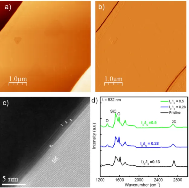
In collaboration with Dr A. Ouerghi from Laboratory of Photonics and Nanostructures (LPN-CNRS), we first looked at the nitrogen incorporation in trilayer graphene. Here the nitrogen was incorporated during the cooling process after the growth of the SiC sample, Fig.1.7.
Fig. 1.7 Schematic of trilayer graphene grown on SiC (a) grown under argon flux and (b) cooled under nitrogen flux37
Fig.1.8presents AFM, TEM images, and micro-Raman spectroscopy, obtained on the N-doped trilayer graphene sample. Fig.1.8(a) and (b) present the AFM images of the graphene grown on a SiC (0001) substrate. The AFM image shows a highly homogenous topography with a step density of 10–15 nm height and atomically flat terraces of about 7 𝜇𝑚 wide on average38 (Fig.1.8(a)). In AFM phase images (Fig.1.8(b)), at the step edges we observed the appearance of different regions, which corresponded to multilayer ribbons located at the very edge of the terrace39–41. As obser-ved from the STEM images (Fig.1.8(c)), the N-doped graphene produced here, is predominantly composed by trilayer graphene. In the STEM image, the 3C-SiC lattice planes are straight, sharp, parallel to the surface, and equidistant. The interlayer separation is about 0.34 ± 0.01 nm, and the graphitic layers are atomically flat and show a continuous film. In addition to acquiring AFM and STEM images, we characterized the graphene layer using Raman spectroscopy. In Fig.1.8
(d), typical spectra of pristine graphene and N doped graphene are shown, which correspond to measurements made on two locations of a terrace. The signatures of graphene are also observed as expected in the pristine and N-doped trilayer. They are identified by three main structures: (i) the D band, (ii) the G band, and (iii) the 2D band. For pristine graphene, the D peak is weak, indicating a low density of defects. In the case of N doped graphene, we note an increase of the D band and one more contribution due to the (D′) bands at 1620 𝑐𝑚−1, corresponding to the disorder-induced feature, which is known to occur in sp2 carbon with defects. The high intensity of D band, as well as the presence of the D band, suggests that nitrogen breaks the local symmetry
1.4 Modulation of the electronic properties of graphene 11
of the graphene lattice. In addition, we note that the 2D peak reduces in intensity and the FWHM increases from 40 𝑐𝑚−1to 70 𝑐𝑚−1as typically observed in N-doped graphene42.
Fig. 1.8 (a) AFM topography of N-doped graphene sample. (b) AFM phase image of N-doped graphene. Graphene layer covers the entire substrate. (c) Cross-sectional High-resolution STEM image of N-doped graphene. (d) Comparison of Raman spectra taken for different 𝐼𝐷/𝐼𝐺 ratios on N-doped graphene and comparison to pristine sample.43
In order to locate the nitrogen into the trilayer and measure the WF shift induced, we carried out XPS and UPS experiments. We probed the electronic properties of the samples using X-ray photoelectron spectroscopy (XPS) of nitrogen doped graphene layer (Fig.1.9). Fig.1.9(a) displays the deconvoluted C 1s core level XPS spectrum of N doped graphene. The C 1s spectrum sho-wed four components at 283.7, 284.6, 285.4, and 286.5 eV in binding energy. These components correspond to the SiC bulk (noted SiC), the graphene layer (noted G), the interface layer (noted IL), and the C-N bounds (C-N), respectively. The small new peaks at 286.5 eV suggest the bon-ding formation of doped nitrogen atoms to be sp2-C or sp3-C atoms. Fig.1.9 (b) shows the Si 2p spectrum for an N-doped graphene sample. It is dominated by a peak at 101.1 eV corresponding
to the bulk silicon and presents a shoulder at higher energies. The shoulder is composed of a peak at 102.0 eV assigned to the IL between the graphene and the SiC (0001) substrate. Another peak at 100.7 eV is attributed to Si clusters of broken Si-C bonds formed during the graphitization process. Fig.1.9 (c) shows the deconvoluted N 1s of the N-doped graphene sample. This peak is decomposed in three components centered at 398.2 eV, 399.6 eV, and 401.4 eV assigned, re-spectively, to pyridinic, pyrrolic, and graphitic configurations, rere-spectively, as shown in Fig.1.9
(d). It is admitted that graphitic-N is the most efficient doping configuration37,44. In our context, pyrrolic and pyridinic-N appear to be the dominant bonding configurations. Interestingly, no Si-N-C bonds are visible37. This observation indicates that the nitrogen is predominantly bonded in the graphene plane and edges and did not diffuse to the interface. This diffusion may have been prevented by the trilayer nature of the graphene in our sample.
We performed UPS analysis to determine the shift in work function induced by N atoms and verify the nature of the doping of graphene layers. As a reference, we utilized a sample of pristine monolayer graphene but without N-doping, the WF measured is 4.3 eV, similar values have been reported previously and trilayer undoped graphene is estimated to be 4.4 eV45. We therefore conclude that the N doping process implemented in this work on trilayer epitaxial graphene has demonstrated its effectiveness to shift to a minimum of 0.3 eV, the WF from 4.4 eV to 4.1 eV confirming the n-type nature of the graphene layer. The mobility for holes and electrons is about 1300 𝑐𝑚2/𝑉 𝑠 and 850 𝑐𝑚2/𝑉 𝑠, respectively measured on a top gate device with 𝐴𝑙2𝑂3gate oxide. The striking feature of this device is its carrier mobility that is nearly as high as pristine graphene obtained on Hall bars by Pallecchi et al.46 in prior work but at 4 K and without any gate oxide. We conclude therefore that although oxygen may have hindered the nitrogen doping to an extent, limited scattering or traps centers have diffused at the interface and the carriers mobility estimated could have been even larger before the gate completion. In addition, no hysteresis was observed while sweeping Vg back and forth indicating that no trapping occurred at the 𝐴𝑙2𝑂3/graphene interface. Note that current silicon high speed devices exhibit few 100 𝑐𝑚2/𝑉 𝑠 and suffer from short channel effects. Yet, considering the low on/off ratios logic devices are unrealistic however there is potential for radiofrequency FETs as the cut off frequency FT increases with mobility, but one should consider parasitic resistances to properly assess the potential for such applications. On the other hand, nanoribbons patterned on N doped graphene with optimized gate dielectric could open the band gap required for logic applications47. Such a scheme coupled to this atmospheric growth and doping method is a simple and cost effective approach to produce graphene based nanoelectronic devices.
1.4 Modulation of the electronic properties of graphene 13
Fig. 1.9 (a) C 1s spectrum for N-doped graphene. The deconvolution using Doniach-Sunjic line shape analysis shows the SiC, G, IL, and carbon nitrogen (CN) bonding configurations. (b) Si 2p XPS spectrum for N-doped graphene. (c) N 1s XPS spectrum for N-doped graphene showing 3 different nitrogen configurations. (d) The atomic configuration showing pyridinic-N, pyrrolic-N,and graphitic-N as well as graphene lattice and vacancies. XPS measurements were carried out at an angle of 45° with respect to the sample normal.
1.4.2
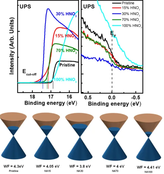
Ex situ doping by nitric acid
We have shown using in situ nitrogen doping that the WF could be modulated up to 0.3 eV. Here we have monitored the structural and electronic modifications of epitaxial graphene for different concentrations of diluted nitric acid (NA) 15 vol %(NA15), 30 vol %(NA30), 70vol %(NA70) and 100 %(NA100) of nitric acid (NA) solutions in deionized water (DI water) for 2min. The
electro-nic properties of the doped graphene samples were characterized by Raman spectroscopy and the work function shift after NA doping were measured using ultraviolet photoemission spectroscopy (UPS). To highlight the effect of nitric acid doping, these measurements were compared with the obtained values for pristine graphene. We demonstrated that the NA doping permits the WF modulation with respect to the dilution48,49. Indeed, the WF first increases the electronic doping between 15 and 30 vol %(NA15, NA30) and then decreases the electronic doping between 70 and 100 vol % (NA70, NA100). This study on epitaxial graphene presents striking differences compared to the work of Das et al on CVD graphene where only p-type work function shifts are observed. We clearly demonstrate that both systems react differently to an identical chemical functionalization. Morevoer, these observations are supported by density functional theory cal-culations (DFT)49,50, Fig.1.10. We believe that the first 𝐻𝑁𝑂3molecules dissociate and saturate
Fig. 1.10 (a) UPS data for pristine, NA30, NA70 and NA100 samples indicating the WF shift as a function of nitric acid concentration. (b) Illustration of the Fermi level shift in the graphene Dirac cones.
all available defect sites or step edges. This induces a nitrogen-doped graphene layer (NA15% and NA30%) and therefore decreases the WF. On the other hand, beyond NA30%, the 𝐻𝑁𝑂3 molecules can physisorb on the surface inducing a p-type doping, lowering the Fermi level and as
1.4 Modulation of the electronic properties of graphene 15
a result increasing the WF.
To evaluate the electronic quality of our graphene layers, we determined the carrier mobility of the pristine and NA100% doped graphene using van der Pauw measurements at room tempera-ture. Table 1 shows the electrical data measured for the pristine sample and NA100 extracted from Hall measurements. We have measured in previous works the electronic properties on such a monolayer graphene using the same growth mechanism. The lowest mobility achieved was 1400 𝑐𝑚2/𝑉 𝑠 at 300 K. Note that Günes et al.51 achieved a sheet resistance of 100 Ω/𝑠𝑞, using 𝐻𝑁𝑂3 doping on CVD graphene. These data clearly indicate that although doping alters the lattice of graphene to some extent, it does not render the material electronically poor. The orders of magni-tude are sufficient for many mainstream applications where contacts are required52–54, Fig.1.11∗.
Fig. 1.11 Electrical data extracted from Hall effect measurements on pristine and NA100% sample at 300 K, majority carriers are holes.49
1.4.3
CVD graphene/a-Si:H heterostructure
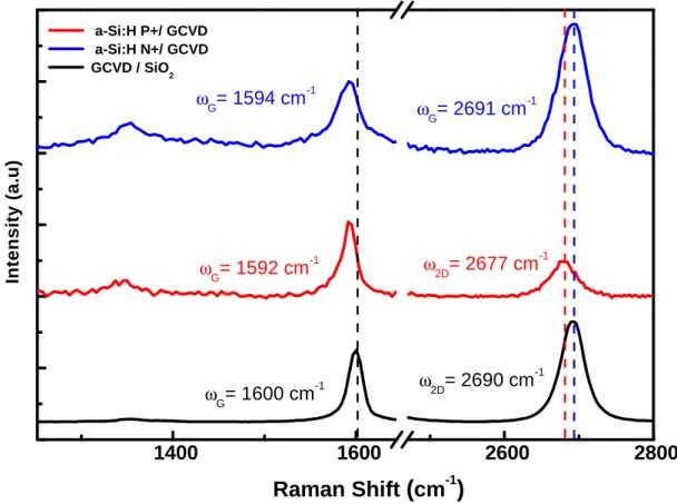
As we targeted to implement CVD graphene as a transparent electrode or a Schottky contact with crystalline silicon for solar cell applications56, we studied the impact of amorphous silicon (a-Si:H) onto monolayer graphene. a-Si:H is utilized as a passivation layer in silicon heterojunctions solar cells57. It prevents the surface recombination that is detrimental for the power conversion efficiency. To study the influence of a capping layer on the charge carrier transport in embedded graphene, 10nm of doped a-Si:H (n-type and p-type) were deposited onto the graphene by PECVD at 100 °C. Raman spectroscopy measurements have shown a difference between n-type and p-type a-Si:H doped silicon capped graphene. As deposited a-Si:H onto CVD graphene present a high compressive strain as observed in Fig.1.12. Interestingly, the Raman features of the embedded graphene are preserved and this clearly demonstrates that little or no structural damages occurred during the deposition process. Indeed the G peak downshifted for both n-type and p-type a-Si:H compared to pristine that is a signature of strain58. This red shift of both the G and 2D band is inherent to the elongation of the carbon-carbon bonds lowering their vibrational frequency. When n-type a-Si:H is capping the graphene, the shifts become - 6 𝑐𝑚−1and -1 𝑐𝑚−1for both the G and 2D peaks respectively whereas they increase to - 8 𝑐𝑚−1and -13 𝑐𝑚−1when p-type a-Si:H covers the graphene inducing more compressive strain. To elucidate a possible contribution of field ef-fect doping, Hall bars were patterned for transport measurements as a function of temperature to
1 4 0 0 1 6 0 0 2 6 0 0 2 8 0 0 ωG = 1 5 9 4 c m - 1 ωG = 1 5 9 2 c m - 1 ωG = 1 6 0 0 c m - 1 ω2 D = 2 6 9 0 c m - 1 ω2 D = 2 6 7 7 c m - 1 In te n s it y ( a .u )
R a m a n S h i f t
(
c m
- 1)
a - S i : H P + / G C V D a - S i : H N + / G C V D G C V D / S i O 2 ωG = 2 6 9 1 c m - 1Fig. 1.12 Raman spectra of CVD graphene capped with 10 nm a-Si:H p and n doped.
evaluate the sheet resistance, charge carrier density and Hall mobility of the encapsulated film59, Fig.1.13. We observe that whatever the capping type the electrical measurement are temperature independent, this is in sharp contrast with the observation of Gluba et al.60that observed the influ-ence of scattering mechansims for undoped capped graphene. In addition, we show that graphene capped with p-type a-Si:H undergoes a limited holes transfer increasing its charge carrier density without affecting its mobility (≈ 1400 𝑐𝑚2/𝑉 𝑠) compared to pristine on 𝑆𝑖𝑂2. Whereas the for n-type capping, the carrier density decreases and the mobility is reduced by more than a factor of 2 approximately with respect to graphene on 𝑆𝑖𝑂2(≈ 600 𝑐𝑚2/𝑉 𝑠 and Rs increased to 1300 𝑜ℎ𝑚/𝑠𝑞). As the strain is more important for p-type capping than for n-type and the defect peak does not substantially increase, the srain is not responsible for this change in transport properties. As a result, we conclude that there must be a field effect doping due to impurities at the interface. At last, we demonstrated that a phase change of the as deposited a-Si:H under high laser power induces a Raman shift61–64. The a-Si:H transforms into 𝜇 − 𝑐𝑆𝑖 for both type of capping as it is visible by the appearance of a peak at 520 𝑐𝑚−1, Fig.1.14. Both cappings exhibit up shifts for the G and 2D peaks upon crystallization inherent to the relaxation of the mechanical strain as well as a possible field effect doping as the intensity of the 2D peak diminishes as opposed to the G peak. We have demonstrated that the transport properties of capped graphene with a-Si:H remain interesting and the graphene is not damaged neither by the deposition process nor by the mechanical strain. This route may find application in embedded GFET channel to reduce the high
1.4 Modulation of the electronic properties of graphene 17
Fig. 1.13 Transport measurement versus temperature on CVD graphene capped with 10 nm a-Si:H : (a) sheet resistance, (b) mobility, (c) carrier density.
threshold voltage observed due to charge accumulation often due to contamination. The capping will prevent unintentional doping and tailor the Fermi level towards the charge neutrality point.
The Δ𝐸𝐹 can be evaluated with Eq.1.665.
𝐸𝐹 − 𝐸𝐷𝑖𝑟𝑎𝑐 = ℏ𝜐𝐹
1 2 0 0 1 6 0 0 2 0 0 0 2 4 0 0 2 8 0 0 4 0 0 4 8 0 5 6 0 ωG = 1 6 1 3 c m - 1 ωG = 1 5 9 4 c m - 1 ω2 D = 2 6 9 1 c m - 1
a - s i ( p ) / G r
c - s i ( p ) / G r
R a m a n S h i f t
(
c m
- 1)
ω2 D = 2 6 7 7 c m - 1I
n
te
n
s
it
y
(
a
.u
)
(a) 1 6 0 0 2 0 0 0 2 4 0 0 2 8 0 0 4 0 0 5 0 0 6 0 0 ωG = 1 6 0 4 c m - 1 ωG = 1 6 0 0 c m - 1 ω2 D = 2 6 9 5 c m - 1 ω2 D = 2 6 9 1 c m - 1a - S i ( n ) / G r
c - S i ( n ) / G r
R a m a n S h i f t
(
c m
- 1)
I
n
te
n
s
it
y
(
a
.u
)
(b)Fig. 1.14 Raman spectra of CVD graphene capped with 10 nm a-Si:H before and after recrystal-lization of the a-Si:H. a) p-doped, b) n-doped
1.5 Graphene/fluorographene heterostructures 19
Fig. 1.15 Energy band diagrams of heterostructures graphene/a-Si:H n and p doped. We estimate before crystallization a Δ𝐸𝐹 of 0.3 eV between the two capping type inherent to the charge transfer from the a-Si:H. However, this energy difference could also be inherent to metallic contamination such as 𝐹 𝑒𝐶𝑙3. It has been recently demonstrated that such heterojunction could exhibit power conversion efficiency up to 14-15 %66, Fig.1.15.
1.5
Graphene/fluorographene heterostructures
PhD student : Kuan-I Ho, thesis defended on january 12𝑡ℎ 2016 with Pr CS Lai at Chang Gung University (CGU). Funding Ministry of Science and Technology(MOST) - Taiwain . Subject : ”Study of Fluorinated graphene and its application for dielectrics and transistors”.
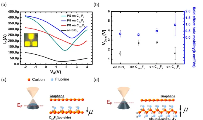
Since 2013, within the framework of the ICT-ASIA programme∗, I collaborate with Pr CS Lai of CGU on graphene based devices. The MOST has selected K-I Ho to carry out part of his PhD in France. In that context, he joind me from February 2015 to October 2015 to work on the integration of fluorographene (FG) as a passivation layer for FET device67,68. This technology has strong potential for 2D based nanoelectronic devices69,70. In this work, we presented a novel, fast, and efficient method to passivate silicon dioxide substrates (𝑆𝑖𝑂2) by forming FG on the substrate surface by 𝐶𝐹4plasma treatment. We studied the FG as a function of the 𝐶/𝐹 ratio and we observed that the fluorination process renders the graphene more hydrophobic and transforms the sp2 bonding configuration into sp3 configuration. We implemented these observations into the fabrication process of a self-aligned transistor where the gate was deposited at the last step as opposed to standard processes. Our gate-terminated self-aligned transistor further improves the overall performance by limiting the series access resistances and achieves a high carrier mobility ≈ 3000 𝑐𝑚2/𝑉 .𝑠, comparable to typical chemical vapor deposition graphene (CVD-graphene) on high quality self assembly monoloyers (SAMs) and on boron nitride (h-BN)71,72, Fig.1.16. Several devices have been tested to extract statistics. 𝑉𝐷𝑖𝑟𝑎𝑐errors bars on the different substrates are shown in Fig.1.16b, left axis. The 𝑉𝐷𝑖𝑟𝑎𝑐 of graphene on 𝑆𝑖𝑂2, 𝐶18.4𝐹1FG, 𝐶3.4𝐹1 FG, and 𝐶1.1𝐹1 FG are, respectively, 1.5, 2.5, 2.5, and 1.6 V. This trend indicates a p-type doping. We
observed that the leakage current is stable whatever the passivation and fivefold lower than the drain current indicating that the FGs do not present any leakage path. This is evidence of the insulating property of the FG layer. Surprisingly, the mobility improves as the 𝑉𝐷𝑖𝑟𝑎𝑐 increases with the fluorination, as opposed to usual trend observed elsewhere but in this work the FG acts as a passivation and is not the channel. Therefore one should consider the total electrostatic picture of the 𝑔𝑟𝑎𝑝ℎ𝑒𝑛𝑒/𝐹 𝐺/𝑆𝑖𝑂2 system, i.e., 𝑔𝑟𝑎𝑝ℎ𝑒𝑛𝑒/𝑑𝑖𝑝𝑜𝑙𝑒/𝑆𝑖𝑂2. In our study, both 𝑆𝑖𝑂2 and the graphene channel are identical for all samples and therefore should present the same charge impurities in 𝑆𝑖𝑂2, and charged or dipolar functional groups on graphene because of unintentional atmospheric contamination. These C–O based functional groups are known to be holes donors; they alter the local electric field on the graphene channel and therefore its conductivity. The graphene sheet exhibits a given electrostatic potential. This picture is the same for all our samples. However, once the FG passivation is introduced the electrostatic potential is perturbed and the presence or absence of a dipole moment at the FG/graphene interface will affect the charge transfer occurring through the FG/graphene/adsorbates system. In that regard, it has been demonstrated that the fluorination coverage translates into different F bonding configuration73–75 with C and therefore different dipole moment, 𝜇. For low F content, e.g., 𝐶4𝐹 , F bonds onto C preferably on one side, whereas for CF coverage, F covers all C atoms but on both side of the graphene sheet. For the later configuration that is close to our 𝐶1.1𝐹1FG, the opposite dipole moments cancel out. note that the C/F coverage is controlled by the fluorination time. Experimentally, we observed a ≈ 1 V increase in the 𝑉𝐷𝑖𝑟𝑎𝑐voltage for both 𝐶18.4𝐹1FG, 𝐶3.4𝐹1FG. These two FGs as opposed to 𝐶1.1𝐹1 FG present a dipole moment that facilitates the transfer of holes from the adsorbed contamination to the graphene sheet. This translates into a drop of the Fermi level (𝐸𝐹) in the graphene and as a result in an increase of 𝑉𝐷𝑖𝑟𝑎𝑐 as observed experimentally. Fig.1.16c illustrates the mechanism involved for the different dipole formation. On the other hand, the 𝐶1.1𝐹1 FG passivation that does not exhibit a net dipole, then the V Dirac is lower. Here, we believe that the absence of net dipole reduces the charge transfer from residual adsorbates and therefore little shift in the 𝐸𝐹 is expected as compared to 𝑆𝑖𝑂2. Indeed, no substantial variation of the 𝑉𝐷𝑖𝑟𝑎𝑐 is visible. The graphene (channel) is seen as decoupled from the 𝑆𝑖𝑂2 substrate through the 𝐶1.1𝐹1 FG passivation hence the better mobility. Note that the devices with FG passivation exhibit a higher slope, narrower minimum conductivity plateaus, and higher value of the minimum conductivity. This trend relates to a reduction of the scattering mechanisms and clearly indicates that the samples with FG passivation exhibit a lower charged impurity density. As shown in Fig.1.16b, right axis, the hole mobility of devices on FG is as high as three times enhanced for the lowest C/F ratio from 300 𝑐𝑚2/𝑉 𝑠 on 𝑆𝑖𝑂2to 1000 𝑐𝑚2/𝑉 𝑠 on 𝐶1.1𝐹1FG. The peculiarity of the 𝐶1.1𝐹1FG, i.e., C/F ≈ 1 is that all the fluorine atoms covalently bond to carbon atoms. We fabricated a gate-terminated self-aligned field effect transistor in order to reduce the access series resistances, Fig.1.17shows the electrical characteristics of the self-aligned graphene-FET with the 𝐶1.1𝐹1 FG passivation. The self-aligned process enhances the carrier mobility more than six folds from ≈ 300 𝑐𝑚2/𝑉 𝑠 on 𝑆𝑖𝑂2to 1800 𝑐𝑚2/𝑉 𝑠 on 𝑆𝑖𝑂2with self-aligned process. The introduction of the FG passivation further improves the mobility up to ≈ 3000 𝑐𝑚2/𝑉 𝑠. The FG passivation layer also induces a 50
1.5 Graphene/fluorographene heterostructures 21
Fig. 1.16 a) 𝐼𝐷𝑆–𝑉𝐺𝑆 characteristics of the top gate graphene-FET fabricated on FG substrate. The inset shows a photograph of the device under test. The scale bar in the inset is 50 μm. b) Comparative plot of the 𝑉𝐷𝑖𝑟𝑎𝑐 voltages and hole field-effect mobility as a function of the fluori-nation. c) Illustration of the dipole formation for 𝐶18.4𝐹1FG and 𝐶3.4𝐹1FG. d) Dipole formation for 𝐶1.1𝐹1FG. The black arrow indicates the orientation of the dipole moment 𝜇. The Dirac cones depicted show the variation of the Fermi level induced by the charge transfer76.
% enhancement in the drain current and an on/off ratio increasing from ≈ 2.4 𝑆𝑖𝑂2to 3 (𝐶1.1𝐹1 FG), Fig.1.17. We demonstrated that the FG passivation layer is a versatile and reliable option to improve the performance of graphene-based electronics∗. In February 2016, in collaboration with Chang Gung University and the Laboratoire de Photonique et Nanostructures (LPN-CNRS), I filed a patent application on the integration of graphene/fluorographene nanoribbons FETs for memory applications77.
Fig. 1.17 𝐼𝐷𝑆 – 𝑉𝐺𝑆characteristic of the devices fabricated with and/or without self-aligned design and 1 monolayer FG passivationho_selfaligned_2015.
1.6
International collaborative research
1.6.1 Toyohashi Tech - Japan - Graphene oxide
In 2012, I started a joint research on graphene oxide with Pr Adarsh Sandhu from the Electronics-Inspired Interdisciplinary Research Institute (EIIRIS) in Toyohashi University of Technology. In this work, graphene oxide was reduced into graphene through different chemical (hydrazine, ul-traviolet photocatalysis) and biological (microorganisms) processes78,79. We benchmarked the reduction efficiency of these methods by probing materials characteristics using X-ray photoelec-tron spectroscopy (XPS) analyses to observe the effectiveness of the reduction processes through the sp2/sp3 content. In addition, the homogeneity of the reduction was investigated on micrometer scale sample with micro Raman mapping as well as conductive-probe atomic force microscopy (CP-AFM) to investigate the longitudinal conductivity of the different samples. The results sho-wed that hydrazine based reduction remains the most efficient. However, the bacterial procedure demonstrated partial reconstruction of the carbon network and reduced the amount of oxygenated functional groups80. This work led to the signature of a Memorandum of Understanding between EIIRIS and UPMC.
1.6.2 Characterization of CVD graphene superlattices
Bilayer graphene (BG) has attracted attention thanks to its unique electronic structure, which can be modified by the stacking orders81–84. A tunable bandgap can be opened by applying verti-cal electric fields which break the layer symmetry with potential applications in photonics and electronics85. The CVD samples studies in this work were provided by Pr Y.Hee Lee group at
1.6 International collaborative research 23
Sungkyunkwan University South Korea. These samples presented peculiar flower-shaped struc-tures composed of bi and trilayer that exhibit random twist angles86,87. These peculiar structures could be interesting for graphene dot application or as a floating gate for nonvolatile memory. During our sudies on CVD graphene, we noticed the presence of multilayer defects across the
Fig. 1.18 AFM profile superposed to the optical image of 1L, 2L, 3L defect in CVD graphene. samples, Fig.1.18. These superlattices are composed essentially of bi and trilayer, Fig.1.19. We observed by TEM analyis and Raman that the twist angle is different for various structures within the same sample, Fig.1.20. Since the electronic properties in graphene are dependent on the num-ber of layer and stacking orientation, we decided to probe these features on our samples by Raman spectroscopy, and nano - Angle Resolved Photoemission Electron Spectroscopy (ARPES) at sy-nchrotron Soleil.
Fig. 1.19 (a) optical image of trilayer graphene superlattices, (b) Raman mapping of the 2D band, (c) Raman mapping of the G/2D ratio, (d) Raman spectra for different twist angles.
Fig. 1.20 (a) Fourier transform HR-TEM of 1ML CVD graphene.(b,c,d) diffraction of bi and tri-layer CVD graphene exhibiting various twist angles.
1.6 International collaborative research 25
1.6.3 Synchrotron Soleil collaborative research - nanoARPES
In the continuity of the GraPhIC project, GeePS and ANTARES beamline have initiated a col-laboration to investigate various combination of material at synchrotron Soleil under proposal 20140653 entitled Chemical nano-imaging and detection of density of states close to the Fermi level on multilayers graphene islands and heterojunction. In particular, I was interested in pro-bing the band structure directly onto the aforementioned superlattices88,89. Our collaboration is
Fig. 1.21 (a) Optical and SEM picture of a Hall bar patterned onto a twisted bilayer graphene, (b) 𝜌𝑥𝑥and 𝜌𝑥𝑦as a function of the magnetic field.
on-going with a focus on heterojunctions. Notably, I am particularly interested in probing the charges trapped at an interface after injection through a tunnel barrier.
1.6.4
Tokyo Institute of Technology - Japan - Spatio-temporal observation
of photogenerated electron dynamics in graphene superlattices
In the last decade, graphene has been one of the most studied 2D materials. Quasi-standing mono and multilayer graphene has attracted attention for a range of optoelectronic applications. The mo-dulation of graphene’s properties for devices applications relies on the understanding of the carrier interactions and recombination dynamics95,96. Indeed, stacked monolayer graphene, demonstra-tes tunable band stuctures that depends on the stacking orders, i.e. the rotation angles between two layers. Therefore, understanding the ultrafast kinetics and their correlation with the num-ber of layers as well as the stacking configuration is of particular interest. However, the ultrafast carrier dynamics influenced by the crystallographic structures is not well understood, because of the instrumental limitations. Here we utilize a different technique coupling an optical pump-probe technique using femtosecond laser pulses and a photoemission electon microscopy with the spatial resolution of 100 nm (time-resolved photoemission electron microscopy97,98: fs-PEEM),Fig.1.22. On one hand the fs timescale helps to investigate the faster relaxation mechanisms, and on the other hand the simultaneaous microscopic observation probes any particular region that may exhibit a
given rotation angle. These relaxation mechanisms have been extensively studied in high quality exfoliated and SiC graphene using pump probe techniques99. For our superlattices, we estima-ted the photogeneraestima-ted carrier lifetimes in selecestima-ted regions has been estimaestima-ted by time-resolved photoemission electron microscopy with 100 nm spatial and 100 fs temporal resolutions.
Fig. 1.22 (a) Illustration of the sample investigated in the PEEM system, (b) pump laser at 4.8 eV excites electrons from the valence band to the conduction band of the graphene the relaxation is probed at 1.55 eV.
Our spatial resolution permits to acquire in one shot the photoemission of all these superlatti-ces. A subsequent analyzis performed on the pixelized image allows the extraction of the lifetime of the carrier within a particular region. As a result, we are able to produce a map of lifetime accross a large scale graphene sample and establish the superlattices which have a stronger inte-raction with the underlying substrate and other which seem decoupled from the substrate. Fig.1.23
a shows a the Raman microscopy image of the 2D peak over the G peak to enhance the structu-ral information. The bilayered regions correspond to a rotation angle of > 12°, 12° and < 12°, respectively. These angles have been determined from the Raman signatures.
Fig. 1.23 (a) Raman mapping of G/2D bands of different superlattices with twist angle : < 12°, = 12° and > 12°, (b) PEEM intensity image corresponding to the same regions.
Fig.1.24(a) provides a PEEM image obtained at the same region to Fig.1.24(b) in addition to monolayer region, Fig.1.24. Slightly darker contrasts in the three regions indicate the higher
work-1.6 International collaborative research 27
Fig. 1.24 (a) Raman spectra of different superlattices with twist angle : < 12°, = 12° and > 12°, (b) PEEM intensity profile as a function of time for the 3 superlattices.
functions inherent to the different stacking orders. From the PEEM intensity, we can determine the lifetime of the photogenerated carrier for each angle, Fig.1.24. Different stacking orientation give rise to a different band structure and therefore we expect a different recombination lifetime for each region. Clearly, we observe a difference between the monolayer that is directly onto silicon dioxide and suffers from phonon interaction as opposed to the bilayer superlattices. These latest appear to be decoupled from the substrate and longer lifetime are observed. The PEEM system presented here is able to precisely mapping in space and with fs time resolution the lifetime of photogenerated carrier in complex nanostructred materials. We are currently accumulating more data on these samples and extended our study to topological insulators (submitted to Carbon).
1.6.5
Chang Gung University - Taiwan
1.6.5.1 Graphene nanodiscs nonvolatile memory
Since 2013 in the framework of the ICT-ASIA project , I collaborate with Pr CS Lai in Chang Gung University (Taiwan). He has been engaged in the research of the characterization and reliability of MOSFETs, flash memory, high-k dielectrics and biosensors. In that context, we worked on SiC and CVD graphene FET device for memory applications43,76,77. With regard to graphene, its large scale synthesis by chemical vapour deposition (CVD) and its transfer process onto functional substrates have opened new opportunities for device integration. However, the growth as well as the transfer of the material inherently generate structural and electrical defects. Although defects are usually detrimental for most of the devices operation, it is possible to exploit them as a trapping centres i.e. charge storage nodes for the fabrication of atomically thin films non-volatile memories (NVMs)100–103, Fig.1.25. In this work, we have integrated graphene nano discs (GNDs ≈ 20 nm)
Fig. 1.25 a) illustration of the energy band diagram at the flat band. a) programme operation, the electron tunnel through the 3 nm SiO2 barrier. This results in a Fermi level located in the conduction band. c) erase operation, the electrons tunnel back and the Fermi level move down into the valence band.
as charge trapping nodes for non-volatile memory (submitted to Carbon). The fabrication process relies on the patterning of Au nanoparticles (Au-NPs) which thicknesses are tuned to adjust the GNDs diameters upon etching. A density of GNDS as high as 8𝑥1011𝑐𝑚−2 is achieved. The functionalization of the GNDs by 𝑁𝐻3plasma introduces defects sites and 𝑁 − 𝐻+and 𝑁 − 𝐻2+ functional groups as observed by Raman and FTIR spectroscopies. This inherently enhances the density of the trapping centers in and around the GNDs. As a result, the memory window reaches more than 2.4 V and remains stable after 104 operating cycles. The charge loss is less than 10 % 10-year data retention rendering this simple back end process suitable for low cost nonvolatile memory∗, Fig.1.26.
1.6 International collaborative research 29
Fig. 1.26 GND nonvolatile memory characteristics. (a) P/E characteristics without NH3 functi-onalization. The gate voltage (calibrated by initial 𝑉𝐹 𝐵) is 8 V for programming and -8 V for erasing, with 10−6 s to 1 s pulse width. (b) P/E characteristics after 𝑁𝐻3functionalization. The memory window significantly enhances. (c) The endurance characteristics of the 𝑁𝐻3 GND-NVM. The samples can sustain more than 104cycles with +/−8 V for P/E operation. (d) Extra-polated data retention characteristics of the GND-NVM. Less than 10 % charge loss after 10-year is expected.
1.6.5.2 Multilayer graphene nanoribbons
We already mentioned in section 2.5 our work on fluorographene and its potential as a passivation layer. In this collaboration, we present a novel graphene nanoribbon (GNR) transistor fabricated by the partial fluorination of the channel. This fully back end process permit the design and the fabrication of FinFet like GNR, Fig.1.27.
Our heterostructre consists of directly embedding the tunnel dielectric within the multilayer graphene i.e.partial transformation of the graphene by fluorinated plasma instead of growth or de-position process. Our first attempt showed that the ambipolar behaviour on GNR can be achieved with such process with a reasonably low gate nA leakage current, Fig.1.28. Interestingly, a few