~n
;A r lrr^-> , ;-rl_ L N T
ROOM
36-412 ,~' t nl Sr
-~~~nr
i
WITH
S
E
FEUN
CA
TESI
i
r 4 > i o
) lt...Ur
..
i6
I tv J:sos?', f5a ,!ls.tr''j'6 11 8^,t~~~ 0t-,,'
w
AAPLIFIERS WITI-
`PRSAIBED
FREQUENCY CHARACTERISTICS
AND ARBITRARY BANDWIDTH
JOHN G. LINVILL
copor
TECHNICAL REPORT NO. 163JULY 7, 1950
RESEARCH LABORATORY OF ELECTRONICS
MASSACHUSETTS INSTITUTE OF TECHNOLOGY CAMBRIDGE, MASSACHUSETTS
t
The research reported in this document was made possible through support extended the Massachusetts Institute of Tech-nology, Research Laboratory of Electronics, jointly by the Army Signal Corps, the Navy Department (Office of Naval Research) and the Air Force (Air Materiel Command), under Signal Corps Contract No. W36-039-sc-32037, Project No. 102B; Department of the Army Project No. 3-99-10-022.
This report is based on a thesis in the Department of Electrical Engineering, M.I.T.
MASSACHUSETTS INSTITUTE OF TECHNOLOGY RESEARCH LABORATORY OF ELECTRONICS
Technical Report No. 163 July 7, 1950
AMPLIFIERS WITH PRESCRIBED FREQUENCY CHARACTERISTICS AND ARBITRARY BANDWIDTH
John G. Linvill
Abstract
The amplifier chain, a cascade connection of amplifier tubes connected by two-terminal or two-two-terminal-pair interstages, is the basic component of the amplifiers designed. Shunt capacitance in the interstages imposes a limit on the amplification per
stage over a prescribed band of frequencies. The limit of amplification per stage is inversely proportional to the bandwidth. The method of design of amplifier chains
pre-sented leads to simple interstages which are economically close to the maximum in performance for the shunt capacitance present. The interstages used are simple-tuned circuits or double-tuned circuits. The technique of design of the amplifier chains is related to the stagger-tuning technique invented by Wallman. The characteristics of
individual stages are nonuniform but the stages in a chain complement each other to provide an acceptably uniform characteristic. In the design procedure one chooses the amplification function for the chain being designed, according to a flexible technique presented in Technical Report No. 145, such that prescribed frequency characteristics are approximated. The amplification functions so chosen are suitable to be identified with realizable networks. This step is the key of the whole design process.
Single amplifier chains become ineffective as amplifiers when the bandwidth becomes so broad that the amplification per stage approaches one. When amplifiers are to
amplify such broad bands of frequencies that this situation arises, more than one ampli-fier chain is used. The chains amplify different sub-bands and are connected in parallel at the input and output. The amplification functions of the individual chains are so chosen that the chains, when connected in parallel, give a desired characteristic.
A summary of the pertinent characteristics of the distributed amplifier (invented by Percival), which is capable of amplifying over bands greater than those for which single amplifier chains are useful, permits a comparison with the parallel-chain amplifier. The parallel-chain amplifier is more economical in tubes and the design is more flexible. The frequency selectivity of the parallel-chain amplifier is affected by nonuniform
changes in the tube characteristics; a properly designed distributed amplifier has a frequency selectivity not altered by changing transconductances of the tubes.
-AMPLIFIERS WITH PRESCRIBED FREQUENCY CHARACTERISTICS AND ARBITRARY BANDWIDTH
1.00 Introduction
The design of vacuum tube amplifiers is a broad subject because of the diverse uses of amplifiers and the widely different specifications on performance in different applica-tions. The majority of design specifications include a prescription for the frequency characteristics of the amplifier to be designed. Ordinarily the frequency character-istics, the magnitude of amplification and the phase shift over the band of frequencies amplified, are the primary specifications for the amplifier. Further specifications may be viewed as added requirements or constraints. The technique of design of amplifiers can logically be based around a procedure for realizing amplifiers with prescribed fre-quency characteristics. This report presents such a procedure that is simple and flexible. The basic building block in the design procedure is the amplifier chain - a conventional cascade connection of amplifying tubes which are connected by simple two-terminal or two-two-terminal-pair interstages. For very broad band amplifiers two or more amplifier chains are connected in parallel; each amplifier chain amplifies a smaller, suitably chosen sub-band of the total band of frequencies being amplified.
The basic limitation which restricts the level of amplification obtainable in a given amplifier over a given band of frequencies is the shunt capacitance associated with the tubes and interstages. Parasitic capacitance is inevitable. The designer is accordingly obliged to furnish designs, with a minimum of parasitic capacitance, which give as large amplification as is feasible with the amount of capacitance present. Simple
inter-stages are desirable in that the parasitic capacitance introduced is smaller than that introduced in complicated circuits. Moreover, simple circuits are easy to build and
adjust. Circuits designed by the procedure presented here are simple and give very good amplification for the amount of shunt capacitance present.
1. 10 Summary of Previous Contributions
Previous contributions in the field of amplifier design which have particular signifi-cance for the method presented here are divided into two classes. One of these classes includes contributions dealing with the nature of and a quantitative evaluation of the limit imposed by shunt capacitance. The second class of contribution deals with design tech-niques which have been developed earlier for various kinds of amplifiers.
1. 11 The Limitation Imposed by Shunt Capacitance
The most familiar example illustrating the limitation of shunt capacitance on ampli-fier performance is the RC two-terminal interstage shown in Fig. la. The band of fre-quencies over which a stage of amplifier using this interstage has less than half-power variation in amplification is 1/RC rad/sec and the maximum impedance which the circuit presents is R ohms. If one wishes to obtain a larger bandwidth with this circuit, he
-1-must lower R and hence the amplification. To design a better stage one should try to find a circuit of the nature of Fig. lb in which the driving-point impedance can be
main-tained over a corresponding bandwidth at a larger value than is possible with the RC circuit. A large number of circuits were proposed to do specifically this thing long before an analysis was completed to show the fundamental nature of the limitation imposed by shunt capacitance on the impedance level.
Several writers have suggested circuits, but Wheeler (1) made a comprehensive study of the problem and suggested a number of filter circuits which, used as interstages, would give a better amplification over a prescribed band of frequencies than could be achieved with the simple RC circuit. Wheeler stated, on an empirical basis, that the maximum uniform impedance which could be maintained over wo rad/sec in a network with a shunt capacitance C is 2/C° o ohms, which is twice the impedance level of an RC
network with an wo rad/sec bandwidth. This limit is obtained with filter circuits requiring an infinite number of elements.
2 2
(a) (b)
Fig. 1 Simple two-terminal cir- Fig. 2 A two-terminal-pair network with cuits with shunt capacitance. shunt capacitance at the terminal pairs. Subsequent analytical work by Bode(2) verified the conclusion stated by Wheeler. Bode's work was essentially to determine the maximum constant magnitude of a driving-point impedance over wo rad/sec if this impedance must approach 1/XC (X is the complex frequency variable) as X approaches infinity. The prescribed behavior of the function at infinity in combination with the restriction to positive real character* limits the maxi-mum uniform magnitude over wo rad/sec to 2/o C ohms and Wheeler's empirical result was substantiated on analytical grounds.
The problem of evaluating the limits imposed by parasitic capacitance in the case of two-terminal-pair networks was treated by both Wheeler and Bode. In Fig. 2 is shown a two-terminal-pair network with equal shunt capacitances whose limiting behavior can be compared with the limit obtainable with networks of the form Fig. lb. The analytical problem solved by Bode was to determine the maximum uniform level of transfer imped-ance over wo rad/sec for such a circuit. This he determined to be 2/2W C ohms. One can say, on this basis, that splitting the shunt capacitance into two equal parts increases the potential effectiveness of a stage by 2. 47 times.
The foregoing discussion applies specifically to single-stage amplifiers. Most practical cases involve amplifiers of several cascaded stages. The results stated above *A positive real function of X is a rational function of X whose real part is never nega-tive for posinega-tive values of the real part of X. Posinega-tive real character is the necessary and sufficient condition that a function be the driving-point impedance of a physically realizable passive network.
-2-apply only to multi-stage amplifiers in which the amplification of every stage is uniform over the pass band. Hansen (3) determined the limit of amplification in amplifiers with a uniform over-all characteristic but with individual stages having nonuniform character-istics (stagger-tuned amplifiers). He found that for two-terminal-pair interstages the
stagger-tuned case offers a slight advantage but that for two-terminal interstages the limits are the same as for the case of identical stages each with uniform amplification
over the pass band. 1.12 Design Techniques
Most previous contributions in the techniques of design of amplifiers consisting of a single chain were centered around improvement in the characteristics of the RC amplifier. The use of inductance in shunt with the parasitic capacitance at the terminal pairs of the interstage or in series between the ungrounded terminals of the input and output (called respectively shunt and series compensation) is the most familiar artifice for improving the amplification-bandwidth product of the RC amplifier. This method results in a very simple circuit. The choice of parameter values is usually made either empirically or analytically to suit the particular application. The filter interstages sug-gested by Wheeler, which were mentioned in the last section, are theoretically more effective but also much more complicated. In practical circuits these interstages are seldom used. Experience establishes the principle that simplicity of a circuit is fre-quently as necessary as it is practically convenient. A complicated circuit ordinarily possesses more shunt capacitance because of its complication; consequently, its greater effectiveness in approaching the limit imposed by shunt capacitance is largely cancelled.
In many amplifiers it is necessary to employ more than one stage to obtain the desired level of amplification. The cascading of identical stages to achieve a higher level of amplification is a method commonly used. It possesses two obvious flaws which become more serious as the number of stages increases. In the first place, the pass band shrinks in width. This is easily appreciated through observing that the half-power frequencies of a stage are the quarter-power frequencies of two such identical stages connected in cascade. The half-power frequencies of the two-stage amplifier are closer together than these quarter-power frequencies. The second flaw is that irregularities in the level of amplification in the pass band are accented as the number of stages increases. For example, a ten-stage amplifier composed of identical stages which gives an amplification uniform over the band to within 30 percent must possess individ-ual stages which are uniform to within 2.7 percent. The requirement of such extreme uniformity necessitates an undesirable complexity in the interstages or excessive shrinking of the bandwidth. A novel and extremely practical alternate solution to the problem of the design of a multi-stage amplifier is that of stagger tuning suggested by Wallman (4). A simple form of stagger-tuned amplifier is shown in Fig. 3. Each stage is tuned to a slightly different frequency and has a different damping. It turns out that an appropriately chosen set of nonuniform characteristics leads to an acceptably uniform
over-all characteristic. The interstages are remarkably simple and fortunately such an amplifier provides an amplification level which is acceptably close to the limiting level
set by the shunt capacitance. Wallman (4) and Baum (5) have given methods whereby one can select the tuned frequency and damping of the individual stages to give certain simple desirable over-all characteristics.
Ei;
i
---
I
E,Fig. 3 Equivalent circuit of stagger-tuned amplifier.
IN
Fig. 4 Circuit of Percival's amplifier.
By the methods just discussed one can design an amplifier consisting of a chain of cascaded stages which will provide any amplification if the bandwidth is not so broad that the amplification per stage is forced down to one by the shunt capacitance. As the bandwidth required approaches this critical limit, the method of cascading to increase the amplification becomes less effective and finally fails. The theoretical problem of designing an amplifier which exceeds the bandwidth possible for conventional amplifiers has been solved before in only one way. Percival's amplifier (6, 7, 8), in which the grids and plates of vacuum tubes are distributed along two artificial lines, gives (theoretically, at least) any amplification over any bandwidth. The Percival amplifier is so constructed that the transconductances of its tubes are essentially summed without incurring an added loss due to increase in parasitic capacitance. This fact frees it from the kind of amplification-bandwidth limitation applying to single chains of cascaded amplifiers. Its operation is explained through consideration of Fig. 4. A signal applied at the input is propagated down the grid line, actuating the tubes in succession. Each of them injects a
current into the plate line, and the current wave is reinforced at each tube; its size at the output is determined by the number of tubes along the line. The shunt capacitances of the transmission lines are identified with the parasitic capacitances of the tubes. To get amplification over a wide band, one designs the lines with a suitably high cut-off
frequency. Increasing the cut-off frequency always reduces the impedance level of the transmission line and thereby reduces the amplification for a given number of tubes. Hence in the Percival amplifier (called the distributed amplifier by Ginzton (7), parasitic
capacitance still limits the amplification-bandwidth product though it does not put a theo-retical limit on the breadth of the band of frequencies to be amplified. By choosing a sufficient number of tubes for each stage (Fig. 4) and connecting a suitable number of such stages in cascade, one can theoretically obtain any level of amplification over any bandwidth. The disadvantages of the distributed amplifier are the inflexibility of the design (all sections of the lines must be identical, and the lines must be properly termi-nated) and the expense in the number of tubes required for a given performance. If there is much parasitic coupling between the two lines, the resulting feedback will cause insta-bility. The amplifier has the advantage that the frequency characteristics are not
influ-enced except in level by changes in the transconductances of the tubes.
The method, described later in this report, of paralleling simple amplifier chains, each effective over a fraction of the bandwidth, has been suggested before (9, 10) but it has never been made workable by a suitable design procedure.
1. 20 New Technique of Amplifier Design
The technique of amplifier design presented here is applicable both for narrow- and broad-band cases which require respectively one chain and a number of paralleled chains. In either case the single amplifier chain is the basic building block.
A typical amplifier chain is shown in Fig. 5. For such an amplifier chain the ampli-fication function is
E
E ( - g m) Zil ZiZ Zin( ( g n Zo)n (1)
i
In Eq. 1 Zill Zi2 . . . Zin are the interstage impedances. They are driving-point imped-ances if the interstages are two-terminal networks, transfer impedimped-ances if the inter-stages are two-terminal-pair networks. In either case shunt capacitance always appears at the pairs of terminals.
INPUT OUTPUT
TWO-TERMINAL INTERSTAGE TWO-TERMINAL- PAIR INTERSTAGE
Fig. 5 Amplifier chain and typical interstages. E
Amplification function of the chain is o () . Ei
1
In a broad-band amplifier requiring more than one chain, one prescribes the individ-ual amplification functions to be of such nature that the amplification function of the complete amplifier (the sum of the amplification functions of the paralleled chains) has the desired properties. Figure 6 shows typical amplification characteristics of a two-chain amplifier.
The salient quantities upon which attention is centered throughout the design pro-cedure are the amplification functions of the individual chains. The magnitude and
IAMPI " CHARACTERISTICS
/' /OF INDIVIDUAL CHAINS
FREQUENCY -Fig. 6 Typical amplifier
character-istics of two-chain amplifier.
In either the single- or multiple-chain choice of the amplification functions of the be suitable to identify as the amplification
argument of the amplification function for real frequencies are the frequency character-istics of the amplifier chain. The interstage impedances are factors of the amplification function. For the interstage types used
(Fig. 5) these impedances are simple functions. Element values of the interstages are easily
related to the amplification function. Design constraints in the amplifier are readily trans-lated into constraints on the amplification function. For instance, in an n-stage ampli-fier with two-terminal interstages each with
shunt capacitance C, the amplification function is constrained to approach (- gm)n/(XC)n as X approaches infinity.
cases the key to a successful design is the individual chains. The functions chosen must functions of the amplifier networks to be real-ized, they must provide the frequency characteristics desired and the level of amplifica-tion in the individual chains must be economically close to the limit set by the shunt capacitance. This key problem in the design procedure, the choice of a function approxi-mating prescribed magnitude and phase characteristics, is a familiar one which appears in almost all network design problems and is called the approximation problem. In the previously developed design methods for stagger-tuned amplifiers (4, 5) this problem was solved implicitly despite the fact that the approach was from a different point of view. A moment's reflection upon the approximation problem as viewed here in connection
with Eq. 1 indicates that what one is doing here is really closely related to stagger-tuning. Through solving the approximation problem one selects Z both to ensure that Z0, the
desired frequency characteristics of the amplifier, will be obtained and to ensure that ZO is factorable into realizable interstage impedances. The process automatically allo-cates to the various stages characteristics which are complementary in a sense similar to that in which the individual stage characteristics of Wallman's amplifiers are
comple-mentary. Here we find a desirable amplification characteristic which is factorable into realizable stage characteristics while the view previously taken is to find realizable
-6-I01'1
stage characteristics which combine to give a desired over-all amplification character-istic. The approach taken here, the choice of the amplification functions of the individual chains, is adapted to a solution of the approximation problem which is presented in a companion report (11). This report gives a method whereby one can obtain rational func-tions whose magnitude and argument approach desired characteristics over the range of interest of the frequency variable. The procedure of solution is to start with a trial set of positions of poles and zeros of ZO (Eq. 1). The trial set of pole and zero locations are constrained to lead to the type of network of interest. The frequency characteristics corresponding to this trial set of locations only roughly approximate the prescribed fre-quency characteristic. The trial set is chosen from experience with related problems or purely on the basis of a set of characteristic curves given in the report. Observing the deviations of the characteristics of the trial set from the characteristics desired, one shifts the location of poles and zeros from the first trial position to a second trial posi-tion by a systematic procedure. The shift is such that the constraints imposed earlier to lead to realizable networks are not violated, and the frequency characteristics are improved. The whole process is a systematic fitting procedure of unusual flexibility which one continues until the resulting deviations are tolerable. For most practical problems the procedure is simple and brief. For precise approximations a more com-plicated but more powerful algebraic fitting procedure is presented which gives results obtainable by no other known method.
As is apparent later when the problem of paralleling chains of amplifiers is discussed in detail, the practical constraints which must be imposed on the form of amplification functions of the chains makes the flexible solution to the approximation problem the most important key in the success of the design procedure presented.
2. 00 The Design of Amplifier Chains
The design of the basic building block of the amplifier, the amplifier chain, Fig. 5, proceeds most effectively when the basic limitation to its performance, the shunt capaci-tance, is precisely understood. The following development specifically defines the amplification-bandwidth limitation imposed by parasitic capacitance on amplifier chains. Following the development, a design procedure is presented for amplifier chains in which shunt capacitances appear.
2. 10 The Limitation Imposed by Parasitic Capacitance for Two-Terminal Interstages The presence of parasitic capacitance is always most directly apparent in the behav-ior of the circuit at high frequencies. If the network is a two-terminal network, as shown in Fig. 7, the driving-point impedance must approach 1/CX and become zero as infinite frequency is reached, regardless of what other passive elements are connected in the box. Moreover, the driving-point impedance Z must be a positive real rational
-7-function*. The pertinent question with regard to the amplification-bandwidth limitations is: Does the behavior of Z at infinity along with its positive real character impose a limit on the level of magnitude of Z over a prescribed frequency range ? The answer is yes.
The relationship which makes the limitation most evident is an application of Cauchy's theorem. Cauchy's theorem proves that the integral of a function around a closed con-tour is zero if the concon-tour encloses no singularities of the function. The positive real
character of Z insures that Z has no poles in the right half-plane. If one considers a contour bounding a large semicircle in the right half of the X-plane (Fig. 8), Z is analytic inside the semicircle. As the radius of the circle is permitted to approach infinity, the value of Z on the circular part of the contour approaches 1/XC. Any analytic function of Z integrated over the contour shown in Fig. 8 will give zero, the component of that integral on the semicircle being dependent upon C. By choosing the proper func-tions of Z to be integrated in this matter, illuminating results on the implicafunc-tions of parasitic capacitance can be deduced. Bode has given a number of results arrived at on this basis. One of them is that the largest uniform level of magnitude of Z (Fig. 7) over Wo rad/sec is 2/Cco0 ohms.
Fig. 7 Two-terminal impedance with parasitic capacitance.
IMAGINARY
X- PLANE
REAL
Fig. 8 Contour in X plane.
Attention will be turned back to Eq. 1 and Fig. 5 for the case in which every interstage is a two-terminal network. Stated in the most convenient terms, the problem is: What is the maximum constant magnitude of Z which can be maintained fixed from zero to co rad/sec in view of the fact that the factors of Z must be positive real functions approaching 1/XC as approaches infinity ?
The answer is most conveniently obtained through consideration of a relationship developed by Bode (12) which applies to Zil, Zi2 . . . or Zin in Eq. 1. For a typical one of the impedances, one has Eq. 2.
a. lp d __ + o / o o ip 2 X r 1 I 0 2 CWi ip
*A positive real function of X satisfies these qualifying conditions: ReZ > 0 if Re > 0, Im Z = 0 if Im X = 0.
-8-1
Equation 2 was developed by Bode through the integration of
in o \
around the contour in the complex frequency plane shown in Fig. 9. Since IPip can never exceed 1T/2 radians for X = jw (Zip being a positive real function), the second integral of Eq. 2 must not be negative and can only be zero in the limiting case in which pip =- T/2 for w > o0.
NE Fig. 9 Contour around which
l(IlZ + + X) CZ
in 2 2 is integrated to obtain Eq. 2.
J _o)
If one writes a set of relationships of the nature of Eq. 2 and sums them for all factors of Zo, Eq. 3 results.
n I n i ip
Cp w W Pi+2 ip c irn 2
LE
3
J d---- + d - in (3)()2 0o 2 o 2 C
The first integral of Eq. 3 is recognized to be
in
IZo
dXo / oj
Clearly, this integral will be a maximum if the second integral of Eq. 3 is zero, as the second integral cannot be negative. This fact means that beyond oo rad/sec every inter-stage impedance should be a pure capacitive reactance if the magnitude of amplification up to Wo rad/sec is to be maximized. The maximum constant level of IZo is given by Eq. 4.
I
d = ' in ·nmxd Zo T In () n (4)o
1 0 2oo
Equation 4 reveals that Zo I max is (2/Coo) n ohms.0
Equations 2, 3, and 4 all apply to cases in which the amplifier involved is of the low-pass type. That precisely the same limit applies to band-low-pass cases can be proved by use of a different integrand evaluated around a contour similar to that shown in Fig. 9. The integrand involves branch points at the edges of the band instead of at + jo and the
algebraic manipulations are more complicated.
The result expressed in Eq. 4 indicates that the limit of uniform amplification of n stages is just the nt h power of the limit of uniform amplification of a one-stage ampli-fier. In the proof just outlined the individual interstage impedances are not assumed to have uniform levels of impedance to w0 rad/sec. The attainment of the limit requires only that the stages acting together provide uniform amplification over the pass band and have the maximum phase shift consistent with physical realizability beyond the pass band. At this point, one first appreciates that the method of getting a wide-band ampli-fier of cascaded stages through making every stage equally good and equally flat is unnecessary. This erroneous idea seems to have been widely held before Wallman's
stagger-tuned amplifiers.
According to the results indicated in the foregoing discussion, the level of ampli-fication over 0o rad/sec which cannot be exceeded by an n-stage amplifier with
two-terminal interstages is (2gm/C 0o)n.
2. 11 Simple Amplifier Chains With Two-Terminal Interstages
The analysis just given establishes the upper limit of amplification set by parasitic capacitance, but gives little indication as to how close to that limit one can reach with practical networks. A design method for a simple low-pass amplifier gives an indication of the possibilities practically attainable. The two-terminal interstages of the design
presented include both single-tuned circuits and RC circuits. For this design method the amplification is not exactly uniform; it exhibits equal maxima of deviation in the pass band. For half-power variations, the level of amplification is 50 percent of the
theo-rectical limit. Accordingly, for 10 percent variations the amplification level over a band w0 rad/sec wide is 0. 242 (gm2/Co0)n. For an n + 1 stage amplifier, the
ampli-fication level is 0. 242 (gm2/Cwo)n+l. This result is rather interesting, in that it means that an n + 1 stage amplifier gives an amplification of an n-stage amplifier times the theoretical limit for one stage. The effectiveness per stage for a given tolerance on uniformity in the pass band increases with the number of stages.
The simple case presented also is used to illustrate the problems of design of an amplifier chain. The design of an amplifier chain can be divided into two parts: the approximation problem and the network realization. The approximation problem for this simple case is discussed first, and the network realization is taken up last. 2.12 The Approximation Problem for a Simple Amplifier Chain
The approximation problem, the problem of choosing a rational function which can be identified with Zo, is logically attacked in two steps. The first step is the selection
-10-of a class -10-of rational functions which satisfy the conditions -10-of physical realizability -10-of ZO and are adapted to identification with the product of simple driving-point impedances. The conditions of physical realizability of ZO are that it be the ratio of Hurwitz poly-nomials, that it approach 1/(Ck)n as X approaches infinity, and that
[Arg Zla n2
The second step is the selection from the chosen class of functions of a type which exhibits a large approximately constant magnitude in the range of real frequency, zero to Wo rad/sec, with an argument approaching - n ir/2 beyond oo .
To proceed with the first step of the approximation procedure, one should select an appropriate class of functions. The function chosen as Z must clearly have n more poles than zeros, to exhibit the appropriate behavior at infinity. A simple class of functions which fulfills this requirement is the class of the form
Zo(k) =
1Cn (n + an1 Xn +... ao)
(5)
Cn(-- Xpl ) ( - p2 )' ' ' ( - -kpn)
in which the denominator is a Hurwitz polynomial. The critical frequencies (poles) fall in conjugate pairs in the left half of the X-plane, as shown in Fig. 10. For any point X = Jwa on the imaginary axis, ZO is observed to be simply l/Cn divided by the product of a set of vectors, each originating at one of the poles in the X-plane, and all terminating at joa. This simple graphical picture verifies that Arg Zo0 | n r/2 for any real
fre-quency (X is purely imaginary for real frequencies).
In completing the solution of the
approxi-'LANE mation problem here, one needs to find a
'OLE OF Zo method of distributing the n poles so that
the magnitude of the corresponding rational function will be large and uniform from
X = 0 to X = jO, and so that Arg Z is
nearly- n rr/2 bevond i .- At this nnint
-- --- . -_ ... - y __ -.. I _
Fig. 10 Critical frequencies of Z as in consideration of the potential analogy(ll) is helpful. One recalls that the potential problem which corresponds to this approximation problem is the determination of the positions of n charged filaments (n = 5 for Fig. 10) to yield the highest potential along the line identified with the imaginary axis from zero to j ° in Fig. 10. From the potential
analogy, one clearly sees that the poles should be brought as close to the imaginary axis as is consistent with having tolerable variations in magnitude of the function in the pass band. The distribution of poles should be such as to make the magnitude as uniform as possible.
One 's acquaintance with the use of Tschebyscheff polynomials in the design of low-pass filters, along with the recollection that the poles of the transfer function were placed on a semi-ellipse there (much as they apparently need to be placed here), sug-gests the use of Tschebyscheff polynomials for this problem.
*The following summary presents the useful properties of Tschebyscheff polynomials for their use in the example at hand. By definition, the Tschebyscheff polynomial of order n is
Vn () = cos (ncos-1 W) (6)
A change of variable makes clear that Vn(w) is a polynomial
cos= w = Re =Re = + j 1-
_w ]
(7)Vn(w) =Re eji= Re [+j 1 2] n ,(8)
which is a simple polynomial in w. A recursion formula is found by use of the trigo-nometric identity
2 cos n cos C = cos (n + 1)
4
+ cos (n- 1) , (9)which may be written
cos (n + 1) qP = 2 cos n4 cos- cos (n- 1) . (10)
The latter equation expressed in terms of w gives
Vn+ 1 (W) = 2 Vn (w) V( V- ( 11)
A few of the family of Tschebyscheff polynomials are: V () = W, V2(w) = 2 2 - 1, V3(W)
= 4- 3, etc. Consideration of Eq. 6 reveals that the Tschebyscheff polynomials all oscillate in value between + 1 and -1 in the range - 1 ~w 1, and that beyond this range they become very large. The number of times the polynomial has the magnitude one in the range - 1 < ow 1 is one greater than the order of the polynomial. The highest power
n- n
of w is always 2 W . In Fig. 1 1 sketches of the first four Tschebyscheff polynomials are shown.
In order to apply Tschebyscheff polynomials to the problem of amplifier design obtaining.functions of the form of Eq. 5, one defines IZo0 I2=j in terms of a particular
function involving Tschebyscheff polynomials. For a 1 rad/sec design, one sets
I
j
2(12)
The presentation here follows+ V(en by Professor Guillein in M. I.
* The presentation here follows that given by Professor Guillemin in M.I.T. Subject 6. 562. An alternate enlightening derivation of the proper pole distribution to yield a Tschebyscheff approximation to constant magnitude in the pass band is given in a report by Fano (13). The method used in interesting, in that it applies results from the potential analogy after a conformal transformation has been used to make the potential problem simple to solve.
-12-The general nature of IZo[ is indicated in Fig. 12. For Fig. 12, 1 or = _ [Alz-- A) '/211/2]
(13) In Eq. 19, E is chosen to yield the tolerance desired (indicated as AM in Fig. 12). M is
a constant chosen to make Z a 1/(CX)n as X X + . o=j) a function of , as is apparent from Eq. 12.
The problem at this stage is to determine Z from a chosen Zo=jo as expressed in Eq. 12. That the magnitude of a rational function is not an analytic function is well known. However, Z(X) Z(-k) is equal to the magnitude squared of Z(X) for X = jo.
Naturally the analytic function Z(X) Z(-X) cannot be identified with 1Z(X)12
, for X / j, but Z(X) Z(-X) is precisely IZI2 if one restricts attention to the imaginary axis. Hence
it is clear that if Eq. 12 be written as a function of X, it must be the product of Zo(k) and Z(-X). Z(X) is identified with the product of factors corresponding to poles and zeros in the left half-plane. To identify the poles of Z(X), one must find the roots of
+ V () = 0 (14)
which fall in the left half of the X-plane. The roots of Eq. 14 may be most easily found through considering the corresponding function of .
2 2
0= 1+ E cos n . (15)
The roots occur where
cos n Q = + j/ (16)
Expressing in terms of its real and imaginary components, one has
( Or + i (17)
and
cos n q = cos (nd r + j n qi)
= cos n r cos j n i - sin n r sin j nO i
= cosh n i cos n r - j sinh n i sin n r . (18)
By considering Eq. 16 and Eq. 18, one sees that the roots of Eq. 15 occur at
r = + (2k- 1) (19)
r 2n
where k is any integer, and
-1 1
n i = sinh - (20)
E
Fig. 11
Sketches of Tschebyscheff polynomials, cos (n cos - 1 w), through fourth order.
0 ___ _ _1 1 + 2 v ( ) x SURPLUS / FACTORS x Fig. 13
Poles of Z (X) for n = 5 (see Eq. 21). Poles (crosses) lie on an ellipse.
X- PLANE x- POLES
O-ZEROS
Fig. 14
Poles and zeros of Zo(X) including surplus factors.
Finally, in the X-plane the roots of ZO (X) ZO(-k) are at
X = + ± (2k - 1) n _ (2k- 1) Tr
=
j
j 3 cosh cos- 2~~~~~~~~n ni j sinh i sin 2n (21)where k is any integer. Figure 13 shows the location of poles of ZO (X) for n = 5. The process of finding ZO of the form
Zo(x) =
1 (5)Cn( n + an-I n- ... a0)
Zo
12
M1° =jw = +2 2V( (12)
is completed when M is chosen. One recalls that the coefficient of the highest power of Vn (X) is n - 1. For Eq. 5 and Eq. 12 to correspond at high frequencies, one must have
1 M Cn E2n-I -14-(22) in which -
--This gives
X- PLANE n- , - n
M ·Cn (23)
i R OHMS C (23)
(XA of summary the approximation problem
A summary of the approximation problem is helpful at this point. The first step is the Fig. 15 Zi ith single poleschoice of Zo1 = with a characteristic, as shown in Fig. 12 for a one rad/sec case. In the selection of Zo1 one is guided by the number of stages desired in the choice of n; the tolerance permitted in the characteris-tic in the choice of E ; the fact that Z+ l/(XC)n as X - in the choice of M. From the selected ZoQk=j ° one proceeds to Zo(X) by identifying the location of its poles. The
position of the poles is the most useful information in connection with the network realization.
Before proceeding to the network realization, it is useful to assess how close one has come to the theoretical limit imposed on Zo[ by the shunt capacitance. The
theo-retical maximum Zo1 for a one rad/sec case of n stages is (2/C)n. The ZoI attained for the function chosen is indicated in Fig. 12 as M. Its value, specified in Eq. 23,
indicates that the fraction of the theoretical limit attained is E/2. If half-power variations in the pass band are permitted, /2 is 0. 50. If 10 percent variations in ZoI are per-mitted, E/2 is 0. 24. That the fractions indicated apply to the whole amplifier chain must be borne in mind. The individual stages of a six-stage amplifier for which E/2
is 0.50 really come individually to the 6 0. 50 or 0.89 of the limit for a single stage. This means that if a six-stage amplifier consisting of identical stages were to do as well as the amplifier chain mentioned, each stage would have to attain 89/100 of the limit for a single stage.
2. 13 Network Realization
With Z chosen and expressed in terms of the position of its poles, the remaining problem is that of splitting ZO into factors and identifying each as the driving-point impedance of an interstage.
Z 1 (5)
Cn(x- Xpl) (X- Xp2) ... (- Xpn )
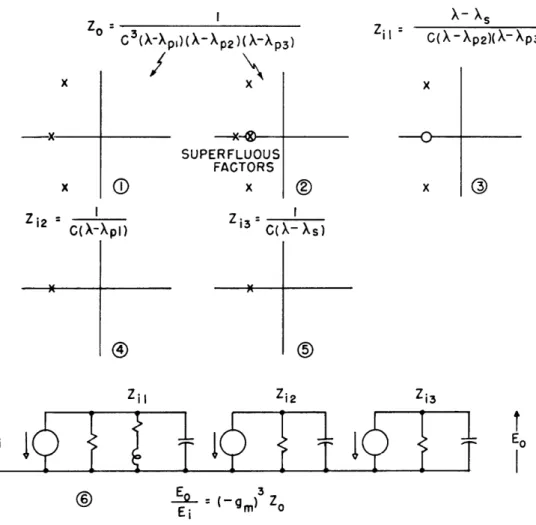
Zo = Zil Zi2 x ... Zin (24)
Each interstage impedance must approach 1/XC as X + c; hence, the Zi's must each have one more pole than zeros. In considering Zo, one appreciates that the adding of surplus factors in the numerator and denominator is entirely appropriate, since the value of ZO is unchanged by this process. With addition of factors, Eq. 5 is of the form
-1 (Xk- Xks) (X - Xs2) ... (X - Xsq)
Z . (5')
C
cn( - Xpl) (- p2)... (- pn) (- Xsl ) (-- s2)... ( -- xsq)
That all of the surplus poles and zeros should be on the negative real axis for the network realization presented is seen presently as the method of choosing the superfluous factors is described. Accordingly the map of poles and zeros in the complex plane is indicated in Fig. 14.
At this point one should consider the simplest functions which could be associated with the Zi's, bearing in mind that the function must have one more pole than zeros; in particular, must approach /XC as X o. The first case is a function with only one pole on the negative real axis of the X-plane, as illustrated in Fig. 15. This case leads to the RC network shown, the element values of which are related to the pole position, as shown in the figure. One observes that there is no restriction on the position of the pole in Fig. 15 other than that it be on the negative real axis. In general, the position merely determines the size of R, the nearer the pole to the origin the smaller the value of R. The next case is that in which Zi has a conjugate pair of poles. Then it must
have a single zero on the negative real axis. For such a function to be positive real,
I
c Zll 2 aIpl
I,
which means that the zero associated with a pair of poles in such an interstage impedance can lie anywhere in the region indicated in Fig. 16. The validity of this condition of positive real character is verified by considering the reciprocal of Zi for Fig. 16. The consideration of that quantity also identifies the network realization.1 _ C(X - pl -
ijpl)
(X - -pl + jipl)Zi 1 X zl
C(k22pl X pl + P) +
p1 Xa zl
For the real part of 1/Z i is to be positive as X = jm- jo, zl - aZpl must be greater
than zero, and the condition
o
zl 1< 2 la pl I is proved necessary. The condition is sufficient, since it leads to the possibility of identification of the network of Fig. 17 with Zi. An examination of Fig. 17 reveals that the position of o' zl i n the range of possiblevalues regulates the sizes of R and RL. If zl = 2 p R = and is accordingly absent. If zl = 0, RL = 0 and is absent. Any value of C zl between zero and 2a pl corresponds to a network in which R and RL, both with finite values, are required.
The preceding discussion has shown two kinds of simple networks suitable to be identified with factors of Zo, as shown in Eq. 24. The choice of superfluous factors as indicated in Eq. 5' and the subsequent network realization will now be outlined.
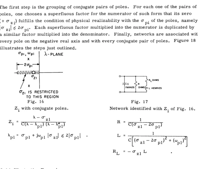
The first step is the grouping of conjugate pairs of poles. For each one of the pairs of poles, one chooses a superfluous factor for the numerator of such form that its zero (+ - zi ) fulfills the condition of physical realizability with the a pi of the poles, namely Ir Zil Zrpi' Each superfluous factor multiplied into the numerator is duplicated by
a similar factor multiplied into the denominator. Finally, networks are associated with every pole on the negative real axis and with every conjugate pair of poles. Figure 18
illustrates the steps just outlined. PI, PI X- PLANE
X
h-
2p lRLOHMS
FARADS OHMS L HENRIES
,'zi IS RESTRICTED TO THIS REGION
Fig. 16 Fig. 17
Zi with conjugate poles. Network identified with Zi of Fig. 16.
X-(r zl Z. R = 1i C(k- Xpl ) (X -
-
l) = C( C(O-zl 2a p ) R = kpl = -pl + JWpl la7zlJ < 216pl . RL =- Czl L 2.14 Illustrative ExampleThe design of a five-stage low-pass amplifier using 6AC7's and having a cut-off frequency of 16.5 megacycles is illustrated. In the design, which uses two-terminal interstages, a Tschebyscheff characteristic will be applied, giving 10 percent vari-ations of amplification in the pass band. As indicated earlier, such a design gives an amplification which is 24 percent of the theoretical limit imposed by parasitic capacitance, or 0.24 (gm2/Co)5 , which is (using 9000 mhos as gm and 25 p~Lf as C) 3920. Figure
19 shows a sketch of the amplification characteristic of the design. In the design, it is convenient to work first with a 1 rad/sec case. The C's here are 25 x 10 1 2 x 16.5 x 106 x 2r, or 2.59 x 10 3 farads. The design will be transformed later to the 16.5-megacycle basis by diminishing the size of all inductances and capacitances. The poles of ZO for the 1 rad/sec case are found through Eq. 21 and are located at - 0. 300, - 0. 243 + j 0. 614, and - 0. 093 + j 0. 994, as shown in Fig. 20. For the present example, Z is
(for 1 rad/sec case)
1
2.59 x 10 (X + 0. 300) (Xk + 0.486k + 0.243 + 0. 614) kX + 0. 186k +(0. 093)2+ 0. 9942 (26)
Zil 3(X-Xpl) (X-Xp2)(X-Xp3)
/
X SUPERFLUOUS FACTORS x Zi C(- s) Zi2 X- Xs c(X -XP2)( X- XP3) X -0--O xQ
Zi3T
1
Y
I
T
() EO = (-gm) Zo E iFig. 18 Illustration of network Zo = Zil Zi Zi3'
realization of Z of form of Eq. 5.
XI X |AMP 3920… 0 _______________ 165MC f -x jlX- PLANE x - POLES -jl Fig. 19 Characteristic of five-stage, 16. 5-Mc amplifier. Fig. 20
Position of poles for illustrative example. -18-zo
f
x
X Zi2 = C(X-pl) Zil * ,It
EiI
-- I- _ .-v . . ... . >6AC7 TUBES gm = 9000 1LLmhos
Fig. 21 Network for five-stage amplifier.
L 1 (henries) L2 1 rad/sec model 2.59 x 10 1287.0 1589.0 249.0 4150.0 36.5 1025.0 391.0 16.5 x 10⁶ cps model 25.0 x 10 1287.0 1589.0 249.0 4150.0 36.5 9.89 x 10⁶ 3.75 x 10- 6
FOR BOTH CIRCUITS E F(X)
El O- O BAND PASS JX k ( .'+ WC ._,· k \ae C- W) LOW PASS jx X j (W) FOR LOW PASS CASE S A C
~~~~~~~~~~~~~~I
X(W) FOR BAND PASS CASE |Eo IEl X -UCFig. 23 Illustration of principle of con-servation of bandwidth. E /E = F(X). Left, low-pass case, jX = j
Right, band-pass case, jX = j-jo2c//.
WaC
NETWORK CONFIGURATION IS THE SAME FOR BOTH CIRCUITS IN THE SENSE THAT EVERY
IN THE LOW PASS CASE [ °--o
L HENRIES IS REPLACED BY kL h I f
Wc kwcL
IN THE LOW PASS CASE o-AI - o
C FARADS IS REPLACED BY
I/k acCh
I
t
Fig. 22 Summary of low pass-band pass transformation.
Fig. 24 Band-pass network corres-ponding to Fig. 18.
-19-t
R Ei V0 R 'f IR L 0 G L I I Element C(farads) R1 (ohms) - - --- --- - ---- ·--- --· v I )which is split into factors (using appropriate superfluous factors) giving 1 X + 0.243 2.59 x 10 3 (X + 0.300) 2.59 x 10- (x2 + 0.486X + 0.2432 + 0.6142) 1 x + 0. 093 2. 59 x 10 ( + 0. 243) 2.59 x 10³ (X + 0. 186 + 0.093 + 0. 994 1 AV -3 (27) 2.59 x 10 (X+ 0.093)
According to the results of Fig. 16 and Fig. 17, this factoring leads to the equivalent circuit of Fig. 21 with the table of element values shown.
2. 15 Extension of Design Method Presented to More General Specifications
The preceding development and examples have illustrated a compact design procedure for low-pass amplifiers consisting of one chain with two-terminal interstages. Such a design involving Tschebyscheff polynomials is very convenient and involves minor effort on the part of the designer. It is illuminating, in that one recognizes easily how effec-tively the resulting amplifier approaches the limit set by parasitic capacitance and the tolerance on uniformity in the pass band can be set in the beginning. The solution to the approximation problem is direct and explicit. The network so designed always has a low-pass characteristic and a set form of phase characteristic accompanying the
choice of magnitude characteristic made. In the design process one does not directly govern the phase characteristic, but does this implicitly when he specifies the magnitude
characteristic. The question to be raised at this point is: How can one design amplifiers with specifications on the characteristics which are more general than those of the
low-pass amplifiers just discussed (an amplifier with band-low-pass characteristics or specified phase characteristics, for example)? In answering the question, two different
pro-cedures will be discussed. The first procedure applies long-established methods of transformation to yield networks with band-pass characteristics from a corresponding network with low-pass characteristics. This method turns out to be rather special and limited. The second procedure involves the use of the characteristics of a low-pass design as presented to be a very rough guide from which one proceeds to designs having
much more complicated specifications to meet.
2.16 The Conventional Low-Pass to Band-Pass Transformation
In order to adapt a given low-pass design to a band-pass design, a method widely used is the replacing of every capacitance by a parallel-tuned circuit, and every induc-tance by a series-tuned circuit. Every tuned circuit is resonant at c which is the geo-metric center of the pass band (14). The low-pass to band-pass transformation is really a frequency-variable transformation applied to the system function. Every X in the low-pass function is replaced by k (X/wcc + wc/X) to obtain the band-low-pass function. One recalls that a system function is always equivalent to the ratio of determinants in which typical
elements or components of elements are of the nature Lk or 1/Ck. The variable trans-formation applied to the elements of the determinants replace Lk by L k X/c + L k c/ and 1/CX by
1 Cko
CkX + c
c
which are, respectively, the impedance of a series-tuned circuit and the impedance of a parallel-tuned circuit. The transformation represents a shift of the characteristics of the low-pass circuit to higher frequencies. Figure 22 shows the relationship between the behavior of the circuits and their elements. If k is equal to c', the result is that every capacitance is replaced by the same capacitance in parallel with an inductance. Moreover, the behavior of such low-pass and band-pass circuits has an interesting
feature called the conservation of bandwidth, which is illustrated in Fig. 23. The reason for the behavior illustrated in Fig. 23 is quite simple. IEo/Eil is an even function of X. For the band-pass case if wa leads to Xa,
2 2 o co X = -- ; then =-.leads to -X . (28) a a oa a a a a 2 2 co oa - o = X or o -- o a = _ x a . (29) a
But the difference between the frequencies leading to Xa and-X a is a - w2/a' which
is X a
This case is an example of the fact that parasitic capacitance imposes the same restriction on bandwidth regardless of the position of the band in the spectrum.
To illustrate a network using the low-pass to band-pass transformation, Fig. 24 is shown. It represents the band-pass network corresponding to Fig. 18.
2.17 An Alternate View of the Low-Pass to Band-Pass Transformation
The discussion just completed illustrates the obtaining of band-pass networks from low-pass networks. The generality of the method is limited to this one problem. A second procedure will be introduced at this point which permits more general variations. It is introduced through consideration of the same low-pass to band-pass transformation considered from a different point of view. The discussion concerning the low-pass to band-pass transformation has been conducted, up to this point, in terms of the changes
made in the network to get a band-pass from a low-pass network. The consideration of a shift in poles and zeros of the amplification function brought about by the same transformation is very illuminating. That poles and zeros of amplification occur for
similar values of X for both the low-pass and the band-pass designs is clear from Fig. 22. For example, if for Xz there is a zero of the amplification function, then in the low-pass design there is a zero at
X = jXz + . (30) In the corresponding band-pass design (for which the frequency variable will be denoted by primed quantities) a zero will occur at the place where
2 F X 'c X,+ ' (31) Equation 31 is equivalent to : 2 2 X' 2 _(a- + j ) + 02 0 (32)
Zeros for the band-pass case are at
Oz z + jZ) 2
z_ -+ z
4
2 c (33)The last expression indicates that if wc is large in comparison to z and z, in the band-pass case critical frequencies will be distributed around + jic with half the displacement of the corresponding critical frequencies from = 0 in the low-pass case. If a- and
z
oz are not small compared to x c, the critical frequencies are displaced from (0 + j z)2_
+ z z)
4 c
In addition to the internal critical frequencies covered by Eq. 33, it is clear that for
any poles or zeros at zero in the low-pass case there will be poles or zeros at + JWc
in the band-pass case. For any poles or zeros at infinity in the low-pass case there
will be corresponding poles at both zero and infinity in the band-pass case. Figure 25
x
x
LOW- PASS MAP
A- PLANL
3 ZEROS AT co
(1
-_
__--Fig. 25 Critical frequency maps for corresponding low and band-pass amplification functions.
illustrates the shift occurring in critical frequencies for a low-pass to band-pass transformation. Figure 25 and Eq. 33 indicate that if poles were placed on a semi-ellipse centered at zero in the low-pass case, corresponding poles are placed on a
semi-ellipse centered at c in the band-pass case if c is sufficiently large. If, on the
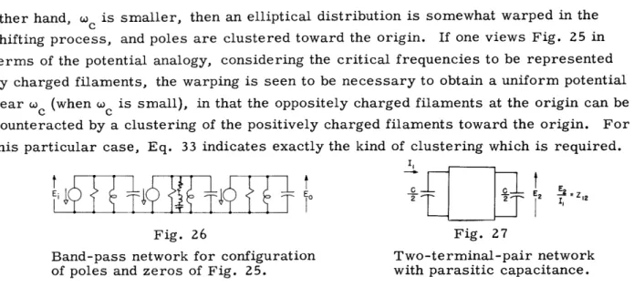
-22-other hand, w0 is smaller, then an elliptical distribution is somewhat warped in the shifting process, and poles are clustered toward the origin. If one views Fig. 25 in terms of the potential analogy, considering the critical frequencies to be represented by charged filaments, the warping is seen to be necessary to obtain a uniform potential near wc (when wc is small), in that the oppositely charged filaments at the origin can be
counteracted by a clustering of the positively charged filaments toward the origin. For this particular case, Eq. 33 indicates exactly the kind of clustering which is required.
(E, ( < tX2 7 E 5,
Fig. 26 Fig. 27
Band-pass network for configuration Two-terminal-pair network of poles and zeros of Fig. 25. with parasitic capacitance. An interesting result of the consideration of the pole and zero shifting procedure for the low-pass to band-pass transformation is the fact that a band-pass network corresponding to Fig. 25 is that of Fig. 26. This is arrived at by simply considering Fig. 17. The circuit of Fig. 26 is exactly the equivalent of that of Fig. 24 and is
somewhat simpler. The reason for the simplicity in this case is that the transformation has placed the right number of zeros at the origin, and the network realization can be carried out without the adding of superfluous factors as was necessaryin Fig. 18. The low-pass to band-pass transformation done in terms of the network (as in Fig. 24) frequently leads to a more complicated network.
From the foregoing it is clear that the design of low-pass or band-pass amplifiers with Tschebyscheff behavior of the magnitude of amplification in the pass band is con-veniently carried out through the use of Tschebyscheff polynomials to give an explicit solution. The preceding discussion has indicated that parasitic capacitance imposes the same limitation on amplification regardless of value of the center frequency of the band.
The design method just discussed is satisfactory as a final answer in a small fraction of amplifier design problems. Two examples follow, illustrating cases wherein the method discussed does not give a final answer.
If the coils used in an amplifier are appreciably lossy, the equivalent circuit of Fig. 26 cannot accurately represent the circuit. If the circuit required by the design needs lossless coils, and practical coils with loss are used in the physical circuit, then it is impossible to realize zeros of amplification at zero as indicated in Fig. 25. One would like to find an alternate solution to the approximation problem giving about the same amplification characteristics but not requiring zeros on the imaginary axis. The solution to the approximation problem, using Tschebyscheff polynomials, is fairly close to what is required but is not exactly what is needed. A practical solution to the problem is to place the zeros of amplification (Fig. 25) in the left half-plane and then
to shift the poles slightly to compensate for any bad effect resulting in the characteristic
arising from the zero shift. In this case the Tschebyscheff approximation has served as a first estimate, and the solution is subsequently fitted to the practical conditions. The technique of shifting pole and zero positions to achieve desired changes in the amplification function character is treated in the companion report (11). Through the use of this technique, a very wide variety of problems can be solved in which design conditions are accommodated which would be impossible in other approximation methods.
A second illustrative example in which the explicit approximation procedure using Tschebyscheff polynomials is unsatisfactory is a case in which a band-pass amplifier with approximately linear phase shift in the pass band is desired. The phase character-istics accompanying Tschebyscheff behavior of the magnitude are notably nonlinear. However, one can start with the pole and zero positions from a Tschebyscheff
approxi-mation, and make appropriate shifts of the poles and zeros to accomplish the desired changes in the phase characteristic. The procedure for this adjustment process is given in the companion report (11).
This section has presented to this point a rather complete account of the design of amplifier chains with two-terminal interstages. The limitation imposed by parasitic capacitance is very definite. It has been pointed out that the most convenient quantities through which to define network behavior and to solve the approximation problem are the pole and zero positions of the amplification function of the chain. Network reali-zations have been presented in which network configuration and element values are specified in terms of the pole and zero positions of the amplification function. The use of Tschebyscheff polynomials in obtaining low- or band-pass designs has been discussed. An introduction has been made of the method of altering a given first trial using such an approximation as a first estimate, to be followed by better approximations to the desired characteristics. The method described is applicable in the design of amplifiers composed of a single chain, or of amplifiers comprising several chains which are paralleled at the load. As will be seen later, the essence of a successful design pro-cedure for a multi-chain amplifier is the ability to control the characteristics of the individual chains, thereby shaping them to fit each other in an effective manner. 2.20 Two-Terminal-Pair Interstages
The results developed and stated to this point in the present section all apply to amplifiers with two-terminal interstages. The remainder of the section is devoted to two-terminal-pair interstages. First, the limitation imposed by parasitic capacitance
on the amplification bandwidth product is discussed. Unfortunately, the evaluation and interpretation of the limitation is much more difficult for the two-terminal-pair case than it is for the two-terminal case, and the results cannot be expressed in definite,
conclusive form for the most general situations. However, the information available does provide a useful guide in the design of amplifiers with two-terminal-pair interstages. The significant point is that the limitation on amplification imposed by parasitic capa-citance is lessened if the parasitic capacapa-citance can be split into two parts by a coupling
network. It is difficult to put a limit on the advantage which is gained by splitting. A set of simple, practical, double-tuned circuits are considered. Their configuration and element values are associated with the position of poles and zeros of transfer impedances in a manner consistent with the treatment of the two-terminal case already discussed. The presentation, as a whole, is made to facilitate the application of the approximation procedure developed in R.L.E. Report No. 145.
2. 21 Limitation Imposed by Parasitic Capacitance for Two-Terminal-Pair Interstages The amplification of a chain of n amplifiers is
E
(
g )n zzz
(1)E. i ( - gm) Zil Zi"Z .... (1)
When the amplifiers are connected by two-terminal-pair interstages, the Zi's of Eq. 1 are transfer impedances. Accordingly, the logical question to ask in connection with Eq. 1 is: What limitation is imposed on the uniform level of magnitude of Zil Zi.... Zin by the fact that parasitic capacitance shunts both the input and output terminals of each interstage? An exact answer is not available for a product of impedances. Bode has answered the question for a single interstage. His solution will be discussed at this point.
2.22 Bode's Result (15)
The maximum constant level of transfer impedance over w0 rad/sec of a passive two-terminal-pair network is wr2/2Cwo ohms. C is the sum of equal shunt capacitances at the terminals of the network (Fig. 27). Further, the network which attains the limit must be symmetrical. Though no comprehensive study will be made here of Bode's attack on the problem, it is helpful to indicate wherein the limitation arises, to better define its nature.
Gewertz has shown the necessary and sufficient conditions of physical realizability for two-terminal-pair networks. Bode applies these results in the form which states that for any real frequency (X = j) the product of real components of open-circuit
imped-ances from the two-terminal pairs is greater than, or at least equal to, the square of the real part of the transfer impedance. These quantities are indicated in Fig. 28. The
condition mentioned indicates that if there is a limit on the driving-point impedances, then there is implicitly a limit on the transfer impedance. The parasitic capacitances
do impose a limit on the impedances ZA and ZB. This limit is in the form of the
resistance integral theorem (16), which is:
o RA d oRB do0 w = (34)
0 0
It is improper to assign a level of ZA or ZB so high that Eq. 34 cannot be satisfied for the capacitance present. But the level of magnitude of Z 12 is implicitly limited by the
_I :l L
-p_
In realizable networks
E E / E 2
ReA Re >
Fig. 28 Gewertz's condition of physical realizability by Bode.
t
(a) I 3 E" I (b) Fig. 29 Circuit providing maximum uniformZ 12 1 over o0 rad/sec
II ---I
(a) (b)
Fig. 30 Circuit fullfilling relation 36 with equality sign.
2
4 C1 C2 o
Co
Fig. 31 Multi-terminal-pair net-work with parasitic capacitance.
I:1
Fig. 32 Two terminal-pair network constructed from the network of Fig. 31.
-26-IA EA B