HAL Id: hal-01838614
https://hal.laas.fr/hal-01838614
Submitted on 13 Jul 2018
HAL is a multi-disciplinary open access
archive for the deposit and dissemination of
sci-entific research documents, whether they are
pub-lished or not. The documents may come from
teaching and research institutions in France or
abroad, or from public or private research centers.
L’archive ouverte pluridisciplinaire HAL, est
destinée au dépôt et à la diffusion de documents
scientifiques de niveau recherche, publiés ou non,
émanant des établissements d’enseignement et de
recherche français ou étrangers, des laboratoires
publics ou privés.
Passive and Chipless Packaged Transducer for Wireless
Pressure Measurement
Julien Philippe, Maria Valeria de Paolis, Cristina Arenas-Buendia, Dominique
Henry, Anthony Coustou, Alexandre Rumeau, Hervé Aubert, Patrick Pons
To cite this version:
Julien Philippe, Maria Valeria de Paolis, Cristina Arenas-Buendia, Dominique Henry, Anthony
Cous-tou, et al.. Passive and Chipless Packaged Transducer for Wireless Pressure Measurement. Sensors and
Actuators A: Physical , Elsevier, 2018, 279, pp.753-762. �10.1016/j.sna.2018.06.024�. �hal-01838614�
Passive and Chipless Packaged Transducer for Wireless
Pressure Measurement
J. Philippe, M.V. De Paolis, C. Arenas-Buendia, D. Henry, A. Coustou, A. Rumeau, H. Aubert, P. Pons
LAAS-CNRS, Université de Toulouse, CNRS, INP, Toulouse, France 7, Avenue du Colonel Roche – BP54200
31031 TOULOUSE cedex 4 - FRANCE Correspondence: [email protected]
Abstract: A new microwave fully passive, chipless and packaged sensor for wireless pressure
monitoring in harsh environments (such as, extreme temperature, radioactive and/or toxic environments) is proposed in this paper. The sensor consists of a planar microstrip resonator, which is electromagnetically coupled with a high resistivity and thin silicon membrane. Prototypes have been designed and fabricated using a photoresist intermediate layer for the silicon membrane bonding. The electromagnetic simulation of the system is also performed in order to predict the transducer performances. Measurement results using the packaged sensor are provided to experimentally validate the simulation results and the manufacturing process.
Keywords: Passive sensor; chipless sensor; pressure sensor 1. Introduction
Wireless, batteryless (no power supply) and chipless (no electronic circuit) sensors are a promising solution for remote measurements of physical quantities in high radiation or extreme temperature environments, or/and when the battery replacement is difficult or induces high costs. Such remote measurements require two main units: (1) the sensing unit, which is sensitive to any variation of the (physical or chemical) quantity of interest, and (2) the reader, which allows wireless interrogation of the sensing unit. Electromagnetic (EM) sensors operating in the microwave frequency range (see, e.g., [1-3]) are advantageously used here in the sensing unit while a Frequency-Modulated Continuous-Wave (FMCW) radar will serve in our future work as the reader (see, e.g., [4]). A reading range up to 58 meters of passive humidity EM sensors using such a radar was recently reported in [5].
Literature reports many developments performed on passive pressure sensors with different technologies and devices, such as, e.g., microwave circuits [6] [7], microwave cavity resonators [8], evanescent mode resonator [9], slot antenna integrated resonator [10], capacitive sensors [11], or dielectric resonators [12]. Table I reports some of their characteristics in terms of pressure measurement range, operating frequency fres, full-scale frequency range, and the measurement sensitivity.
Table I. Wireless, passive, and chipless pressure sensors reported in the Literature. Reference Pressure range fres (GHz) full-scale frequency range
(absolute // relative) Measurement Sensitivity [10] 0.4 – 1.2 bar 2.107 6 MHz // 0.28% 7.31 MHz / bar [8] 0 - 736 Pa 5.16 50 MHz // 0.97% 16 MHz / Pa [7] 1 – 1.8 bar 9.61 25 MHz // 0.26% 0.16 MHz / bar [9] 0 – 5.3 bar 11.75 200 MHz // 1.7% 35 MHz / bar [11] 0 – 900 Pa 15 16 MHz // 0.11% 0.22 MHz / Pa [12] 0 – 4 bar 20.53 2.2 GHz // 11% 455 MHz / bar [6] 0 – 3 bar 39 1.1 GHz // 2.8% 370 MHz / bar
In view of this state of the art as it will be shown in this paper, our packaged pressure sensor offers a larger absolute full-scale frequency range and higher measurement sensitivity.
This paper deals with the manufacturing of passive and wireless microwave sensors for pressure monitoring. These sensors are based on two transductions: (1) the mechanical transduction, which converts the pressure variation into the deflection of a thin membrane, and (2) the electromagnetic
transduction, which converts this deflection into the variation of the scattering parameters of the
microwave resonator. As an application, pressure monitoring in nuclear plant buildings is targeted. The first part of the paper reports the design and the technological manufacturing process of the proposed pressure sensor. Next, mechanical and full-wave electromagnetic simulation results are discussed and last but not least, the predicted sensor performances in terms of full-scale range and sensitivity are experimentally validated.
2. Working principle and design of the EM pressure sensor
The passive pressure sensor is a planar microwave resonator, which is electromagnetically coupled with a high resistivity thin silicon (Si) membrane. In the previous design and first concept reported in [6], the coplanar (CPW) technology was applied for fabricating the microwave resonator (Fig. 1). However, the packaging of this solution required input and output CPW-to-microstrip discontinuities (see Fig. 2) which may excite multiple undesirable spurious modes in addition to the resonant frequency of the resonator.
As shown in Fig. 3, the use of the microstrip technology instead of a CPW technology allows us the removal of eventual spurious resonances. A high-resistivity Si membrane is placed above the resonator located inside a cavity (Fig. 4). All the dimensions of the structure are reported in Figs. 4 and 5.
Fig. 1. Top (top) and
bottom (bottom) views of the CPW microwave resonator with its thin membrane [6].
Fig. 2. View of the
microstrip-to-CPW transition inside the packaging (bottom) and with the packaging cover (top).
Fig. 3. Measured transmission coefficient (S12)
versus frequency of a packaged microstrip line (in blue) and of a packaged CPW line with its input and output microstrip-to-CPW discontinuities (in orange).
Fig. 4. Cross-sectional view of the different sensor layers.
The resistivity (ρ), the relative permittivity (εr), and the
loss tangent (tan δ) of each material are also given.
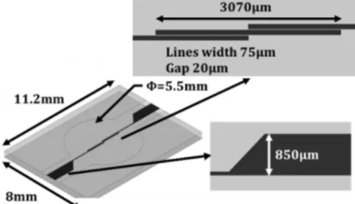
Fig. 5. Dimensions of the microstrip resonator. Φ denotes
3. Manufacturing process
The manufacturing process is described in Fig. 6. It uses a 500 µm thick borosilicate glass (B33) substrate. After piranha and plasma cleaning, a 0.55 µm thick chromium-aluminum (Cr-Al) layer allows manufacturing of the planar microwave resonator by using PVD deposition and lift-off patterning. The ground plane is fabricated by PVD deposition of a 1.55 µm thick Cr-Al layer. A high resistivity Si (100) membrane of thickness 100 µm ± 10 µm is then bonded over the resonator using a low-loss photoresist (thickness of 16 µm). This bonding solution provides a quite simple process to guarantee the sensor is sufficiently hermetic.
Fig. 6. Description of the manufacturing process of the microwave sensor.
4. Manufacturing analysis
4.1. Thicknesses measurement
Resonator metallization and cavity thicknesses were measured before and after the bonding in order to (1) predict the sensor performances and (2) check the reliability of the manufacturing process.
4.1.1. Measured thicknesses before the bonding
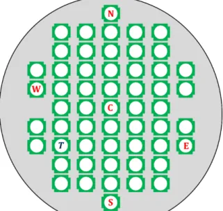
In Fig. 7, the locations of the thickness measurement are indicated with the letters C (center), E (east), N (north), S (south) and W (west). Table II gives the thicknesses measured from a mechanical profilometer with an accuracy of ±0.1 µm for the photoresist and of ±0.01 µm for the metallization of the resonator. It is found that the resonator metallization and photoresist layer are deposited at an average acceptable thickness of respectively 0.57 µm and 15.7 µm with an average deviation of ±0.02 µm (3.5 %) and ±0.5 µm (3.2 %). Si membranes thicknesses were also measured using a dial test indicator with an accuracy of ±1 µm. For a given membrane, measurements indicate that the thickness ranges between 102 µm and 105 µm.
Table II. Measured thicknesses of the resonator metallization and photoresist layer (in µm). Center C North N East E South S West W Average deviation Average
Photoresist 16.5 15.9 15.6 15.9 14.8 15.7 0.45
Resonator
4.1.2. Measured thicknesses after the bonding
After the bonding step, the separation distance between the bottom of the Si membrane and the planar resonator was measured by using X-ray microtomography at different points on the circular cavity. The measurement resolution is of 2.5 - 3 µm and the measurement accuracy is of ±0.1 µm. The variation from the center point of the cavity thickness is between -1.7 % and 5.1 % (see Fig. 8). The separation distance between the planar resonator and the bottom of the membrane is then quasi-uniform inside the circular cavity. The cavity thickness of the sensor (placed at point T in Fig. 7) was also measured using interferometric profilometry technique with a measurement accuracy of ± 0.5 µm. This distance is evaluated at 15.2 µm ± 0.5 µm. In the next section, both airtightness and resilience to pressure hysteresis of the sensors will be evaluated in order to validate the technological process and materials choice.
Fig. 7. Map of the different cells on the substrate. Green
patterns represent the different cavities. C, E, N, S, T, W denote Center, East, North, South, Transducer, and West, respectively.
Fig. 8. Upper (top) and cross-sectional (bottom)
micrograph for X-ray microtomography thickness measurement.
4.2. Airtightness measurement
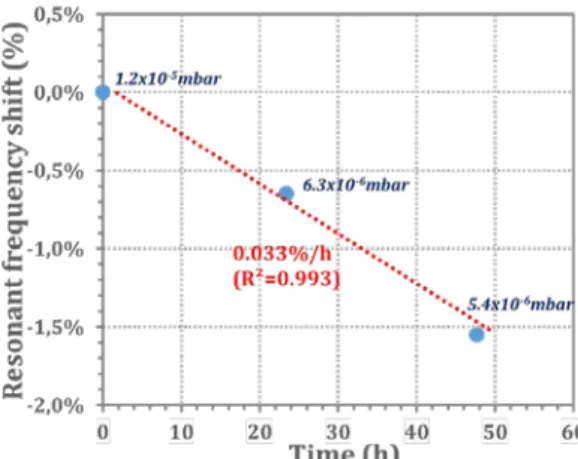
To check the structure is hermetic, the sensors were placed inside a chamber where the vacuum was maintained for some days. The resonant frequency of the planar resonator was measured with a Vectorial Network Analyzer (VNA), as it will be detailed in Section 6. The results are displayed in Fig. 9. From the frequency measured when vacuum is established (1.2x10⁻⁵ mbar), it is observed that the
circular cavity is not fully hermetic: an undesirable decrease of 7.54 MHz per hour (or equivalently of 0.035 % per hour) of the resonant frequency occurs. However, as a pressure monitoring will be performed in less than one hour in our application, it can be concluded that the sensors’ airtightness sufficient to demonstrate the proof-of-concept.
4.3. Resilience to pressure hysteresis of the fabricated sensors
The samples were placed inside a hermetic chamber. The resilience to pressure hysteresis was measured by applying pressure cycles {atmosphere pressure – vacuum} and by measuring the resulting resonant frequency shift after the air filling of the chamber. The measurement results are reported in Table III. In the worst case, the resonant frequency changes from the initial value fref of ± 0.90 % (± 205 MHz for fref = 22.8 GHz). The resilience to pressure hysteresis of the sensors is therefore acceptable for the proof-of-concept phase.
Table III. Resonant frequency variation after pressure cycles.
Cycle number Cycle 0 Cycle 1 Cycle 2
Resonant frequency (%) – cell 1 fref fref .(1 – 0.43%) fref .(1 – 0.90%)
Resonant frequency (%) – cell 2 fref fref .(1 + 0.17%) fref .(1 – 0.35%)
5. Full-wave electromagnetic simulation of the pressure sensor
The performances in terms of full-scale range and sensitivity of the microwave pressure sensor were evaluated by using rigorous (full-wave) electromagnetic simulations. These simulations were performed by using ANSYS HFSS commercial software [13].
5.1. Simulated sensor performances without overpressure
Considering the transducer described in Figs. 4 and 5, the effect of the cavity thickness on the electromagnetic descriptors is first studied. The cavity and membrane thicknesses of the transducer (placed at point T in Fig. 7) are respectively of 15.2 µm ± 0.5 µm and between 102 µm and 105 µm. From electromagnetic simulations, the resulting resonant frequency of the planar resonator is expected between 22.6 GHz and 22.8 GHz for a Si membrane thickness of 105 µm (see Table IV).
Table IV. Simulation of the cavity thickness impact on the resonant frequency for a Si membrane
thickness of 105µm.
Cavity thickness (µm) 14 15 16
Resonant frequency (GHz) 22.60 22.75 22.80
Table V. Simulation of the silicon thickness impact on the resonant frequency for a cavity thickness of
16µm.
Cavity thickness (µm) 100 102 105
Resonant frequency (GHz) 22.88 22.83 22.80
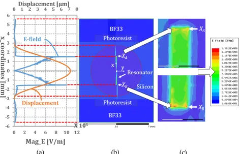
The very small non-uniformity (5µm) of the membrane thickness is expected to generate a acceptable frequency shift of 80 MHz (~0.35 %) of the resonant frequency (see Table V). The amplitude of the microwave electric field (E-field) on the microwave resonator surface was also computed. As observed from Fig. 10 (a) and (c), the maximum E-field amplitude is located at the two edges of the half-wavelength microstrip resonator (coordinates XA = 1.535 mm and XB = -1.535 mm in Fig. 10). The E-field
amplitude decreases abruptly by moving away from the edges (see Fig. 10 (c)).
(a) (b) (c)
Fig. 10. a) Amplitude of the microwave electric field (blue line) at the resonant frequency of 22.85 GHz along the
x-axis and the corresponding displacement (orange line) along this axis when the overpressure of 1 bar is applied; (b) the 2D E-field distribution on the microwave resonator surface at the atmospheric pressure; c) zoom of the electric field amplitude at coordinates XA and XB.
5.2 Simulated sensor performances with overpressure
In order to analyze the performances of the sensor when the overpressure occurs on the Si membrane, it is necessary to compute the membrane deflection when a pressure is applied. An accurate model for membrane deformation prediction is now described.
5.2.1 Mechanical modelling
The deflection of the membrane when the pressure is applied (that is, when a gradient is created between pressures inside and outside of the cavity) can be simulated from a close-form expression and from rigorous simulation techniques.
When the pressure is applied on the Si membrane surface, the resulting membrane deflection can be derived from a fourth-order differential equation. The solutions of this equation depend on the geometry (square, circular, rectangular, etc.), dimensions, and mechanical properties of the membrane [14]. As the cavity is circular in our case, only membranes with circular geometry were considered here. The deflection 𝑊𝑊(𝑟𝑟) of the membrane when an overpressure is applied on its surface can be approximated by the following close-form expression (see Fig. 11) [15]:
𝑊𝑊(𝑟𝑟) = 𝑊𝑊0𝑊𝑊𝑁𝑁 (𝑟𝑟) (1)
where W0 denotes the maximum deflection at the membrane center, and WN(r) designates the distance from the center. For the circular membrane, W0 and WN(r) can be approximated as follows [15]:
𝑊𝑊0= 12𝑅𝑅 4(1−𝜈𝜈2) 64𝐸𝐸𝑒𝑒3 𝑃𝑃 (2) 𝑊𝑊𝑁𝑁 (𝑟𝑟) = (1 −𝑟𝑟 2 𝑅𝑅2)2 (3)
where R and e denote respectively the radius and the (uniform) thickness of the membrane while E, ν, and P are respectively the Young’s modulus, the Poisson’s ratio, and the applied overpressure.
From Eq. (1), it can be observed that the deflection depends only on dimensions ( R and e) and mechanical properties (E and ν) of the circular membrane.
Fig. 11. Membrane geometry (left) and deflection 𝑊𝑊(𝑟𝑟) when an overpressure P is applied on its surface (right).
mechanical properties (E and ν) of the circular membrane. For a membrane radius R of 2750 µm and a thickness e of 105 µm, and assuming that the direction of the Si membrane deflection occurs along the crystallographic direction <001>, we will set E to 130 GPa and ν to 0.28. Moreover, in our application, the applied overpressure P will vary between 0 to 2.5 bars. The membrane deflection when the pressure is applied was also analyzed from rigorous mechanical simulations by using COMSOL Multiphysics commercial software [16]. These simulations allow taking into account the geometry and mechanical properties of the constitutive materials (Si, photoresist, and B33 materials) of the sensor. Assuming that the Si membrane deflection occurs in the crystallographic direction <001>, a so-called pressure boundary load was assigned along the z-axis to the top faces B33, Si, and photoresist materials (see Fig. 12 (a)), while the fixed constraint (perfect clamping) was assumed on the bottom side of the B33 material, as illustrated in Fig. 12 (b). Fig. 13 shows the simulated total deformation of the membrane obtained from COMSOL Multiphysics software by assuming an applied overpressure of 1 bar, and Fig. 14 displays the maximal membrane deflection as a function of the applied overpressure. As expected, a linear relationship is obtained both from the close-form expression of Eq.(1) and from the rigorous mechanical simulations. Moreover, the difference between the results given by these two simulation approaches does not exceed 9%. From these results, the pressure beyond which the membrane is in contact with the planar resonator can be predicted. From the close-form expression, this pressure is of 2.44 bars (see point
P1 in Fig. 14(a)) while the rigorous membrane simulation gives 2.23 bars (see point P2 in Fig. 14(a)).
(a)
(b)
Fig. 12. The two structural mechanical boundary conditions: a) a pressure boundary load was assigned along
the z-axis and on the top side of the B33, Si and photoresist materials (in purple); b) a fixed constraint (perfect clamping) was assumed on the bottom side of the B33 material (hatched region). It was assumed to model a sensor with a 16 µm thick cavity and a 105 µm thick silicon membrane.
Fig. 13. Simulated total displacement [µm] for an applied overpressure of 1 bar. The mechanical simulations
(a)
(b)
Fig. 14. Membrane deflection as a function of the applied overpressure P obtained from the close-form
expression of Eq.(1) and from COMSOL Multiphysics simulations [16]: a) displacement [µm] versus the applied overpressure [bar] at the center of the circular membrane ; b) displacement [µm] along the x-axis of the Si membrane for an applied overpressure of 1 bar. It was assumed to model a sensor having with a 16 µm thick cavity and a 105 µm thick silicon membrane.
5.2.2 Electromagnetic simulation of the microwave pressure sensor
In order to analyze the impact of the membrane deflection on the performance of the microwave pressure sensor, rigorous (full-wave) electromagnetic simulations were performed by using of ANSYS HFSS commercial software [13] and by applying a flat membrane model (the clamping condition of the membrane is then taken into account in these simulations). The electromagnetic simulations were performed for the displacements d extracted from the following simulation conditions:
• Case A: where the electrical field E-field is maximum, i.e. in x = XA for the corresponding
displacement calculated through the close-form expression;
• Case B: where the electrical field E-field is maximum, i.e. in x = XA for the corresponding
displacement simulated through COMSOL simulations;
• Case C: where the membrane deflection is maximum, i.e. at the center of the membrane (x = 0) for the corresponding displacement calculated through the close-form expression; • Case D: where the membrane deflection is maximum, i.e. at the center of the membrane
(x = 0) for the corresponding displacement simulated through COMSOL simulations. The variation of the resonant frequency and the input reflection coefficient Sii at fc = 23.8 GHz (radar reader central operating frequency respect to the band (22.8 - 24.8 GHz) when an overpressure is applied on the sensor membrane are displayed in Figs. 15 and 16. Both the resonance frequency shift and Sii in correspondence with the maximum deflection of the membrane (Cases C and D) are of 62 to 66 % greater than the one obtained for deflections extracted where the E-field is maximum (Cases A and B). Moreover, for the same position on the sensor surface (Cases A and B, and Cases C and D), the difference between the results obtained from the close-form expression and from COMSOL simulations is of 21 - 25 % for the resonant frequency shift and of 11 – 13 % for the input reflection coefficient.
6. Experimental results
The packaged sensor is shown in Fig. 17. A dedicated setup is used to apply pressure inside this packaging as depicted on Fig. 18. The pressure is applied with a precision of
±
50 mbar between 0 and 2.7 bars on the top face of the sensor (and thus on the Si membrane) as described in Section 5.2.1. The scattering parameters (reflection and transmission coefficients) of the microwave sensor are measured using a calibrated VNA allows an accuracy of±
0.05 dB and±
16 MHz. The reproducibility of the measurement results was first investigated by using one sensor which has been four times mounted, connected and removed from its metallic package. As shown in Table VI, the resonance frequency fres fluctuated slightly during the measurements (0.35 % from its original value) leading to a precision of±
80 MHz (for a resonant frequency of 22.85GHz). The precision of the measured resonant frequency is then of±
96 MHz.Table VI. Measurement results reproducibility of the sensor‘s resonant frequency
#1 #2 #3 #4
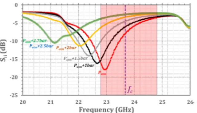
fres (GHz) fres fres. (1+0.013%) fres. (1–0.310%) fres. (1-0.349%) Measurement results at atmospheric pressure (Patm) give a resonant frequency close to 22.95
GHz (see Fig. 19). Simulation results with a 16µm-thick cavity and a 105µm-thick Si membrane are in agreement with the experimental data with a shift of around 150 MHz (0.7 % of fres). In addition, it can be noticed that the cavity thicknesses of 15 µm and 14 µm provide a frequency shift of 200 MHz (0.9 %) and of 350 MHz (1.5 %), respectively (see Table IV and Table V).
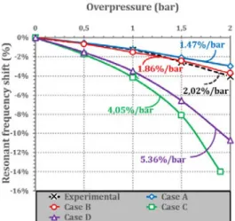
Fig. 15. Resonant frequency shift for various applied overpressures. Experimental data (dashed black line) and
results obtained in correspondence of the following four cases: Case A (blue line) where the electrical field E-field is maximum in x = XA for the corresponding displacement calculated through the close-form expression; Case B
(red line) where the electrical field E-field is maximum in x = XA for the corresponding displacement simulated
through COMSOL simulations; Case C (green line) where the membrane deflection is maximum in the centre of the membrane (x = 0) for the corresponding displacement calculated through the close-form expression, and Case D (purple line) where the membrane deformation is maximum at the center of the membrane (x = 0) for the corresponding displacement simulated through COMSOL. Sensitivities are given for each case and are calculated between 0 and 2bars.
Fig. 16. Input reflection coefficient Sii at fc = 23.8 GHz (radar operating frequency) as a function of overpressure:
comparison between the experimental data (dashed black line), the close-form expression results, and the COMSOL results (See Fig. 15 for the definition of Cases A, B, C and D). The parameters S and FSR denote respectively the sensitivity and the full-scale range of the sensor between 0 and 2 bars.
Fig. 17. Views of the packaged pressure
sensor.
Fig. 18. Experimental setup for measuring the scattering
parameters of the microwave sensor when a pressure is applied.
Fig. 19. Measured input reflection coefficient Sii versus
frequency for various applied overpressures.
These results validate the choice of 16µm in the electromagnetic simulation for the separation distance between the membrane and resonator. Fig. 19 also displays the variation of the reflection coefficient Sii for different overpressures applied on the sensor’s membrane.
The linear behavior of the input reflection coefficient of the microwave sensor between 1 bar and 2 bars depicted in Fig. 20 allows deriving the contact overpressure PC. The extrapolation of linear behavior at 2.54 dB (that is, when the membrane is in contact with the resonator) gives an overpressure
PC at 2.26 bars, which corresponds to the value obtained from COMSOL simulation (2.23 bars). It is also relevant to compare in Figs. 15 and 16 the experimental data with the simulated results obtained from the four cases defined in Section 5 (see cases A, B, C and D): the results obtained for the deflection in cases A and B (flat membrane model approximation) are in excellent agreement with the measurement data. Moreover, the sensitivity and full-scale range of the sensor between 0 and 2 bars are respectively of 2 % / bar (or equivalently, 460MHz / bar) and 4 % (930 MHz) for the resonant frequency (see Fig. 21). The best performances are obtained between 1 and 2 bars with a sensitivity of 2.7 % / bar (or equivalently, 620 MHz / bar) and a full-scale range of and 2.7 % (620 MHz). Moreover, when measuring
Sii parameter at the operating frequency fc (see Fig. 20), the sensitivity is of 1.86 dB/bar while the full-scale range is of 3.2 dB. Again, the best performances are obtained between 1 and 2 bars with the sensitivity of 2.29 dB/bar and a full-scale range of 2.29 dB. To the best knowledge of the authors, these results show the device is the most sensitive in comparison with the state-of-the-art (see Table I).
1. Conclusion
This paper described the design, manufacturing and characterization of a transducer dedicated to wireless measurement of pressure. The proposed EM passive and wireless pressure sensor brings a significant performance improvement compared the very first pressure sensor reported in 2007 [6]. A monolithic configuration using microstrip technology was proposed and allowed the manufacturing of packaged pressure sensors without spurious resonances. The analysis of the cavity thickness before and after the silicon membrane bonding, as well as the airtightness and the resilience to pressure hysteresis of the transducer, was reported and validated the technological process. Mechanical and electromagnetic simulation results were discussed and were found in very good agreement with experimental data. The future work will consist of remotely interrogating the fabricated pressure sensors by using the FMCW radar beam scanning technique reported in [5] and [17].
Acknowledgments
The authors wish to thank Occitanie Region (CARANUC Project) and EDF (Electricité de France) for financial support. This work was partly supported by LAAS-CNRS micro and nanotechnologies platform members of the French RENATECH network. We would like to thank Liliane Duperon for her proofreading of the paper.
Conflicts of Interest
The authors declare no conflict of interest. The founding sponsors had no role in the design of the study; in the collection, analyses, or interpretation of data; in the writing of the manuscript, and in the decision to publish results.
References
[1] P. Pons, H. Aubert, P. Ménini, M.–M. Tentzeris, Electromagnetic transduction for wireless passive sensors, Eurosensors, Sept 2012, Krakow, Poland.
[2] T. T. Thai, M. Jatlaoui, H. Aubert, P. Pons, G. R. Dejean, M. M. Tentzeris, R. Plana, A Novel Passive Wireless
Ultrasensitive Temperature RF Transducer for Remote Sensing, IEEE International Microwave Symposium,
Anaheim, California, USA, pp. 473-476, 23-28 May 2010.
[3] H. Hallil, P. Ménini, H. Aubert, Novel Microwave Gas Sensor Using Dielectric Resonator with SnO2 Sensitive
Layer, Eurosensors, Lausanne, Switzerland, 6–9 September, 2009.
[4] S. Bouaziz, F. Chebila, A. Traille, P. Pons, H. Aubert, M.-M. Tentzeris, Novel Micro-fluidic Structures for
Wireless Passive Temperature Telemetry Medical Systems Using Radar Interrogation Techniques in Ka-band, IEEE
Antennas and Wireless Propagation Letters, vol. 11, pp. 1706-1709, 2012.
[5] D. Henry, J.G.D. Hester, H. Aubert, P. Pons, M.-M. Tentzeris, Long Range Wireless Interrogation of Passive
Humidity Sensors using Van-Atta Cross-Polarization Effect and Different Beam Scanning Technique, IEEE
Transactions on Microwave Theory and Techniques, vol. 65, no. 12, pp. 5345-5354, December 2017. [6] M. Jatlaoui, F. Chebila, P. Pons, H. Aubert, Working Principle Description of the Wireless Passive EM
Transduction Pressure Sensor, European Physical Journal - Applied Physics, vol. 56, no. 1, oct 2011.
[7] A. Ibrahim, D. R. S. Cumming, Passive single chip wireless microwave pressure sensor, Sensors and Actuators A, Physics, Vol. 165, No. 2, pp. 200-206, February 2011.
Fig. 20. Measured input reflection coefficient Sii at
23.8 GHz (radar operating frequency) as a function of the applied overpressure.
Fig. 21. Measured resonant frequency shift for various
[8] D. E. Senior, X. Cheng, P. Jao, C. Kim, J. K. Kim, Y. Yoon, Wireless passive sensing application using a cavity
loaded evanescent mode half mode substrate integrated waveguide resonator, 2011 16th International Solid-State
Sensors, Actuators and Microsystems Conference, Beijing, 2011, pp. 2014-2017.
[9] H. Cheng, G. Shao, S. Ebadi, X. Ren, K. Harris, J. Liu, C. Xu, L. An, X. Gong, Evanescent-mode-resonator-based
and antenna-integrated wireless passive pressure sensors for harsh-environment applications, Sensors and Actuators
A, Physics, Vol. 220, 2014, pp. 22-33, ISSN 0924-4247.
[10] S. Su, F. Lu, G. Wu, D. Wu, Q. Tan, H. Dong, J. Xiong, Slot Antenna Integrated Re-Entrant Resonator Based
Wireless Pressure Sensor for High-Temperature Applications, Sensors (Basel),vol.17, no. 9, August 2017.
[11] J. E. Rogers, Y. K. Yoon, M. Sheplak, J. W. Judy, A Passive Wireless Microelectromechanical Pressure Sensor for
Harsh Environments, in Journal of Microelectromechanical Systems, vol. 27, no. 1, pp. 73-85, February 2018.
[12] P. Schumacher, C. Schuster, A. Jiménez-Saéz, M. Schüßler, R. Jakoby, Passive chipless wireless pressure sensor
for Harsh and reflective environments, German Microwave Conference (GeMiC), Freiburg, pp. 227-230,
Germany, 2018.
[13] https://www.ansys.com/products/electronics/ansys-hfss
[14] A. Boukabache, Ph. Menini, P. Pons, Microcapteurs de pression, Technique de l’ingénieur, R2070-1/R2070-9. [15] D. Mingli, M. M. Jatlaoui, P. Pons, H. Aubert, Multiphysic Simulations Approach for an EM Transduction Based
Pressure Sensor, Micromechanics and Microsystems Europe Workshop (MME) 2009, Toulouse.
[16] https://www.comsol.com/
[17] J. Philippe, D. Henry, M. V. De Paolis, A. Rumeau, A. Coustou, S. Charlot, P. Pons, H. Aubert, Wireless
remote monitoring of packaged passive sensor for in-situ pressure measerement in highly reflective environments,
International Microwave Symposium, Philadelphia, United States of America, 10-15 Jun 2018.
Biographies
Julien PHILIPPE received the M.S. degree in microelectronics and nanotechnology from the Grenoble INP
PHELMA, France, in 2011. He received the Ph.D. degree in nanoelectronics and nanotechnologies from the Grenoble Alpes University, France, in 2014. His work was focused on the conception, characterization and development of co-integrated NEMS (Nano Electro Mechanical Systems) – CMOS cells for gas sensing and mass spectrometry application. In February 2016 he was contracted as a Post-Doctoral Researcher in the research laboratory of analysis and architecture of systems (LAAS-CNRS) of Toulouse, France. He currently works on the fabrication and characterization of passive RF sensors based on millimeter wave transducers for wireless monitoring of physical properties.
Maria Valeria DE PAOLIS received the M.S. degree in telecommunications engineering (cum laude) from the
University of Salento, Lecce, Italy, in 2014. In 2017, she finished the Ph.D. course in Engineering of Complex Systems at the University of Salento. Her work was focused on the design, characterization, and fabrication of wireless power transfer systems. In November 2017, she was contracted as a Post-Doctoral Researcher in the research laboratory of analysis and architecture of systems (LAAS-CNRS) of Toulouse, France. Her research activity is currently focused on the design and characterization of RF sensors.
Cristina ARENAS-BUENDIA received the M.S. degree in hyperfrequency and electronics from the Universitat
Politècnica de València (UPV), Spain, and Télécom Bretagne, Brest, France, respectively, in 2012. She received the Ph.D. degree in Electronics from Télécom Bretagne and from UPV in 2016. Her main research interests are focused on the design of passive components on gap waveguide technology, multilayer technology and fluid characterization in the millimeter-wave band. In 2016, she was contracted as a Post-Doctoral Researcher in the CNRS-LAAS (Toulouse, France). Her research interest was the RF pressure sensors design and validation. Currently, she works in Thales Alenia Space (Toulouse, France) as RF engineer.
Dominique HENRY received the M.S. degree in electronical engineering from the INP ENSEEIHT, Toulouse,
France, in 2012. From 2013 to 2014, he was a research engineer at LAAS-CNRS, Toulouse, France. He started a PhD in 2014 in collaboration with LAAS-CNRS and Ovalie-Innovation, Auch, France. His research interest includes use of microwave radars for precision agriculture, the remote sensing of passive sensors, development of radar interrogation techniques and smart antennas in constraint environments, microwave imaging and signal processing.
Antony COUSTOU was born in Brive, France, in 1973. He received the Ph.D. degree in microwave circuit design
and microelectronics from the Paul Sabatier University of Toulouse, France, in 2001. His doctoral dissertation concerned the design of MMIC on BiCMOS SiGe technology in the X band frequency range. In January 2002, he joined the research laboratory of analysis and architecture of systems (LAAS-CNRS) of Toulouse, France, where he is currently an RF systems design engineer. His research interest is the design of new architectures of RF systems in the field of millimeter wave for remote sensing and telecommunication networks.
Alexandre RUMEAU was born in Limoges, France in 1984. He received the B.S. degree in electronics at Lycée
Déodat de Séverac in Toulouse, France, in 2006. He started working on microwave measurements and electrical characterization at Laboratoire d’Architecture et d’Analyse des Systèmes (LAAS-CNRS), Toulouse, France, in March 2008. His main activities consist of microwave measurements, antennas measurements, and more especially with probe stations and microelectronics characterization bench, including cryogenic probe station. He is in charge of the microwave area within the characterization platform of the LAAS-CNRS, ensuring the proper functioning of the equipments and the training of the new users.
Hervé AUBERT is Professor at the Institut National Polytechnique (INPT), Toulouse, France, and is the Head of
the Micro- and Nano-systems for Wireless Communications Research Group at the Laboratory for the Analysis and Architecture of Systems (LAAS), National Center for Scientific Research (CNRS), Toulouse, France. Currently, his research activities involve the electromagnetic modelling of complex (multi-scale) structures and the design of zero-power wireless electromagnetic sensors.
Patrick PONS received his Ph.D. degree in electronics in 1990 on silicon pressure micro-sensors. Since 1991 he is a
researcher in the CNRS-LAAS (National Scientific Research Center – Laboratory of Analysis and Analysis of Systems) in Toulouse. His research interests are focused in micro-technologies and micro-sensors. In 2005 he started research at LAAS in a new field coupling micro-sensors and electromagnetic for the development of passive wireless sensors. Concepts of pressure, temperature, stress and nuclear radiation sensors have been validated with radar interrogation. Dr. Patrick PONS is author or co-author of more than 95 papers in referred International Journals and more than 267 communications in International Conferences.


![Fig. 13. Simulated total displacement [µm] for an applied overpressure of 1 bar. The mechanical simulations were performed by using COMSOL Multiphysics software [16]](https://thumb-eu.123doks.com/thumbv2/123doknet/14423669.513798/8.892.290.614.895.1088/simulated-displacement-overpressure-mechanical-simulations-performed-multiphysics-software.webp)
![Fig. 14. Membrane deflection as a function of the applied overpressure P obtained from the close-form expression of Eq.(1) and from COMSOL Multiphysics simulations [16]: a) displacement [µm] versus the applied overpressure [bar] at the center of the ci](https://thumb-eu.123doks.com/thumbv2/123doknet/14423669.513798/9.892.140.739.102.313/membrane-deflection-overpressure-expression-multiphysics-simulations-displacement-overpressure.webp)