Concept Synthesis and Design Optimization of Meso-scale, Multi-Degree-of-Freedom Precision Flexure Motion Systems with Integrated Strain-based Sensors
by
Christopher M. DiBiasio
Sc.M., Mechanical Engineering (2007) Massachusetts Institute of Technology Sc.B., Mechanical Engineering (2005) Massachusetts Institute of Technology
Submitted to the Department of Mechanical Engineering in Partial Fulfillment of the Requirements for the Degree of
Doctor of Philosophy in Mechanical Engineering at the
Massachusetts Institute of Technology June 2010
2010 Massachusetts Institute of Technology All rights reserved.
Signature of Author……… Department of Mechanical Engineering February 12, 2010
Certified by……… Martin L. Culpepper Associate Professor of Mechanical Engineering
Thesis Supervisor
Accepted by……...……… David Hardt Ralph E. and Eloise F. Cross Professor of Mechanical Engineering Graduate Officer
Concept Synthesis and Design Optimization of Meso-scale, Multi-Degree-of-Freedom Precision Flexure Motion Systems with Integrated Strain-based Sensors
by
Christopher M. DiBiasio
Submitted to the Department of Mechanical Engineering on February 12, 2010 in Partial Fulfillment of the Requirements for the Degree of Doctor of Philosophy in
Mechanical Engineering
ABSTRACT
The purpose of this research was to generate the knowledge required to 1) identify where and how to best place strain-based sensors in multi-degree-of-freedom (MDOF) flexure systems and 2) design a flexure system with optimal topology/size/shape for precision equipment and instrumentation. The success of many application areas (e.g. probe-based nanomanufacturing) hinges on the ability to design and realize low-cost, high-performance MDOF nanopositioners. The repeatability and accuracy of precision flexure-based instruments depends upon the performance of the flexure mechanism (e.g. bearings, actuators, and structural elements) and a metrology system (e.g. sensors). In meso-scale MDOF nanopositioners the sensing system must be integrated into the structure of the nanopositioner. The only viable candidate for small-scale, low-cost sensing is strain-based sensors; specifically piezoresistive sensors.
Strain-based sensing introduces strong coupling and competition between the metrology and mechanical subsystems because these subsystems share a load path. Traditional tools for flexure system and compliant mechanism synthesis are not capable of simultaneously optimizing the mechanical and sensing subsystems. The building block synthesis approach developed in this work is the only tool capable of designing compliant mechanisms with integrated strain based sensing. Building block modeling allows for rapid synthesis and vetting of concepts. This approach also allows the designer to check concept feasibility, identify performance limits and tradeoffs, and obtain 1st order estimates of beam geometry. In short, this enables one to find an optimal design and set first order design parameters.
The utility of the preceding is demonstrated via a case study. A meso-scale 6-DOF nanopositioner was designed via the building block synthesis approach. Polysilicon piezoresistors were surface micromachined onto a microfabricated silicon nanopositioner. The nanopositioner was actuated with moving magnet Lorentz force actuators. The final prototype costs less than $300 US and was found to have 10’s of µm range, nm-level resolution, and a 100 Hz 1st mode. The accuracy of the sensing system as determined by existing metrology equipment is better than 17% in-plane and better than 30% out-of-plane.
Thesis Supervisor: Martin L. Culpepper
ACKNOWLEDGEMENTS
I would first like to thank my thesis advisor, Professor Martin Culpepper. Marty has served as a mentor to me throughout my entire MIT career. He has never accepted mediocrity from me and has always pushed me to perform at my highest level. I am forever grateful for the lessons he has taught me throughout the years. I would also like to thank Marty for giving me the financial and intellectual freedom to allow me to pursue a thesis topic of my interest instead of necessity. Finally, Marty has played an important role in my life over the last decade and I hope to continue my friendship with him over the years to come.
I would like to thank the members of my thesis committee, Professors Ian Hunter and Jeff Lang, for all of the guidance they have given me. Every question, comment, and critique made this work stronger in the end.
Many thanks go out to the following people and organizations that donated time and resources to me during my research: Professor Jim Lee at OSU who provided project funding (via NSF) and support, NanoInk for DPN materials, Professor Dennis Freeman for the use of his MMA metrology equipment, Daisuke Ike for his help with COMSOL simulation, Maria Telleria for her help fabricating the DPN machining center, and Robert Panas for his help with the sensing and actuation electronics. I would like to thank Dr. Dariusz Golda and Dr. Shih Chi Chen for taking the time to discuss prototype microfabrication and use of the MMA metrology system. Finally, I would like to thank Michael Cullinan for his help microfabricating, testing, and analyzing the data from the final prototype.
Thanks to all my LMP and PCSL colleagues, past and present, for the help and support given to me during my doctoral research. All of you gave made the LMP and PCSL special places to me that I will never forget. Additionally, special thanks go to Thor Eusner for helping me to relax, have fun, and enjoy my time in graduate school.
Finally, I would like to thank all of the friends and family that have touched me throughout the years. I could always count on every single one of you to help pick me up when I had a setback. I am eternally grateful to all of you for your support. To my brother Kevin and my soon to be sister-in-law Melanie, thanks for being there and helping me look at the lighter side of things.
To my girlfriend Kasey, thank you for being in my life. I don’t know how I would have survived the last year of my doctoral program without you. Finally, I would like to thank my parents for all of their unwavering love and support. You instilled in me a thirst for knowledge as well as a hard work ethic as a child, and I know that played a large role in the successes I enjoy today. I continue to try my hardest each and every day to make you proud.
Table of Contents
Abstract ... 3 Table of Contents... 7 List of Figures ... 13 List of Figures ... 13 List of Tables ... 19 Chapter 1 Introduction ... 23 1.1 Importance ... 261.1.1 Nano-scale Manufacturing and Metrology ... 27
1.1.2 Role of Nanopositioners in Nano-scale Manufacturing/Metrology... 28
1.1.3 Six Degree-of-Freedom Nanopositioner Architecture... 31
1.1.4 Flexure Bearings for Meso- and Micro-scale Nanopositioners ... 33
1.1.5 Actuators for Meso- and Micro-scale Nanopositioners ... 33
1.1.6 Need for Sensing in Nanopositioners ... 35
1.1.7 Main Challenges in Designing Meso- and Micro-scale Nanopositioners... 35
1.2 Overview of Prior Art ... 37
1.2.1 Sensors ... 37
1.2.1.1 Capacitive Sensors ... 38
1.2.1.2 Hall Effect Sensors ... 40
1.2.1.3 Inductance / Eddy Current Sensors... 41
1.2.1.4 Interferometry ... 42
1.2.1.6 Strain Sensors... 43
1.2.1.7 Choice of Sensor for Meso- and Micro-scale Nanopositioners ... 43
1.2.2 Flexural Mechanism Design Tools ... 44
1.2.2.1 Topology Synthesis... 44
1.2.2.2 Psuedo-rigid-body Modeling ... 46
1.2.2.3 Exact Constraint Design ... 47
1.2.2.4 Relevance of Prior Art ... 48
1.3 Scope... 49
1.3.1 Fundamental Issues ... 50
1.3.2 Case Study ... 53
1.3.3 Thesis Outline ... 56
Chapter 2 Background on Strain Sensing ... 57
2.1 Physics of Strain Sensing... 57
2.1.1 Physics of Flexure Beams ... 57
2.1.2 Silicon as a Mechanical Material ... 62
2.1.3 Properties of Thin Films ... 63
2.1.4 Physics of Strain Sensors ... 65
2.1.4.1 Poisson Effect Strain Gages... 65
2.1.4.2 Piezoresistive Strain Gages... 66
2.1.5 Competition between Flexure Bearings and Strain Sensors ... 74
2.2 Strain Sensor Sensitivity and Noise... 74
2.3 Sensing Electronics... 79
Chapter 3 Building Block Modeling and Synthesis... 87
3.1 Flexure Element Models... 87
3.1.1 Fixed-Free Cantilever with Transverse Force... 88
3.1.2 Fixed-Guided Cantilever with Transverse Force ... 96
3.1.3 Fixed-Free Cantilever with End Moment ... 98
3.1.4 Fixed-Pinned Beam with End Moment... 99
3.1.5 Technology Specific Equation Forms... 100
3.1.6 Effect of Averaging on System Noise ... 103
3.1.7 Element Model Summary ... 104
3.2 Series and Parallel Addition ... 105
3.2.1 Parallel Element Addition... 105
3.2.2 Series Element Addition ... 106
3.2.3 System Model Summary... 109
3.3 Flexure Synthesis Example... 109
Chapter 4 Design and Optimization... 113
4.1 Case Study Introduction... 113
4.2 System Architecture... 114
4.3 HexFlex Architecture... 115
4.4 HexFlex Design ... 117
4.4.1 Maximum Performance Analysis... 118
4.4.2 Local Displacement Analysis ... 119
4.4.3 Global Displacement Analysis... 120
4.4.5 Concept Optimization ... 122
4.5 Lorentz Force Actuators ... 123
4.6 Sensing System Design... 125
4.7 Simulated Performance... 128
Chapter 5 System Fabrication... 131
5.1 Microfabrication ... 131
5.1.1 Microfabrication Process ... 131
5.1.2 DRIE Process Notes... 136
5.1.3 Metal to Polysilicon Interface Notes... 137
5.2 Sensing Electronics... 138
5.3 Actuation Electronics... 140
5.4 Calibration Fixture... 141
Chapter 6 Experimental Results and Discussion ... 143
6.1 Quasi-static Performance ... 143
6.1.1 MEMS Motion Analyzer ... 143
6.1.2 Testing Procedure ... 145 6.1.3 Stage Motion ... 148 6.1.4 Sensor Response ... 151 6.1.5 Nanopositioner Performance ... 153 6.1.6 Calibration Matrix... 154 6.1.7 System Repeatability ... 156 6.2 Dynamic Performance ... 157 6.3 Thermal Sensitivity... 158
6.4 Open Loop DPN Writing... 159
6.5 Summary of Results... 159
Chapter 7 Summary and Future Work ... 161
7.1 Summary... 162
7.2 Future Work ... 166
7.2.1 Improving Calibration Equipment ... 166
7.2.2 Improving Sensor Performance ... 167
7.2.3 Improving Nanopositioner Performance... 168
7.2.4 Integration into a Probe-based Nanomanufacturing Line ... 168
References... 171
Appendix A Photomasks... 179
A.1 Mask 1 – Polysilicon Etch ... 179
A.2 Mask 2 – Aluminum Etch ... 179
A.3 Mask 3 – DRIE ... 182
A.4 Alignment Marks ... 182
A.5 Resistor to Trace Connection Detail ... 182
Appendix B Design of the Precision Bridge Circuit... 185
B.1 Precision Voltage Reference ... 186
B.1.1 Low Voltage Configuration... 187
B.1.2 High Voltage Configuration... 188
B.2 Wheatstone Bridge ... 188
B.2.1 Quarter Bridge Configuration ... 189
B.2.3 Full Bridge Configuration ... 190
B.2.4 Span Temperature Compensation ... 190
B.2.5 Proper Cable Shielding... 190
B.3 Signal Amplifier... 190
B.3.1 Instrumentation Amplifier Selection ... 190
B.3.2 Adjustable Reference Voltage Circuit Design ... 191
B.4 Optional Filter ... 192
List of Figures
Figure 1.1: Traditional approach versus building block approach for designing flexure
systems... 24
Figure 1.2: Prototype six-axis, microfabricated nanopositioner with integrated piezoresistive sensors... 26
Figure 1.3: Impact of parallelism errors between a surface tool and a workpiece. ... 29
Figure 1.4: Massively parallel DPN array containing 55,000 probe tips. ... 29
Figure 1.5: State-of-the-art six-axis nanopositioners from Physik Instrumente. ... 31
Figure 1.6: Compliant HexFlex nanopositioner (a) and required actuator combinations to achieve six-axis motion (b)... 32
Figure 1.7: A compliant parallel-guiding mechanism. ... 33
Figure 1.8: A six-axis force/displacement sensor with parallel plate and comb-drive capacitive sensors. ... 38
Figure 1.9: Dynamic range versus characteristic footprint for different sensing technologies. ... 44
Figure 1.10: Design domain for topological synthesis and resulting topology after computer iteration. ... 45
Figure 1.11: Parallel guiding mechanism and its PRB equivalent... 46
Figure 1.12: Exact constraint of a block for multiple degrees of freedom. ... 48
Figure 1.13: Examples of flexural building blocks (a) and the parallel addition of two flexural building blocks to create a flexural topology. ... 51
Figure 1.14: Graphical representation of SNR as a function of parallel guiding mechanism bandwidth and dynamic range. ... 51
Figure 1.16: 55,000 DPN tip array mounted onto a meso-scale HexFlex nanopositioner. ... 55
Figure 2.1: Euler-Bernoulli notation for cantilever beam bending... 58
Figure 2.2: Four main types of flexural building blocks. ... 59
Figure 2.3: LPCVD thin film strain as a function of anneal time and temperature. ... 64
Figure 2.4: Silicon piezoresistive coefficients for (a) p-type and (b) n-type silicon. ... 69
Figure 2.5: Piezoresistive correction factor for (a) p-type and (b) n-type silicon. ... 70
Figure 2.6: Polysilicon gage factor as a function of doping concentration. ... 71
Figure 2.7: Polysilicon gage factor as a function of grain size for p-type doping. ... 72
Figure 2.8: Polysilicon gage factor as a function of anneal temperature. ... 73
Figure 2.9: αTCR for p-type and n-type silicon as a function of doping. ... 75
Figure 2.10: αTCR and αGF for p-type (a) and n-type (b) polysilicon as a function of doping. ... 75
Figure 2.11: Hooge constant for silicon as a function of anneal temperature. Data taken from Vandamme et al [2.34]... 78
Figure 2.12: Three configurations of a Wheatstone bridge. Arrows indicate whether or not a sensor sees an increase or decrease in resistance due to an applied strain. Black boxes indicate measurement resistors while white boxes indicate balancing resistors. ... 79
Figure 2.13: AFM tip with integrated piezoresistors. ... 81
Figure 2.14: High resolution cantilever beam. ... 82
Figure 2.15: Force sensing cantilever beam. ... 82
Figure 2.16: Zeiss F25 micro-stylus probe. ... 83
Figure 2.17: Bistable mechanism with integrated sensing. ... 83
Figure 2.18: Dual axis sensing AFM cantilever. ... 84
Figure 3.1: SNRmin,DR versus dynamic range for an n-type silicon piezoresistor.
Piezoresistors are assumed to be n-type polysilicon with a resistance of 3kΩ arranged in a ¼ bridge driven at 10 V. The gage factor is assumed to be -107 and the safety
factor is 3... 92
Figure 3.2: Maximum range as function of resolution for n-type silicon piezoresistors... 93
Figure 3.3: Flexure beam length required to achieve desired resolution for h = 100 µm... 95
Figure 3.4: End moment applied to a free-free cantilever beam in a frame. ... 98
Figure 3.5: SNRmin,DR for a Johnson noise limited sensor (a) and a flicker noise limited sensor (b) for a system with a mechanical bandwidth of 50 Hz. ... 102
Figure 3.6: Effect of averaging on total sensor noise. ... 104
Figure 3.7: Parallel addition of two fixed-guided beams to produce a clamped-clamped beam... 105
Figure 3.8: Parallel addition of two fixed-free beams to produce a series folded flexure. ... 107
Figure 3.9: Building block synthesis procedure. ... 109
Figure 3.10: Concepts analyzed for the single DOF stage example. ... 110
Figure 4.1: Architecture of the DPN nanomanufacturing center. ... 115
Figure 4.2: HexFlex architecture and nomenclature... 116
Figure 4.3: Candidate topologies for the meso-scale HexFlex nanopositioner. ... 117
Figure 4.4: Coil configurations. ... 123
Figure 4.5: Sensor configuration for the HexFlex prototype. ... 126
Figure 5.1: Stage displacement as a function of actuator input. ... 141
Figure 5.2: Exploded CAD image of the calibration fixture (a) and an image of the as-fabricated fixture (b). ... 142
Figure 6.2: Target image and corresponding ROI used for motion analysis. ... 145
Figure 6.3: System diagram for the experimental setup. ... 146
Figure 6.4: Motion of the HexFlex stage in response to a commanded motion in the x axis during a single calibration test. ... 148
Figure 6.5: Motion of the HexFlex stage in response to a commanded motion in the x axis during four calibration tests. ... 150
Figure 6.6: Bridge output from each sensor during a commanded motion in the x axis. ... 152
Figure 6.7: Frequency response of the stage for a commanded θz motion. ... 157
Figure 6.8: Change in sensor output voltage as a function of temperature... 158
Figure 6.9: Lateral force microscopy scan of DPN dot pattern printed with an open-loop HexFlex prototype on a gold substrate. ... 159
Figure 7.1: Final meso-scale HexFlex prototype loaded in the calibration frame... 162
Figure A.1: Wafer (a) and die (b) level views of Mask 1. The square in (a) is 18 cm on a side while the diameter in (b) is approximately 3.6 cm. ... 180
Figure A.2: Wafer (a) and die (b) level views of Mask 2. The square in (a) is 18 cm on a side while the diameter in (b) is approximately 36 cm. ... 181
Figure A.3: Wafer (a) and die (b) level views of Mask 3. The square in (a) is 18 cm on a side while the diameter in (b) is approximately 36 cm. ... 183
Figure A.4: Alignment marks used on Mask 1 and 3 (a) and Mask 2 (b). ... 184
Figure A.5: Detail of the piezoresistors and metal traces located on each flexure beam. The flexure beam in (c) is 200 µm wide. ... 184
Figure B.1: Diagram of the precision bridge circuit. ... 186
Figure B.2: TI uA723 schematic for <7 V operation (a) and >7 V operation (b)... 187
Figure B.3: Wheatstone bridge schematic. ... 189
Figure B.5: Schematic of the precision bridge circuit. ... 193 Figure B.6: Layout of the precision bridge circuit... 194
List of Tables
Table 1.1: Nanopositioner requirements for nanomanufacturing/metrology applications. ... 30
Table 1.2: Commercially available 6-DOF nanopositioner performance... 31
Table 1.3: Typical small-scale actuator performance. ... 34
Table 1.4: Required parallel plate area for different range/resolution requirements... 39
Table 1.5: Required number of comb fingers for different range/resolution requirements... 40
Table 1.6: Case study nanopositioner requirements. ... 55
Table 2.1: Maximum axial stress for the four main types of flexural elements. ... 60
Table 2.2: Mechanical properties of common MEMS materials... 62
Table 2.3: Attenuation of applied piezoresistor strain as a function of oxide thickness. ... 63
Table 2.4: Gage factor for three common metallic strain gage materials. ... 66
Table 2.5: Piezoresistive coefficient values for silicon as a function of doping... 68
Table 2.6: Piezoresistive coefficient values for polysilicon as a function of doping. ... 72
Table 2.7: Sensitivity of resistivity to temperature for three common metallic strain gage materials at room temperature [2.13]... 74
Table 3.1: Material properties for flexures and sensors in the synthesis example. ... 111
Table 4.1: Case study nanopositioner requirements. ... 114
Table 4.2: Normalized actuator commands to actuate the specific displacements of the HexFlex... 116
Table 4.3: Material properties for the polysilicon sensors and silicon flexures used in fabricating the HexFlex used for the case study. ... 118
Table 4.4: Relation of local flexure chain displacements to global stage displacements
(θ = 30o). ... 120
Table 4.5: Best case performance of the two concepts versus the system functional requirements... 121
Table 4.6: Coil design parameters. ... 124
Table 4.7: Simulated performance of the final HexFlex prototype. ... 128
Table 4.8: Simulated dynamic performance of the first four modes of HexFlex prototype. ... 129
Table 5.1: Process plan for the microfabrication of the HexFlex nanopositioner. ... 132
Table 5.2: Processing notes for the final approved process plan. ... 134
Table 5.3: Resistance of each tested sensor (including metal to polysilicon contact resistance) in the final prototype after annealing. Sensor numbering is the same as in Fig. 4.5. ... 138
Table 5.4: Background electronics noise for each bridge channel. ... 139
Table 5.5: Energizing voltage and amplifier gain for each bridge circuit channel... 139
Table 5.6: Energizing voltage and amplifier gain for each bridge circuit channel... 140
Table 6.1: MMA output voltage for each channel during quasi-static testing... 146
Table 6.2: MMA motion capture settings. ... 147
Table 6.3: Results of the linear fit for each motion during a commanded motion in the x axis. Results are for a single calibration test on sensors 3 and 6. ... 149
Table 6.4: Results of the linear fit for each motion during a commanded motion in the x axis. Results are from all four calibration experiments. ... 151
Table 6.5: Linear fit of bridge output for each sensor to x axis motion during commanded motion in the x axis. ... 153
Table 6.6: Range, resolution and accuracy of the sensing system integrated into the HexFlex prototype. ... 154
Table 7.1: Case study nanopositioner requirements. ... 165 Table C.1: Sensor output due to a commanded motion in the x direction and an initial
temperature of 24.75 C. ... 196 Table C.2: Sensor output due to a commanded motion in the y direction and an initial
temperature of 24.71 C. ... 197 Table C.3: Sensor output due to a commanded motion in the θz direction and an initial
temperature of 24.45 C. ... 198 Table C.4: Sensor output due to a commanded motion in the z direction and an initial
temperature of 24.03 C. ... 199 Table C.5: Sensor output due to a commanded motion in the θx direction and an initial
temperature of 24.25 C. ... 200 Table C.6: Sensor output due to a commanded motion in the θy direction and an initial
temperature of 23.66 C. ... 201 Table C.7: Sensor output due to a commanded motion in the x direction and an initial
temperature of 23.95 C. ... 202 Table C.8: Sensor output due to a commanded motion in the y direction and an initial
temperature of 23.88 C. ... 203 Table C.9: Sensor output due to a commanded motion in the θz direction and an initial
temperature of 23.77 C. ... 204 Table C.10: Sensor output due to a commanded motion in the z direction and an initial
temperature of 24.05 C. ... 205 Table C.11: Sensor output due to a commanded motion in the θx direction and an initial
temperature of 24.13 C. ... 206 Table C.12: Sensor output due to a commanded motion in the θy direction and an initial
Table C.13: Sensor output due to a commanded motion in the x direction and an initial
temperature of 25.55 C. ... 208 Table C.14: Sensor output due to a commanded motion in the y direction and an initial
temperature of 25.52 C. ... 209 Table C.15: Sensor output due to a commanded motion in the θz direction and an initial
temperature of 25.49 C. ... 210 Table C.16: Sensor output due to a commanded motion in the z direction and an initial
temperature of 25.45 C. ... 211 Table C.17: Sensor output due to a commanded motion in the θx direction and an initial
temperature of 25.54 C. ... 212 Table C.18: Sensor output due to a commanded motion in the θy direction and an initial
temperature of 25.45 C. ... 213 Table C.19: Sensor output due to a commanded motion in the x direction and an initial
temperature of 23.58 C. ... 214 Table C.20: Sensor output due to a commanded motion in the y direction and an initial
temperature of 23.68 C. ... 215 Table C.21: Sensor output due to a commanded motion in the θz direction and an initial
temperature of 23.73 C. ... 216 Table C.22: Sensor output due to a commanded motion in the z direction and an initial
temperature of 23.96 C. ... 217 Table C.23: Sensor output due to a commanded motion in the θx direction and an initial
temperature of 24.02 C. ... 218 Table C.24: Sensor output due to a commanded motion in the θy direction and an initial
Chapter 1
Introduction
The purpose of this research is to generate the knowledge required to 1) design a flexure system with optimal topology/size/shape and 2) identify where and how to best place strain-based sensors in multi-axis flexure systems for use in precision nanopositioners and instrumentation. The repeatability and accuracy of precision flexure-based instruments depend upon the performance of the flexure mechanism (e.g. bearings, actuators, and structural elements) and a metrology system (e.g. sensors). When strain-based sensing is used, there is strong coupling and competition between the metrology subsystem and the mechanical subsystem (e.g. range, resolution, bandwidth, stiffness, and load capacity) as the performance of these subsystems is subject to a shared load path. This coupling makes it difficult to perform early stage system design as the number of relevant variables are cumbersome to manage without time intensive iteration/computer modeling. This problem is even more troublesome in the design of multiple degree-of-freedom (MDOF) flexure systems.
Overcoming the limitations associated with subsystem coupling is important because many small-scale (i.e. meso- and micro-scale) MDOF flexure systems for precision nanopositioning/instrumentation cannot be realized without strain-based sensing. There is no body of knowledge that provides best principles and practices to guide designers during early-stage system design. This knowledge gap is problematic given the increasing desire to use closed-loop, small-scale flexure stages for nano-scale fabrication (e.g. probe-based manufacturing), nano-scale metrology (e.g. AFM, STM, SPM), and biological applications (e.g. protein and DNA probing/manipulation). These applications are difficult or impossible to realize as it is not possible to engineer these systems in a practical way.
Traditional design approaches, shown in Fig. 1.1(a), for closed-loop controlled, small-scale, MDOF flexure systems are at best cumbersome and iterative.
Pick Flexure
Topology
Predict Performance
via 1
stOrder
Modeling
Estimate Beam
Properties
Concept
Optimization via FEA
Specify Kinematics
and Functional Req’s
Pick Flexure
Topology
Predict Performance
via 1
stOrder
Modeling
Estimate Beam
Properties
Concept
Optimization via FEA
Compare Concepts,
Choose Final Design
Specify Kinematics
and Functional Req’s
Pick Flexure Building
Block
Use Series/Parallel
Rules to Find
Flexure Topology
Performance
Model Element
Performance
Final Concept
Optimization via FEA
(a) (b)
Figure 1.1: Traditional approach versus building block approach for designing flexure systems.
This research will focus on a new building block design approach, shown in Fig. 1.1(b), and its corresponding performance metrics for concept synthesis and modeling during early stage design. The goals of this building block approach are to:
1. Quantify the mechanical and sensing performance metrics of individual flexural building blocks
2. Develop rules that illustrate how these metrics change when building blocks are combined in series and parallel
This knowledge would allow designers to more rapidly/easily synthesize and vet first order concepts. Graphical representations of relative metrics contain large amounts of information regarding the coupling, sensitivity, and relationship between these metrics, however, they are often used in an ad hoc manner.
This research will focus on characterizing flexural building blocks by first identifying the relevant performance metrics and then graphically displaying the coupling of these metrics to help designers:
1. Locate global maxima and minima for each performance specification, 2. Understand the coupling between different metrics
3. Identify the corresponding tradeoffs
4. Enable a broader community of engineers to design high performance precision flexures The hypothesis is that this approach may be used to drive the early stages of design without the undue complication of computationally intense tools that yield high-performance designs that are not always practical or optimal solutions. The weakness of computer-based synthesis tools is that their results are 1) only “as good” as the rules that are programmed into them and 2) limited in their inventive capacity due to inflexible rules. This is acknowledged by those who initiated computer-based flexure synthesis [1.1, 1.2]. The current trend in computer-based flexure synthesis is to incorporate a building block approach with computer optimization [1.1, 1.2]. The building block approach, currently used in precision machine design, is known for its ability to generate the simplest and best solutions. The proposed approach is rooted in precision engineering philosophy [1.3-1.5] and retains the designer’s experience, knowledge, and abstract thinking ability in the design loop and therefore produces novel/practical solutions that often would not fall within the “rules” of a computer simulation. These benefits of retaining the designer in early stage design decision making have been recognized by the founders of computer-driven flexure synthesis [1.1, 1.2]. Further research is needed in order to understand the best way to use the building block approach, its limitations, and the improvements it offers over other approaches to flexure synthesis. Success in this research will lead to the following major contributions:
1. A building block synthesis approach for flexure-based precision instruments with integrated strain sensing that enables one to more easily and rapidly synthesize, model, and vet first order concepts
2. The building block synthesis and optimization of a self-sensing, six-axis, meso-scale nanopositioner with nanometer-level resolution and accuracy
3. The fabrication and calibration of a self-sensing, six-axis, meso-scale nanopositioner with nanometer-level resolution and accuracy
4. Guidelines and design rules that capture relevant microfabrication and integration considerations in early stage design for meso-scale precision instruments with integrated piezoresistive sensing
The major contributions of this research will be demonstrated via the design and fabrication of a microfabricated, meso-scale, 6-axis nanopositioner with integrated polysilicon piezoresistive strain sensors. This nanopositioner, shown in Fig. 1.2, costs less than $300 US and is capable of nanometer-level resolution and 10’s of microns of range.
Figure 1.2: Prototype six-axis, microfabricated nanopositioner with integrated piezoresistive sensors.
1.1 Importance
Finding ways to make, manipulate, and measure nanometer-scale features has been the focus of many research efforts over the last decade. The ability to create and interact with nanometer-level features has a wide range of applications such as medicine [1.6], chemical sensing [1.7], energy storage [1.8], and electronics [1.9]. The capability of nanopositioners, a specific type of precision instrument, to orient and position samples and tools with nanometer-level accuracy is
important to the realization of these applications. For the past decade the tools for nanopositioning have been application specific, low-volume, high-cost precision instruments. To realize next generation nanometer-level fabrication and metrology equipment nanopositioners must be made low-cost and more flexible for use in.
1.1.1 Nano-scale Manufacturing and Metrology
High-performance precision machines are required to make, manipulate, and measure nanometer-scale features. Conventional lithography processes used in the making of integrated circuits, micro-electrical-mechanical systems (MEMS), and sub-micron surface features are not capable of creating nanometer-scale features due to diffraction limitations. The inability of state-of-the-art manufacturing equipment to create and interact with nanometer-scale features requires new types of machines and instruments. These new instruments would enable many nano-scale applications including:
•Probe-based nanomanufacturing processes such as dip-pen nanolithography (DPN) [1.10] and nano-EDM (nEDM) [1.11]
•High volume nanoimprint nanolithography (NIL) [1.12] •Nozzle-based micro-/nano-printing [1.13]
•Video rate probe-based metrology such as atomic force microscopy (AFM), scanning tunneling microscopy (STM), and scanning probe microscopy (SPM) [1.14]
•Integrated circuit interconnect repair [1.15]
•Pick-and-place assembly of carbon nanotubes for nanoelectronics and nano-electrical-mechanical systems (NEMS) [1.16]
•Self-assembly of quantum dots for nanoelectronics [1.17] •High density data storage [1.18]
•Production of energy storage elements [1.8]
•Production of MEMS/NEMS chemical sensors [1.7] •In vivo cellular biopsy [1.19]
•Protein manipulation [1.20]
•In vivo biological force testing [1.21]
There have been many efforts to identify, develop, and refine processes and techniques for making, manipulating, and measuring nanometer-scale features. Candidate processes include DPN, NIL, e-beam [1.24], ion beam [1.25], SPM lithography [1.26], STM lithography [1.27], nEDM, AFM, STM, and SPM. The machines and instruments that are used for these processes are generally application-specific and designed to operate on one sample at a time. They have not been engineered for medium- or high-volume production and require setup times ranging from tens of minutes to a few hours before a sample can be processed. Furthermore, most of the machines and instruments that have been designed for these processes control a single probe tip or a single beam. Multiple probe tips or beams must be used in order to increase the production rate of these processes. Unfortunately, current machines and instruments are not capable of this.
1.1.2 Role of Nanopositioners in Nano-scale Manufacturing/Metrology
Nanopositioners are precision instruments designed to orient and position a tool, workpiece, or sample with nanometer precision. They must be carefully engineered using precision engineering principles [1.4, 1.5] in order to enable them to interact with nanoscale features. The type of interaction used dictates the necessary degrees-of-freedom (DOF) that must be controlled by the nanopositioner. For single point tools such as an AFM, the nanopositioner must control the Cartesian x, y, and z axes. The design of XYZ nanopositioners at the meso- and micro-scale is well-documented [1.5, 1.28-1.30] and as a result there are many commercially available XYZ nanopositioners. Examples include the Physik Instrumente P-615, Queensgate Instruments NPS-XYZ, and Mad City Labs Nano-3D200. To increase throughput of machines using single point tools one must either use multiple machines operating single point tools or a single machine operating a surface tool. Surface tools have multiple points of contact and interaction and therefore require 6-DOF control, via a nanopositioner, to ensure proper orientation and alignment of the tool with respect to the workpiece. It should be noted that template based processes such as NIL are inherently suited to the use of surface tools. Parallelism error leads to sine and cosine errors between the tool and the workpiece. Figure 1.3 shows the impact of orientation errors between a surface tool and workpiece.
Cosine Error
Sine Error Cosine Error
Sine Error
Figure 1.3: Impact of parallelism errors between a surface tool and a workpiece.
Nanopositioners must be able to compensate for sine and cosine errors to ensure proper process operation. Some processes such as DPN relax the planarity requirement by adding compliance to the surface tool, as illustrated in Fig. 1.4.
Figure 1.4: Massively parallel DPN array containing 55,000 probe tips. 1
Each tip resides upon a cantilever that may displace up to 4 µm. The 1 cm x 1 cm chips can therefore tolerate up to 0.4 mrad [1.31] parallelism error. In contrast, a 1 cm x 1 cm NIL stamp could tolerate a maximum leveling error of ~10 nm, or a planarity tolerance of 1 µrad.
Cosine error must also be considered in probe-based processes, particularly when active pens are used. When a surface tool with multiple point tools is not planar, the cosine error changes the effective spacing between the tips of the point tools as projected upon the workpiece. This is important when using active pens, a technology often used to relax the required parallelism. If a
1
1 cm x 1 cm surface tool is misaligned by 0.44 mrad relative to the workpiece, the point tools would create features on the workpiece that may be 1 nm from the intended position.
A list of requirements for next generation, high-performance nanopositioners for nanomanufacturing and metrology applications can be compiled from the previous two subsections. These requirements are listed in Table 1.1.
Table 1.1: Nanopositioner requirements for nanomanufacturing/metrology applications.
Active DOF 6 --- X,Y,Z Resolution 0.1 → 1.0 nm X,Y,Z Range 10 x 10 x 10 µm θx,θy,θz Resolution ~1 µrad θx,θy,θz Range 10 x 10 x 10 mrad Speed 10’s → 100’s Hz
Position Stability ~1 nm/minute
Footprint < 100 cm2
Cost 100’s $ US
Table 1.2 provides a list of commercially available 6-DOF nanopositioners and their relevant performance characteristics. Commercially available nanopositioners do not possess fine enough resolution, are ten times larger, and are one hundred times more expensive than what is deemed viable for next generation applications. Satisfying the requirements in Table 1.1 will only occur with a shift in nanopositioning paradigm. New types of nanopositioners and constituent technologies must be created and each subsystem of the nanopositioner carefully engineered and integrated. In the following sections, the main subsystems of a nanopositioner will be considered:
1. The motion stage 2. The support structure 3. The bearings
4. The actuators
Table 1.2: Commercially available 6-DOF nanopositioner performance. Cost ($ US) Resolution (nm) Work Volume (mm) Max Tip/Tilt (mrad) Speed (Hz) Max Force (N) Footprint (cm2) PI P-587 60k 5 0.8 x 0.8 x 0.2 0.5 103 50 576 PI N-515K 80k 10 10 x 10 x 10 6000 --- 500 1444 MCL Nano-Align6 37k 5 0.1 x 0.1 x 0.1 1.1 350 5 285
1.1.3 Six Degree-of-Freedom Nanopositioner Architecture
Most 6-DOF nanopositioners are either parallel mechanisms or serial flexure-based stages. Parallel mechanism platforms [1.32], such as the Physik Instrumente N-515K shown in Fig. 1.5(a) and P-587 shown in Fig. 1.5(b), usually consist of a stage connected to ground via six legs.
(a) (b)
Figure 1.5: State-of-the-art six-axis nanopositioners from Physik Instrumente. 2
The stage can move in 6-DOF by lengthening and shortening the six legs. These machines are inherently stiffer and exhibit higher load capacity than an equivalently sized compliant nanopositioner. They do have several drawbacks that make them problematic for use as a nanopositioner architecture. Parallel mechanism platforms are difficult to control, especially for
2
small motions, because of their nonlinear kinematics. They are also difficult to miniaturize due to their 3-D architecture as well as the requirement for precision spherical bearings at each joint. Flexure-based nanopositioners rely on the bending of flexure beams to control the motion of a stage. These nanopositioners consist of a rigid stage supported by series chains of flexural elements that are typically arranged in parallel. Figure 1.6 shows a compliant HexFlex nanopositioner [1.33] that moves in six-axes via various combinations of in-plane and out-of-plane forces on three actuator paddles.
(a) (b)
Figure 1.6: Compliant HexFlex nanopositioner (a) and required actuator combinations to achieve six-axis motion (b).
Flexure-based nanopositioners are generally easier to control than parallel kinematic stages due to their more predictable kinematics. Since they are generally monolithic, flexure-based nanopositioners are more easily miniaturized than parallel mechanisms. Furthermore, as system size decreases errors due to temperature and room dynamics are reduced. These errors can be costly to mitigate via environment control therefore miniaturization is highly desired. For example, thermal expansion coefficients for most common metals are on the order of 10-5 K-1. A degree change in ambient temperature will make a 10 cm block grow by 1 µm while a 1 mm block will only grow 10 nm. Decreasing system size will reduce these thermal errors which will make compensating for these errors easier and less expensive. Active error compensation in current nanopositioners is typically a large portion of the total cost of the nanopositioner. Finally, the packing density of nanopositioners increases as a nanopositioner is miniaturized. The preceding problems point to a flexure-based architecture as a clear choice for next generation nanopositioners.
1.1.4 Flexure Bearings for Meso- and Micro-scale Nanopositioners
Flexures bearings are machine elements that deform elastically in order to permit or guide motion. Figure 1.7 shows a compliant parallel-guiding mechanism in an undeformed and deformed state. The mechanism consists of a rigid coupler and grounding bar as well as two flexible beams, i.e. flexure bearings. The flexure bearings allow motion of the coupler bar with respect to the grounding bar when a force, F, is applied to the coupler bar.
Figure 1.7: A compliant parallel-guiding mechanism.
The advantages of using flexure bearings [1.3, 1.4, 1.34] are that flexural bearings: 1. Do not require assembly
2. Experience only minor hysteresis due to friction and wear due to grain boundaries 3. Only experience minor energy dissipation during operation
4. Are inherently deterministic in nature
5. May be cycled many times without performance loss provided the loading level produces stresses in the beams are less than one quarter of the yield stress of the material
1.1.5 Actuators for Meso- and Micro-scale Nanopositioners
Many types of actuators have been created for small-scale nanopositioners [1.35]. The main types of small-scale actuators are:
1. Electrostatic (ES) [1.36] 2. Electromagnetic (EM) [1.37] 3. Piezoelectric (PE) [1.38]
4. Contoured electrothermal (ET) [1.39]
The main criteria for actuator selection are stroke, bandwidth, force, footprint, power, efficiency, ease of fabrication, and ease of integration into MDOF nanopositioners [1.40]. Typical performance of these actuators is listed in Table 1.3 [1.40]. The relative efficiency of each actuator type can be inferred from the column labeled “Heat Dissipation”.
Table 1.3: Typical small-scale actuator performance.
Type Stroke (µm) Bandwidth (kHz) Force (mN) Footprint (µm2) Heat Dissipation Ease of Fabrication Ease of MDOF Integration
ES 100 10 0.001 104 Low Good Difficult
EM (Moving
Coil) 10 1 0.1 10
6
Moderate Difficult Good EM (Moving
Magnet) 100 0.1 10 10
6
Low Good Good
PE 1 100 0.1 102 Low Difficult Difficult
ET 100 1 10 102 High Good Good
Piezoelectric actuators do not exhibit suitable range of motion and are difficult to integrate into MDOF nanopositioners as they must be located on both sides of a beam in order to push and pull. Electrostatic actuators do not exhibit suitable force and are generally difficult to integrate into MDOF nanopositioners due to their large footprint. Electrothermal actuators are good candidates for MDOF nanopositioners but are often implemented using multi-layer silicon on insulator (SOI) wafers and complex microfabrication processes [1.41]. Electrothermal actuators also cause significant temperature gradients which may affect the accuracy of the nanopositioner and sensors. Electromagnetic actuators are good candidates for MDOF nanopositioners because of their ease of fabrication as well as their large stroke and force. The main disadvantages of
electromagnetic actuators are the larger actuator footprint and lower device bandwidth due to the mass of the magnets added to the structure. It should be noted that this bandwidth limitation can be overcome if the electromagnetic coils are placed on the motion stage versus the permanent magnets [1.37], however, this increases the difficulty of microfabrication.
1.1.6 Need for Sensing in Nanopositioners
Flexures are the best bearing choice for small-scale nanopositioners, but they do have limitations. Flexure bearings are inherently repeatable because they rely on the stretching of atomic bonds, and when carefully engineered, they exhibit sub-nanometer repeatability [1.4]. They are sensitive to errors that stem from fabrication (e.g. feature size and assembly errors) and the environment (e.g. vibration and temperature change). This makes it difficult to achieve nanometer-level accuracy. The problematic errors may be classified as either:
1. Systematic errors, which may be minimized via device calibration
2. Non-systematic errors, which may only be minimized via closed-loop control
The means required to address systematic errors in precision machines is well known [1.4]. Little is known about the concepts and means to minimize non-systematic errors in multi-axis, meso-scale sensing systems. More research is required to choose the optimal sensing technology and implement and optimize this technology for MDOF nanopositioners.
1.1.7 Main Challenges in Designing Meso- and Micro-scale Nanopositioners
The state-of-the-art for displacement sensing in macro-scale precision machines is to employ a metrology frame [1.4]. A metrology frame is a structure that largely uncouples the sensor subsystem from the mechanical subsystem of the nanopositioner and thereby enables engineers to independently design both subsystems. Metrology frames are impractical at the meso- and micro-scale because of sensor size, integration issues, footprint limitations, and cost. In the absence of a metrology frame, the displacement sensing system must be integrated within the precision machine. It follows that the design of these machines is inherently coupled. Optimization for best performance becomes exceedingly difficult during concept design. While the lack of a metrology frame is the most salient problem in designing small-scale precision
instruments, the size scale of these instruments (100 µm’s to mm’s) creates additional, unique problems as well.
There are scale-related issues that differentiate the engineering and composition of small-scale machines from macro-scale machines. These differences, listed below, lead to a fundamental change in the nature of the design problem, and therefore, a new approach is required to engineer small-scale precision machines. The change is driven by the following issues:
1. “Off-the-shelf” sensors versus custom sensors. Macro-scale sensors may be easily purchased “off-the-shelf”, however, small-scale sensors are generally custom machine elements. This is not likely to change given the application-specific low demand and ensuing sensor performance for specific small-scale sensors.
2. Modular sensors versus integrated sensors. Macro-scale sensors make most sense as modular elements. Microfabricated sensors are hard to integrate in a modular fashion but are by nature easily integrated within a small-scale precision instrument. The addition of structurally integrated sensors introduces strong coupling and thereby changes the way a precision flexure-based system’s design must be synthesized and optimized.
3. Sensor form follows device topology. In macro-scale systems sensors generally read via line-of-sight access to the motion stage, whereas in micro-scale systems the sensors must conform to the topology of the flexure system. This leads to increased coupling between the sensing system and the mechanical system.
4. Signal-to-Noise Ratio. The signal-to-noise ratio (SNR) for a small-scale nanopositioner decreases as size-scale decreases because:
a. Electrical noise (e.g. Johnson and 1/f noise) has no strong dependence on length scale
b. The sensor output signal has a strong dependence on length scale
The noise floor of these sensors is large relative to their characteristic output, and thus even small dynamic ranges (<4 orders of magnitude) are difficult to achieve when nanometer-level resolution is desired.
The preceding issues yield a situation wherein a precision nanopositioner relies upon a complex flexure design that is tightly coupled and requires the tuning of many design variables to achieve optimum performance. More design variables and increased coupling between these variables:
1. Make it difficult to reduce the number of design tradeoffs
2. Increases the time/resources required to vet/optimize concepts during the critical early stages of design
With the current body of knowledge, designers risk:
1. Devoting time and resource to problems that may not have a practical solution 2. Selecting non-optimal designs
3. Not understanding how to manage tradeoffs
1.2 Overview of Prior Art
Section 1.1 explained that the most significant challenge prohibiting the realization of MDOF small-scale nanopositioners was the lack of knowledge required to design the sensing subsystem via conventional design tools. This section will provide an overview of the sensing technologies that are available at the meso- and micro-scales and how concept synthesis and design tools may take into account sensing during early stage design.
1.2.1 Sensors
Many types of meso- and micro-scale sensors and transducers have been previously investigated [1.42]. It is not clear, however, which sensor type is best suited for integration into small-scale 6-DOF nanopositioners. In choosing a sensor technology, the main criteria are:
1. 10’s µm range
2. Capable of nanometer or sub-nanometer resolution
3. Capable of 1 kHz or greater bandwidth to enable high-speed, closed loop control 4. Compatibility with 6-DOF nanopositioners
5. Compatibility with MEMS processing
1.2.1.1 Capacitive Sensors
Capacitance sensors are widely used at the macro-, meso-, and micro-scale for measuring displacements on the order of nanometers [1.43-1.45]. There are two architectures for capacitive sensors at the MEMS scale [1.46]: comb drive fingers and parallel plates as shown in Fig. 1.8.
Figure 1.8: A six-axis force/displacement sensor with parallel plate and comb-drive capacitive sensors. 3
Comb drives produce a near linear change in capacitance in response to a change in displacement, while parallel plate capacitors produce a nonlinear change. Due to challenges in
3
Reprinted with permission from Beyeler et al “A Six-Axis MEMS Force-Torque Sensor with Micro-Newton and Nano-Newtonmeter Resolution.” J. MEMS 18 (2), pp. 433 (2009). Copyright 2009, IEEE.
implementing comb drives in MDOF systems a combination of both architectures are typically used [1.47]. The change in capacitance, ∆C, due to a change in the gap size, δ, in a parallel plate capacitor may be found from Eq. 1.1.
⋅ ⋅ − = ∆ g g A C
ε
δ
(1.1)In Eq. 1.1, ε is the permittivity of the medium, A is the area of one of the parallel plates, and g is the initial gap size. Note that when δ is set as the desired resolution of the nanopositioner the quantity in parenthesis is the inverse of the dynamic range, i.e. range divided by resolution, of the nanopositioner. The change in capacitance is inversely proportional to the square of the gap size, thereby g the sensor a nonlinear response which complicates controller design [1.47].
It is also important to note that as the gap between the parallel plates increases the sensitivity, ∆C
/ δ, of the sensor decreases. As one tries to increase the range of the sensor, and thus the gap
size, the change in capacitance becomes closer in magnitude to the stray capacitance present in the environment. Stray capacitance, which is the main noise source in capacitive sensing systems, may vary from 1 fF [1.43] to 180 pF [1.48] depending on system design and shielding. Table 1.4 shows the required capacitor plate area needed to sense a 1 nm or 0.1 nm step in the presence of different magnitudes of stray capacitance.
Table 1.4: Required parallel plate area for different range/resolution requirements.
Stray Capacitance Magnitude (pF) Resolution (nm) Range (µm) Required Area (cm2)
0.001 1 10 0.1
100 1 10 1x10⁴
0.001 0.1 10 1
100 0.1 10 1x10⁵
Table 1.4 shows that large parallel plate areas are required in order to achieve sufficient resolution in a small-scale nanopositioner. For scale reference, the area of the face of a United States dime is approximately 0.25 cm2 and the area of the face of a United States quarter is approximately 4.6 cm2. These required areas are considered prohibitively large for a small-scale nanopositioner whose maximum footprint must be on the order of 10’s cm2. One should note that these areas are for one sensor, and there is a minimum requirement of six sensors when
sensing 6-DOF. It is clear that existing parallel plate capacitive sensors cannot be used for next generation small-scale nanopositioners.
The change in capacitance due to a change in the gap size of a comb drive capacitive sensor may be found from Eq. 1.2.
(
)
⋅ − ⋅ ⋅ = ∆ g N t Cε
f 1δ
(1.2)In Eq. 1.2 Nf is the total number of comb fingers and t is the sensor thickness. When δ is set to
the desired resolution of the nanopositioner, the quantity in parenthesis is the inverse of the dynamic range of the nanopositioner. Table 1.5 shows the required number of comb fingers for different magnitudes of stray capacitance, different resolutions, and different sensor thicknesses. Table 1.5: Required number of comb fingers for different range/resolution requirements.
Stray Capacitance Magnitude (pF) Resolution (nm) Range (µm) Sensor Thickness (µm) Required Number of Fingers 0.001 1 10 10 1x10⁵ 100 1 10 10 1x10¹⁰ 0.001 0.1 10 10 1x10⁶ 100 0.1 10 10 1x10¹¹ 0.001 1 10 500 2x10³ 100 1 10 500 2x10⁸ 0.001 0.1 10 500 2x10⁴ 100 0.1 10 500 2x10⁹
In order to achieve the dynamic ranges required each of the six axes would need thousands of fingers. This is impractical because of feature size and microfabrication yield. It is clear that comb drive capacitive sensors cannot be used for next generation small-scale nanopositioners.
1.2.1.2 Hall Effect Sensors
Hall effect sensors are also candidates for nanometer displacement measurement and sub-mm range [1.49, 1.50]. A Hall effect sensor measures the flow of electrons in a direction perpendicular to the sensing current applied to the sensing resistor. This transverse electron flow
is caused by the presence of an external magnetic field. Equation 1.3 relates the change in Hall effect sensor output voltage, ∆VH, to the displacement of the sensor, δ.
( )
⋅δ ∂ ∂ ⋅ ⋅ = ∆ r r B t I R VH h sense (1.3) The change in output voltage scales with an applied magnetic field, B(r), which varies as a function of the distance, r, from the magnet. In Eq. 1.3, Rh is the Hall coefficient, Isense is theenergizing current, and t is the sensor thickness [1.42].
The main sources of noise in a Hall effect sensor are Johnson noise and 1/f noise [1.42]. They range in magnitude from 100’s nV to 10’s µV [1.42]. The Hall coefficient in doped silicon is approximately 1.4x10⁻³ m3/C for an n of 4.5x1015 cm-3 [1.42]. Assuming a sensor thickness of approximately 100 µm and a typical sense current of roughly 1-10 mA [1.4, 1.49], the minimum detectable magnetic field will be approximately 10 µT. This estimate sets an upper limit on the magnitude of the background magnetic field noise from the environment. As magnetic fields decay with distance at higher order powers (2nd to 4th), the range of these sensors is often limited [1.4]. The other limit is that ∆VH due to δ must be larger than the Johnson and 1/f noise. The
main challenge in implementing Hall effect sensors in MDOF systems is minimizing the nonlinear stray magnetic field from the environment as well as crosstalk from other sensor axes as the positioning stage moves through a work volume. If these fields exceed the minimum detectable magnetic field than they can adversely affect sensor resolution. It should also be noted that using electromagnetic actuation will also introduce stray magnetic fields into the system.
1.2.1.3 Inductance / Eddy Current Sensors
There are two types of inductance sensors that are commonly used to measure displacements: linear variable differential transformers (LVDT) and eddy current sensors [1.4]. Parasitic motion errors in other orthogonal axes must be minimized in order to achieve nanometer resolution with an LVDT. Therefore, MDOF nanopositioners are difficult to implement with LVDT sensing. Micro-scale eddy current sensors have been shown to exhibit resolution on the order of 100’s of nanometers [1.51-1.53] when used with metallic targets. MEMS eddy current sensors have also shown to be sensitive to motion in the axes orthogonal to the measurement axis [1.51-1.53],
thereby making MDOF sensing difficult to implement. Due to their reliance on magnetic fields for accurate displacement measurement, eddy current sensors are sensitive to magnetic interference. For these reasons, eddy current proximity sensors are not prime candidates as sensors for next generation MDOF nanopositioners.
1.2.1.4 Interferometry
Optical interferometry is mainly used in high precision equipment, especially when large range and high resolution are required [1.4, 1.54, 1.55]. One of the more commonly used interferometers is the Michelson type heterodyne interferometer [1.4, 1.54], which is easily capable of sub-nanometer resolution over a range of 1 m. It should be noted that interferometers are sensitive to environmental fluctuations in temperature and pressure, both of which change the optical properties of the medium through which the laser beam travels [1.4, 1.54]. These systems often require the use of expensive environmentally controlled rooms in order to reduce the environmental errors in the measurement. Multi-axis interferometers generally utilize a single high-precision laser source which is multiplexed to provide MDOF measurements [1.54, 1.55]. This requires a large metrology system with footprint ~ 1 m2 [1.54, 1.55]. The cost per axis of a typical optical heterodyne interferometer is approximately $10,000s US [1.4], making it too expensive to use in next generation small-scale nanopositioners.
1.2.1.5 Piezoelectric Sensors
Piezoelectric sensors are not good candidates for displacement sensors in small-scale MEMS nanopositioners because they are not capable of static measurements [1.56]. This stems from the fact that the electric potential generated in the piezoelectric material by a static force results in a fixed amount of charge which decays until all the free electrons in the material are dissipated via the sensor’s internal impedance. The low frequency cutoff for measurement is given by Eq. 1.4.
C R f ⋅ ⋅ = π 2 1 (1.4) A 1.8 x 1.8 mm, 40 µm thick PZT sensor has a low frequency cutoff of roughly 10 Hz [1.57]. MEMS piezoelectric accelerometers such as those offered by PCB Piezotronics have been known to go as low as 0.5 Hz. It is the inability of piezoelectric sensors to make static measurements that makes them unsuitable for use in next generation small-scale nanopositioners.
1.2.1.6 Strain Sensors
Strain sensors may easily be used at the meso- and micro-scales. Strain sensors are typically classified as either Poisson effect strain gages, which rely on the volume change of a resistor under strain; or piezoresistive strain gages, which have an order of magnitude greater sensitivity due to a semiconductor effect [1.58]. Piezoresistive sensors are commonly used to measure displacements at the micro- and nano-scale due to their small size and compatibility with MEMS processing [1.58]. By measuring the resistance change of a piezoresistive strain sensor under stress, the displacement of the sensed beam may be inferred. The main noise source in strain gages is a combination of Johnson and 1/f noise [1.46]. For doped silicon piezoresistors, the dynamic range of the sensor may be on the order of 106 [1.46, 1.58]. It should be noted, however, that the resistivity and gage factor of piezoresistors are sensitive to thermal variations. Therefore it is critical to include thermal compensation in order make high accuracy measurements. Piezoresistive strain sensors are a good choice for next generation meso-scale nanopositioners due to their small size, MEMS compatibility, and suitable dynamic range.
1.2.1.7 Choice of Sensor for Meso- and Micro-scale Nanopositioners
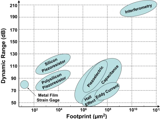
Figure 1.9 [1.40] plots the dynamic range of each sensor technology against the sensor’s footprint. Interferometers are impractical for use in next generation MDOF nanopositioning stages because the cost of the metrology system would be orders of magnitude larger than the cost of the nanopositioner itself. The inability of piezoelectric sensors to reliably measure a static position makes them impractical for MDOF nanopositioners. Capacitive sensors require too large a footprint to be integrated into meso-scale nanopositioners. Hall effect and eddy current sensors are difficult to implement into small-scale MDOF nanopositioners because of their sensitivity to electromagnetic interference and the difficulty in closed-form modeling magnetic fields. Piezoresistive strain sensors offer the best balance of range and resolution, environmental disturbance rejection, and relative footprint. Figure 1.9 shows that piezoresistive strain sensors also have the largest dynamic range for the smallest footprint. These benefits come at a cost of indirect measurement of the displacement of the positioning stage and the need to mitigate thermal sensitivity of the piezoresistive material. Since these effects can be mitigated through careful engineering and proper design, piezoresistive sensors are the best choice.
50 70 102 Pie zoel ectr ic Interfero metry Eddy Curren t 90 110 130 150 170 190 210 104 Silico n Piezor esisto r Metal Film Strain Gage Polys ilicon Piezo resist or 106 108 1010 1012
Footprint (µm
2)
D
y
n
a
m
ic
R
a
n
g
e
(
d
B
)
Hall Effec t Cap acita nceFigure 1.9: Dynamic range versus characteristic footprint for different sensing technologies.
1.2.2 Flexural Mechanism Design Tools
The integration of strain-based sensors inherently couples the metrology subsystem to the mechanical subsystem because the change in resistance of the strain sensor has a linear dependence on the strain in the sensed beam. It is important that current concept synthesis and design tools for flexural mechanisms take into account the addition of the metrology subsystem because of the coupled nature of this design problem. The following subsections will outline the major design tools currently used for flexure synthesis. It will also discuss how the metrology subsystem is accounted for in these design tools.
1.2.2.1 Topology Synthesis
Topological synthesis [1.59-1.61] tools design a flexural mechanism via computer iteration of design parameters that are subject to an objective function. In topological synthesis a design domain, shown in Fig. 1.10(a), is broken into a series of nodes and beam elements.
(a) (b)
Figure 1.10: Design domain for topological synthesis and resulting topology after computer iteration.
Global displacements and forces are applied to the design domain and a computer iteratively removes and adds nodes and beam elements until a suitable flexural mechanism has been synthesized. This process is illustrated in Fig. 1.10(b). After removing and adding nodes and beam elements, the result is tested via finite element analysis (FEA) to ascertain its performance. When the main topology of a flexural mechanism is found, the computer then varies parameters of the beams such as length, material properties, and moment of inertia in order to optimize performance criteria such as mechanical advantage, material weight/cost, stored energy, and fatigue/failure.
Although work on the optimization of flexure topologies with embedded strain sensing has been conducted [1.62], there are significant limitations to the current technology and design knowledge. The current method maximizes an objective function containing a number of weighted constraints. Prescribing the relative value of these weights in a non-arbitrary way is difficult and there is no clear method for how to assign relative weights for large numbers of functional requirements. The preceding makes it difficult to guarantee that the desired mechanical and sensing performance will be achieved. Hard constraints, such as a minimum sensed resolution, tend to become binary constraints when used by the genetic algorithm for maximizing the objective function. This makes it difficult and time consuming (~weeks of computation [1.62]) to optimize the topology of a particular concept.
Topology synthesis separately maximizes the mechanical dynamic range and sensor dynamic range for a particular concept. There is no guarantee that these dynamic ranges will coincide, and so system performance is not necessarily maximized for concepts with a maximized

![Figure 2.11: Hooge constant for silicon as a function of anneal temperature. Data taken from Vandamme et al [2.34]](https://thumb-eu.123doks.com/thumbv2/123doknet/14448099.518128/78.918.222.709.113.395/figure-hooge-constant-silicon-function-anneal-temperature-vandamme.webp)