HAL Id: hal-01323323
https://hal.archives-ouvertes.fr/hal-01323323
Submitted on 30 Jun 2016HAL is a multi-disciplinary open access
archive for the deposit and dissemination of sci-entific research documents, whether they are pub-lished or not. The documents may come from teaching and research institutions in France or abroad, or from public or private research centers.
L’archive ouverte pluridisciplinaire HAL, est destinée au dépôt et à la diffusion de documents scientifiques de niveau recherche, publiés ou non, émanant des établissements d’enseignement et de recherche français ou étrangers, des laboratoires publics ou privés.
Thin films sputtered from Ba2NdFeNb4O15 multiferroic
targets on BaFe12O19 coated substrates
Romain Bodeux, Dominique Michau, Mario Maglione, Michaël Josse
To cite this version:
Romain Bodeux, Dominique Michau, Mario Maglione, Michaël Josse. Thin films sputtered from Ba2NdFeNb4O15 multiferroic targets on BaFe12O19 coated substrates. Materials Research Bulletin, Elsevier, 2016, 81, pp.49-54. �10.1016/j.materresbull.2016.04.027�. �hal-01323323�
Thin films sputtered from Ba
2NdFeNb
4O
15multiferroic
1targets on BaFe
12O
19coated substrates
23
Romain Bodeux, Dominique Michau*, Mario Maglione and Michaël Josse 4
5
6
ICMCB-CNRS, Université de Bordeaux, 87 avenue du Dr. A. Schweitzer, Pessac F-33608, 7
France 8
9
10
* Author to whom correspondence should be addressed. Electronic mail: 11 [email protected] 12 13 14 15 16 17 18
Abstract
1
2
Ba2NdFeNb4O15 tetragonal tungsten bronze (TTB) / BaFe12O19 (BaM) hexaferrite bilayers
3
have been grown by RF magnetron sputtering on Pt/TiO2/SiO2/Si (PtS) substrates. The BaM
4
layer is textured along (00l) while the TTB layer is multioriented regardless of the PtS or 5
BaM/PtS substrate. Dielectric properties of TTB films are similar to those of bulk, i.e., ~ 6
150 and a magnetic hysteresis loop is obtained from TTB/BaM bilayers, thanks to the BaM 7
component. This demonstrates the possibility of transferring to 2 dimensional structures the 8
composite multiferroic system TTB/BaM previously identified in 3 dimensional bulk 9
ceramics. 10
11
12
KEYWORDS: A. magnetic materials, A. multilayers, B. sputtering, C. impedance 13
spectroscopy, D. multiferroics 14
1) Introduction
1
2
“The world Multiferroic” was coined for materials in which ferroic orders, i.e. ferroelectricity 3
(FE), ferromagnetism (FM), ferroelasticity,… coexist in the same phase. These 4
multifunctional materials have recently attracted great scientific and technologic interests due 5
to their versatile properties which could lead to potential applications in memory devices, 6
actuator and sensors [1]. Multiferroism can be achieved when, in a single-phased material, 7
one cationic sublattice induces a structural distortion and a polarization, while a second 8
sublattice built of paramagnetic ion induces a magnetization[2]. However such materials are 9
relatively unusual and many efforts have been dedicated to “multiferroic composite 10
materials”, which associate two ferroic phases [3]. Commercial magnetoplumbite type barium 11
ferrite BaFe12O19 (BaM) is a good candidate for the design of multiferroic composites because
12
it is a hard magnet, with a large uniaxial anisotropy which could be useful in micro- or 13
nanostructured materials. Different devices were recently investigated combining BaM with a 14
ferroelectric material, i.e. SrBa2Ta2O9/BaM thin films heterostructures [4], multilayers
15
consisting of alternating BaM layers with Pb(Zr,Ti)O3 (PZT) [5] or (Ba,Sr)TiO3 (BST)
16
perovskite layers [6-11] and self-assembled BaM clusters embedded in a PZT or BST matrix 17
[12-14]. It was also shown that BaTiO3/BaM ceramics exhibit magnetoelectric coupling at
18
room temperature [15,16]. 19
The main aim of the present paper is to show that tetragonal tungsten bronze niobiates can be 20
alternative compounds for the processing of such composite multiferroics. TTB forms an 21
important family of dielectric materials. Their general formula (A1)4(A2)2(C)4(B1)2(B2)8O30
22
allows many cationic substitution that leads to tunability in their physical properties. Thus 23
TTB could be easily compatible with coexistance of ferroelectricity and ferromagnetism after 24
the introduction of paramagnetic cations. Original bulk multiferroics composites were already 25
identified in the Ba2LnFeNb4O15 (Ln:TTB) family (Ln = Nd, Sm and Eu) [17,18].
1
Ferroelectric behaviour in this family is driven by the size of the rare earth ions and their 2
accommodation leads to the formation of a small amount of barium ferrite BaM. This 3
magnetic phase is generated in situ during the ceramic processing, which indicates a very high 4
chemical stability of both FE and FM phases in this composite system. Castel and al. 5
investigated the elaboration of Eu:TTB composite samples with an excess of hematite in the 6
nominal composition [19], while Roulland et al. tuned the Europium content in Eu:TTB [20]. 7
They have shown that the magnetic response is modulated by the amount barium ferrite, 8
which can be increased with excess of hematite or reduced by diminishing the rare earth 9
content. More recently, Ta substitution for Nb was identified as another crystal chemical lever 10
to control these multiferroic composites [21]. Attempts to induce the formation of barium 11
ferrite in other TTB structured system proved unsuccessful, revealing how special the 12
Ba2LnFeNb4O15 composite multiferroic ceramics are rare [22]. Thus multiferroic composites
13
based on these TTBs, in which ferroelectric properties and magnetization can be tuned, are of 14
interest. In this view, it is important to investigate Ln:TTB thin film deposited on BaM 15
coated substrate. Stability and chemical compatibility of BaM with Ln:TTB is a real 16
advantage for this heterostructure, although it seems particularly complex and requires 17
optimum growth for both TTB and BaM layers. Previous reports on individual BaM and TTB 18
films are encouraging for the development of such systems,. On the one hand, BaM thin films 19
deposited on PtS were widely studied because a Pt underlayer favors the growth along the 20
easy axis of magnetization, required for applications [23,24]. On the other hand, relaxor TTB 21
thin films were deposited by RF magnetron sputtering on Pt(111) and showed dielectric 22
properties very close to those of bulk ceramics [25,26]. 23
In the present work, we compare growth orientation, microstructure and dielectric properties 24
of Ba2NdFeNb4O15 films deposited on silicon with Pt or BaM/Pt intermediate layers. We find
that the ferromagnetic properties of BaM and the intrinsic TTB dielectric behaviour are kept 1
in such bi-layers. More interestingly, because of the good chemical and structural 2
compatibility between the two phases, possible magneto-dielectric coupling is anticipated. 3
4
2) Experiments
5
6
Ba2NdFeNb4O15 tetragonal tungsten bronze (TTB) and BaFe12O19 (BaM) ceramic targets were
7
prepared through a solid state route. TTB target was sintered at 1300°C from stoichiometric 8
mixture of BaCO3, Fe2O3, Nb2O5 and Nd2O3 [25] while BaM was sintered at 1000°C from
9
stoichiometric mixture of BaCO3 and Fe2O3. The purity of the targets was checked by XRD
10
using small control pellets sintered with the targets. 11
TTB films were grown on Pt(111)/TiO2/SiO2/Si(100) (PtS) and BaM/PtS substrates by RF
12
magnetron sputtering (Plassys PM450 - 13.56 MHz) [19]. During all depositions, the 13
atmosphere pressure of 40 mTorr was a mixture of 10% O2 and 90% Ar. PtS substrates were
14
purchased from INOSTEK and appropriate masking during the films deposition enabled the 15
use of the Pt underlayer as the bottom electrode. The deposition parameters of BaM films 16
were optimized regarding crystalline quality and following previous reports [23,24]. All BaM 17
films were deposited at 300 °C. Crystallization took place in a tubular furnace during the post 18
deposition annealing step at 850°C for 3 H in oxygen atmosphere. TTB films were deposited 19
at 300 °C and post annealed at 800°C for 1 H in oxygen atmosphere. Films thickness was 20
measured using a Veeco Dektak6M stylus profile mechanical profilometer. Various 21
thicknesses of layer were obtained by appropriately tuning the deposition time, the thickness 22
of TTB layers varying between 250 nm and 1000 nm, that of BaM layers one varying 23
between 0 and 200 nm (table 1). X-ray diffraction data in the –2 Bragg–Brentano 24
geometry were recorded on a Philips XPert pro diffractometer (Cu K1 radiation, = 1.54056
Å) with 10° < 2< 80° and step = 0.02°. Sample’s surface morphology was examined by 1
atomic force microscopy (Veeco dimension 3100). Magnetic hysteresis loops were measured 2
on a SQUID magnetometer (MPMS, Quantum Design Inc.) on samples cut to small pieces 3
compatible witht the sample holder. Pt Circular dots were deposited ex-situ at room 4
temperature as a top electrode by dc sputtering through a metal mask at room temperature. 5
The dot geometry defined the capacitors area: S = 0.1 mm2. Dielectric properties of capacitors
6
were measured in the metal/insulator/metal configuration using a Hewlett-Packard 4194 7
impedance analyser as a function of frequency (100 Hz – 1 MHz) and temperature (on 8
heating) with an ac excitation amplitude of 100 mV. 9
10
3) Results and discussion
11
12
After standard solid state processing of powders and dense ceramics, X-ray diffraction (XRD) 13
evidenced the successful stabilisation of the tetragonal tungsten bronze structure for the 14
compound Ba2NdFeNb4O15 (TTB). The XRD pattern of the TTB ceramic target is shown in
15
Fig.1a. Diffraction pattern matches with the reference data for homologous Ba2LaNb5O15
16
TTB (JCPDS 46-0232). In a previous work [27], X-ray microprobe experiment revealed that 17
traces of BaFe12O19 (BaM) barium ferrite should be present in the target ceramics, although it
18
was not detected by XRD. In fact, chemical strain and distortions induced by smaller rare 19
earths lead to the evolution of the TTB compositions and the occurrence of secondary phases, 20
i.e. LnNbO4 fergusonite and BaM.
21
Fig. 1b shows the XRD pattern of a sputtered films deposited at 300°C and of a film post-22
annealed at 800°C (sample A in table 1). After deposition the films were amorphous and post-23
annealing was required to trigger crystallisation. The annealed films displayed a diffraction 24
pattern compatible with the TTB structure, with several peaks easily identified by comparison 25
with the ceramic target. The films were polycrystalline and the diffraction peaks exhibited a 1
distribution of relative intensity rather similar to that of ceramics. A notable exception to 2
these intensity ratio is found with (00l) peaks, the amplitude of which is significantly larger 3
than in the ceramics. This suggests a partial texturation of the polycrystalline film along [001] 4
. The overall multioriented growth of films is nonetheless in agreement with other post-5
annealed compounds of the same family [28]. The mismatch of peak positions with those of 6
ceramic indicates that the films are compressive strained. Strain can be induced by the lattice 7
misfits between TTB and Pt at the interface or produced by the intrinsic stress during the post-8
annealing. The diffraction peaks, which are relatively narrow, suggest a good quality of the 9
films. The full width at half maximum (FWHM) of TTB(001) reflection is 2 = 0.19° which 10
is close to that of Pt(111) which is 2 = 0.20°. An average crystallite size of about 50 nm 11
was obtained by the Scherrer’s formula. 12
The use of BaFe12O19 (BaM) for high density magnetic recording applications requires thin
13
films with perpendicular c-axis orientation, because of BaM large magnetic anisotropy. C-14
axis growth of BaM can be obtained by using a Pt underlayer [23,29-33]. However, high 15
temperature deposition is required to produce BaM films with high quality by RF magnetron 16
sputtering and post annealing was generally undertaken [24]. Our preliminary works are in 17
agreement with these previous reports. XRD pattern are shown in Fig. 2 for the BaM films 18
deposited on PtS(111) with optimized conditions (sample C) in table 1. The BaM films 19
displayed intense (00l) peaks, indicating that the films are crystallized and suggesting a (00l) 20
texture. From the crystallography view point, the (111) plane of packed Pt atoms is seen as a 21
hexagonal structure with a lattice constant a = 5.547 Å, which is close enough from (001) 22
plane of the hexagonal BaM structure with a = 5.892 Å. The relatively small mismatch 23
between Pt(111) and BaM(001) favors the c-axis orientation of the BaM layer. The TTB films 24
were deposited on BaM/PtS in the same deposition conditions than the ones on PtS, i.e. as-25
deposited TTB films were amorphous and crystallization took place during the post 1
deposition annealing step at 800 °C (sample E). Fig.2 shows XRD pattern for the 2
TTB/BaM/PtS stack (sample E). TTB films are multioriented while BaM remains textured 3
(001), and this results demonstrates the successful deposition of TTB on the BaM phase to 4
form a bilayer. The peaks of the BaM layer are well defined indicating that the integrity of the 5
BaM phase was preserved through the second heat treatment. More interesting, the 6
introduction of a BaM buffer layer restores the random orientation of the grains in the TTB 7
film. Generally, when synthesizing bi- or multilayers, the structure is significantly affected by 8
the under-layer structure. The under-layer can lead to strains of the top layer crystal lattice 9
and partial texturing. However, the large mismatch of both Pt and BaM with the tetragonal 10
structure of TTB layer (a ~ 12.48 Å in the ceramic) should induce disorder and dislocations at 11
the interface. The interaction between BaM/Pt and TTB confines at the interface. Thus, the 12
structure within TTB layer remains unchanged and random orientations of grains take place. 13
Furthermore growth procedure can play a significant role on the TTB structure. In fact, we 14
observed similar results on ceramic composites, which are obtained from solid state route 15
consisting in a mixture followed by sintering at highest temperature ~1200°C, i.e. both TTB 16
and BaM phases were maintained. This shows that these two phases coexist without any 17
intermixing in these thermodynamical conditions. 18
Fig. 3a and Fig 3b show the typical morphology of the surface for TTB films deposited on PtS 19
and BaM/PtS substrates (sample A and sample E, respectively). The grains are distinctly 20
visible, assuming that the films are well crystallized, as confirmed by XRD. The grains are 21
densely and regularly packed without cracks or voids and the surfaces are relatively uniform 22
and smooth. The film shows a granular surface with a regular and fine grain size about 50 nm 23
which is comparable to the crystallite size obtained from XRD data. The granular surface of 24
films is typical of post-annealed films formed from amorphous film precursors. It was also 25
observed in others materials [34] and is relatively independent of the buffer layer [35,36]. The 1
root-mean-square (rms) roughness surface roughness is about 4.4 nm and 7.6 nm for PtS and 2
BaM/PtS substrates. The higher value for BaM/PtS has to be associated with the roughness of 3
BaM (about 13.3 nm) which leads to dark areas on the picture obtained from TTB/BaM/PtS 4
stacks. However, the peak-valley distance (50 nm) is clearly lower than the thickness of all 5
TTB films (>250 nm). Therefore, the TTB films are suitable for dielectric measurements in 6
metal/insulator/metal configuration. 7
Ferromagnetic response of Ba2NdFeNb4O15 ceramics is related to the presence of
8
small amount of barium ferrite and this spontaneous magnetization reaches MS ~ 1 emu/g at
9
10 kOe [27]. The smaller quantity of matter in the films (three orders of magnitude with 10
respect to ceramics), would yield traces of in situ formed BaM, which should not be sufficient 11
to overcome the diamagnetic response of PtS substrate, i.e. Mdia ~ 2 memu per gram of PtS
12
substrate at 10 kOe (not shown). However, the magnetic properties of TTB composites can be 13
controlled by inducing the formation of an excess of barium ferrite [19]. In this view, the 14
elaboration of TTB/BaM/PtS stacks should allow to investigate a layered architecture, which 15
could be used as a model system of the corresponding ceramic system. Magnetic hysteresis 16
loops of such a stack (sample E) at 300 K are shown in Fig. 4. The stack exhibits large 17
remanence, as expected for a single BaM layer. The loop is attributed to the prevailing easy-18
axis of magnetization along the BaM(001) orientation [23]. Spontaneous magnetization 19
reaches ~7.10-3 emu per gram of PtS substrate while the coercive field is about 1 kOe, which
20
is consistent with the values reported for BaM films [37]. 21
The capacitance C was extracted from impedance measurements Z* Z’-jZ’’. The dielectric 22
losses were related to the complex impedance through the relation tan = Z’/Z’’. In figure 5 23
is shown the frequency dependence of capacitance and the dielectric losses for the 24
TTB/BaM/PtS stacks with various thicknesses of BaM layer, 0, 100 et 200 nm (sample A, E 25
and B, respectively). Below 10 kHz, capacitance exhibits a constant value about 5 nF/mm2 for
1
the stack with a BaM layer thickness of 100 nm, similar to the one observed in a TTB single 2
layer. The capacitance slightly decreases about 3.5 nF/mm2 when the BaM layer thickness
3
increases, as discussed below. Thus, the dielectric properties of TTB films are maintained 4
when deposited on the BaM buffer layer. These results are consistent with the XRD and AFM 5
measurements which show that the TTB layer is not affected by the BaM layer. To values 6
greated than 10 kHz, a decrease of capacitance is observed for the TTB/BaM/PtS stack. The 7
relaxation in capacitance is accompanied by a broad peak in tan at f = 300 kHz, which doe 8
not appear in the TTB/PtS stack. For the TTB/PtS stack, the limited increase of dielectric 9
losses at 1 MHz is an artefact arising from the stray inductance of the contacts. The 10
appearance of a dielectric anomaly on TTB/BaM/PtS stacks suggests that it is related to the 11
insertion of the BaM layer. BaM is extensively used in the microwaves devices because of its 12
high resistivity which allows minimizing the losses. This dielectric response of the BaM layer 13
may act as an additional impedance source on the impedance measurements connected in 14
series to the TTB film [36]. From these results, the dielectric response can be modelled and 15
analysed using two RC parallel electrical elements, one corresponding to TTB film and the 16
others to an interface capacitance. The contribution of each of these elements to the dielectric 17
response is then visible over characteristic frequency ranges, i.e. = (RC)-1. Thus, the
18
dielectric response of the TTB layer dominates at low frequency while that of the BaM layer 19
appears at high frequency. 20
To further analyse the size effect in stacks, the dielectric properties of four TTB/BaM 21
stacks were studied for which the TTB layer were deposited at various thicknesses: 250, 500, 22
750 and 1000 nm (sample D, E, F and G, respectively). The frequency dependence of 23
capacitance and tanare shown in Fig. 6a and 6b, respectively. The capacitance slightly 24
increases from 2.1 nF/mm2 to 4.8 nF/mm2 when the thickness of the TTB layer decreases for
1
the high frequency range f < 100 kHz, 2
A large increase of capacitance is observed when the frequency decreases below 100 kHz, 3
especially for the 250 nm TTB layer. It is accompanied by a large relaxation in tan The 4
largest capacitance is associated with the thinner TTB layer. In this analysis, the stack 5
capacitance Cstack can be written as
6
7
[1] 8
9
where CTTB, CBaM, TTB, BaM, tTTB and tBaM denotes the capacitances, the permittivity and the
10
thickness of the TTB and BaM layers, respectively. By plotting 1/Cstack vs tTTB and tBaM curves
11
at low frequency, f = 100 Hz, and high frequency, f = 1 MHz, from the inset figures 5 and 6, 12
we determine from their slopes the experimental values of TTB ~ 150 and BaM ~ 40 which are
13
consistent with ones reported in the literature [26,38] 14
Capacitance and losses of a Pt/TTB/BaM/PtS stack (sample G) are plotted as a 15
function of the temperature at various frequencies 10 kHz, 100 kHz and 1 MHz in Fig. 7. 16
Capacitance exhibits a steplike feature from a low-temperature plateau value of 1.6 nF/mm2
17
towards 2.5 nF/mm2 at high temperatures. The step shifts to higher temperatures with
18
increasing frequency. This typical signature is commonly reported as a Maxwell Wagner 19
relaxation [39]. This relaxation is caused by the contribution of two different electrical 20
elements evidenced in Figure 5 and 6, such as the TTB layer capacitance visible at high 21
temperature and low frequency and the BaM layer capacitance observed at low temperature 22
and high frequency. In addition, the step in C(T) is transferred into a peak in tan (T). The 23
characteristic frequency (fr) of this relaxation is governed by the resistance and capacitance of
24
both TTB and BaM layers according to the relation [39] 25 S BaM BaM t S TTB TTB t BaM C TTB C stack C 1 1 1
[2] 1
2 3
From Fig. 6 and Fig. 7, it appears that on the one hand RTTB and RBaM, and on the other hand
4
CTTB, and CBaM are the same order of magnitude and therefore each term contributes
5
significantly to the relaxation. The peak shifts to the highest temperatures as the frequency is 6
increased. The relaxation frequency was fitted with an Arrhenius law with a characteristic 7
activation energy Ea ~ 0.34 eV. In hexaferrites, the conductivity arises mainly with
8
temperature from electron hopping between Fe3+ and Fe2+ cations. caused by the presence of
9
oxygen vacancies. The activation energy of this mechanism is about 0.3 eV and could explain 10
the relaxation observed in our TTB/BaM stacks [40]. For a TTB single layer, a
low-11
temperature anomaly was also observed and was likely related to a relaxor behaviour [24]. A similar
12
value of activation energy of 0.3 eV was reported although the anomaly is shifted to lower
13
temperatures with respect to the Maxwell-Wagner relaxation observed in the stacks. Both mechanisms
14
are rather different, but one should keep in mind that Fe3+ cations are also present in TTB compound.
15
Moreover in TTB single crystals, Fe0, 2+, 3+ ions were detected from XPS spectra and were associated
16
with reduced niobium ions (Nb5+, 4+, 3+). Significant dielectric losses were clearly seen in these crystals
17
and may be related to electron hopping within the octahedral framework, as it is statistically occupied
18
by iron and nobiumions. [18]. Further investigation is needed to assess the mechanisms involved both
19
in TTB single layers and in TTB/BaM stacks. Anyhow, the results presented here demonstrate a good
20
potential for the coexistence of ferroelectricity and ferromagnetism in TTB/BaM bilayer thin films.
21
We plan to improve their quality by different synthesis route in order to look for a
magneto-22 capacitance effect. 23 24 4) Conclusion 25 26
Tetragonal tungsten bronze and barium ferrite films from Ba2NdFeNb4O15 (TTB) and
1
BaFe12O19 (BaM) homemade ceramic targets were obtained by RF magnetron sputtering on Pt
2
and postannealed. It was found that growth orientation, microstructure and dielectric 3
properties of the TTB layer were retained regardless of the underlayer (Pt bottom electrode or 4
BaM). A dielectric relaxation appears on Pt/TTB/BaM/PtS stacks and suggests that the 5
insertion of the BaM layer provides an additional impedance source. The capacitance of the 6
TTB layer is visible at high temperature and low frequency whereas that of BaM layer is 7
observed at low temperature and high frequency. The relaxation frequency follows an 8
Arrhenius relationship with a characteristic activation energy Ea ~ 0.34 eV, and is likely
9
related to a Maxwell-Wagner effect. Magnetic hysteresis loops were obtained from the stacks, 10
and are consistent with the magnetic properties of the BaM layer. The loop is attributed to the 11
prevailing easy-axis of magnetization along the BaM(001) orientation. This allows for further 12
development of TTB/BaM/PtS bilayers and multilayers as multiferroic and possibly 13 magnetoelectric composites. 14 15 Acknowledgments 16 17
This project was supported by the French Agency for Research under contract ANR 18
CROCRODIEL(Grant ANR-09-JCJC-0079). 19
Reference
1
2
[1] L.W. Martin, Y. –H. Chu and R. Ramesh, Mater. Sci. and Eng. R 68 (2010) 89. 3
[2] A. M. dos Santos, S. Parashar, A. R. Raju, Y. S. Zhao, A. K. Cheetham and C. N. Rao, 4
Solid State Commun. 122 (2002) 49. 5
[3] C-W Nan, M.I. Bichurin, Shuxiang Dong, D. Viehland and Srinivasan, J. Appl. Phys. 103 6
(2008) 031101. 7
[4] D. Chen, I. Harward, K. Linderman, E. Economou, Y. Nie, and Z. Celinski, J. Appl. Phys. 8
115 (2014) 17D713 9
[5] G. Srinivasan, I. V. Zavislyak and A. S. Tatarenko, Appl. Phys. Lett. 89 (2006) 152508. 10
[6] N.A. Frey, R. Heindl, S. Srinath, H. Srikanth, N.J. and Dudney, Mater. Res. Bull. 40 11
(2005) 1286. 12
[7] S. Srinath, N. A. Frey, R. Heindl, H. Srikanth, K. R. Coffey and N. J. Dudney, J. Appl. 13
Phys. 97 (2005) 10J115 14
[8] R. Heindl, H. Srikanth, S. Witanachchi, P. Mukherjee, A. Heim, G. Matthews, S. 15
Balachandran, S. Natarajan and T. Weller, Appl. Phys. Lett. 90 (2007) 252507. 16
[9] R. Heindl, H. Srikanth, S. Witanachchi, P. Mukherjee, T. Weller, A. S. Tatarenko and G. 17
Srinivasan, Appl. Phys. Lett. 101 (2007) 09M503 18
[10] Y.-Y. Song, J. Das, P. Krivosik, N. Mo and C.E. Patton, Appl. Phys. Lett. 94 (2009) 19
182505. 20
[11] J. Das, Y.-Y. Song and M. Wu, J. Appl. Phys. 108 (2010) 043911. 21
[12] R. Hajndl, J. Sanders, and H. Srikanth, J. Appl. Phys. 93 (2003) 7999. 22
[13] D. V. Karpinsky, R. C. Pullar, Y. K. Fetisov, K. E. Kamentsev and A. L. Kholkin J. 23
Appl. Phys. 108 (2010) 042012. 24
[14] J. D. S. Guerra, Madhuparna Pal, R. J. Portugal, L. F. Cótica, I. A. Santos, R. Guo, and 1
A. S. Bhalla, J. Appl. Phys. 114 (2013) 224113 2
[15] A. Srinivas, R. Gopalan and V. Chandrasekharan, Solid State Commun. 149 (2009) 367 3
[16] H. Trivedi,V.V. Shvartsman, D.C. Lupascu, M.S. A. Medeiros, R.C. Pullar, A.L. 4
Kholkin, P. Zelenovskiy, A. Sosnovskikhd and V. Y. Shurd, Nanoscale 7 (2015) 4489 5
[17] E. Castel, P. Veber, M. Albino, M. Velazquez, S. Pechev, D. Denux,J.P. Chaminade, M. 6
Maglione ,M. Josse, J. Cryst. Growth 340 (2012) 156 7
[18] M. Albino, P. Veber, S. Pechev, C. Labrugère, M. Velazquez, M. Maglione and M. 8
Josse, Cryst. Growth Des., 14 (2014) 500 9
[19] E. Castel, M. Josse , F. Roulland, D. Michau, L. Raison and M. Maglione, J. Magn 10
Magn. Mater. 321 (2009) 1773. 11
[20] F. Roulland, M. Josse, E. Castel and M. Maglione, Solid State Sci. 11 (2009) 1709. 12
[21] E. Castel, M. Maglione, M. Josse, submitted to Solid State Sci. 13
[22] M. Josse, P. Heijboer, M. Albino, F. Molinari, F. Porcher, R. Decourt, D. Michau, S. 14
Pechev, P. Veber, M. Velazquez, M. Maglione, Cryst. Growth Des., 2014, 14(11), 5428-5435 15
[23] X. Sui, B.-K. Cheong, D. E. Laughlin and M. H. Kryder, J. Magn. Soc. Jpn 18-S1 (1994) 16
319. 17
[24] A. Morisako, T. Naka, K. Ito, A. Takizawa, M. Matsumoto and Y.-K. Hong, J. Magn 18
Magn. Mater. 242 (2002) 304. 19
[25] Michau et A. Simon et M. Maglione, J. Phys. D 42(7), (2009) 075407 20
[26] R. Bodeux, D. Michau, M. Josse and M. Maglione, Solid State Sci., 38 (2014) 112. 21
[27] M. Josse, O. Bidault, F. Roulland, E. Castel, A. Simon, D. Michau, R. Von der Mühll, O. 22
Nguyen and M. Maglione Solid State Sci. 11 (2009) 1118. 23
[28] S.-K. Park, M.-S. Baek, S.-C. Bae, S.-Y. Kwon, J.-H. Kim and Ki-W. Kim, Solid State 24
Commun. 111 (1999) 125 25
[29] X. Sui, M. Scherge, M.H. Kryder, J.E. Snyder, V.G. Harris and N.C. Koon, J. Magn 1
Magn. Mater. 155 (1996) 132. 2
[30] Z. Zhuang, M. Rao, D. E. Laughlin and M.H. Kryder, J. Appl. Phys. 85 (1999) 6142. 3
[31] Z. Zhuang, M.Rao, R. M. White, David E. Laughlin and Mark H. Kryder, J. Appl. Phys. 4
87 (2000) 6370.
5
[32] N.N. Shams, X. Liu, M. Matsumoto and A. Morisako, J. Magn Magn. Mater. 290 6
(2005) 138. 7
[33] Q. F. Li, X. D. Su, H. Li, L. Zhang, Z. H. Liu and H. J. Zhong, J. Appl. Phys. 106 (2009) 8
123914. 9
[34] R. Singh, T.C. Goel and S. Chandra, Mater. Res. Bull. 43 (2008) 384. 10
[35] W. Leng, C. R. Yang, J. H. Zhang, H. W. Chen, H. Ji, C. L. Fu and J. X. Liao, J. Appl. 11
Phys. 99 (2006) 114904. 12
[36] W. Leng, C. Yang, H. Ji, J. Zhang, J. Tang, H. Chen and L. Gao, J. Phys. D 40 (2007) 13
1206. 14
[37] M. Matsuoka, M. Naoe and Y. Hoshi, J. Appl. Phys. 57 (1985) 4040. 15
[38] R.M. Almeida , W. Paraguassu, D.S. Pires, R.R. Corrêa and C.W. de Araujo Paschoal, 16
Ceram. Int. 35 (2009) 2443. 17
[39] R. Bodeux, M. Gervais, J. Wolfman, C. Autret-Lambert, G. Liu and F. Gervais, Thin 18
Solid Films, 520 (2012) 2632. 19
[40] M. Manikandan and C. Venkatesswaran, J. Magn Magn. Mater. 358 (2014) 82. 20
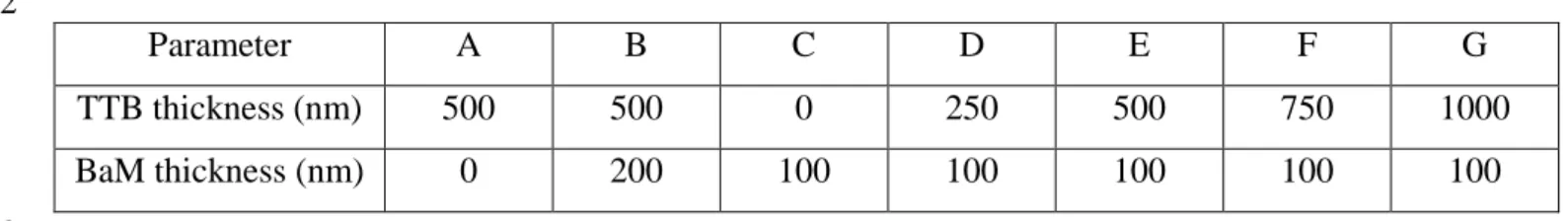
Table 1Thickness of TTB and BaM layers for TTB/BaM/PtS stacks 1 2 Parameter A B C D E F G TTB thickness (nm) 500 500 0 250 500 750 1000 BaM thickness (nm) 0 200 100 100 100 100 100 3
Fig1. XRD patterns for a) the TTB ceramic target and b) as deposited TTB/PtS film and 1
annealed TTB/PtS film (sample A) 2
3
Fig.2 XRD patterns for BaM/PtS film (sample C) and TTB/BaM/PtS (sample E) 4
5
Fig. 3 (Color online) Morphology image (AFM) of TTB films deposited on a) PtS (sample A) 6
and b) BaM/PtS (sample E) 7
8
Fig. 4 Magnetization per gram of PtS substrate for the TTB/BaM/PtS stack. Thickness of the 9
BaM layer is 100 nm (sample E). 10
11
Fig. 5 Frequency dependence of a) capacitance and (b) the dielectric losses for the 12
Pt/TTB/BaM/PtS with BaM thickness of 0 nm (sample A), 100 nm (sample E) and 200 nm 13
(sample B) 14
15
Fig. 6 Frequency dependence of (a) the capacitance and (b) the dielectric losses for the 16
Pt/TTB/BaM/PtS capacitors with various TTB thicknesses 250 nm (sample D), 500 nm 17
(sample E), 750 nm (sample F) and 1000 nm (sample G) 18
19
Fig. 7 Temperature dependence of a) the capacitance and b) dielectric loss for the 20
Pt/TTB/BaM/PtS (sample G) for various frequency 10 kHz, 100 kHz and 1 MHz 21