HAL Id: hal-02001631
https://hal.archives-ouvertes.fr/hal-02001631
Submitted on 31 Jan 2019
HAL is a multi-disciplinary open access
archive for the deposit and dissemination of
sci-entific research documents, whether they are
pub-lished or not. The documents may come from
teaching and research institutions in France or
abroad, or from public or private research centers.
L’archive ouverte pluridisciplinaire HAL, est
destinée au dépôt et à la diffusion de documents
scientifiques de niveau recherche, publiés ou non,
émanant des établissements d’enseignement et de
recherche français ou étrangers, des laboratoires
publics ou privés.
Towards a mixed NoC/AFDX architecture for avionics
applications
Laure Abdallah, Jérôme Ermont, Jean-Luc Scharbarg, Christian Fraboul
To cite this version:
Laure Abdallah, Jérôme Ermont, Jean-Luc Scharbarg, Christian Fraboul.
Towards a mixed
NoC/AFDX architecture for avionics applications. 13th International Workshop on Factory
Commu-nication Systems (WFCS), May 2017, Trondheim, Norway. pp.1-10, �10.1109/WFCS.2017.7991950�.
�hal-02001631�
OATAO is an open access repository that collects the work of Toulouse
researchers and makes it freely available over the web where possible
Any correspondence concerning this service should be sent
to the repository administrator:
[email protected]
This is an author’s version published in:
http://oatao.univ-toulouse.fr/21539
To cite this version:
Abdallah, Laure and Ermont, Jérôme and Scharbarg,
Jean-Luc and Fraboul, Christian Towards a mixed NoC/AFDX
architecture for avionics applications. (2018) In: 13th
International Workshop on Factory Communication Systems
(WFCS), 31 May 2017 - 2 June 2017 (Trondheim, Norway)
Official URL:
https://doi.org/10.1109/WFCS.2017.7991950
Towards a mixed NoC/AFDX architecture for
avionics applications
Laure Abdallah, J´
erˆ
ome Ermont, Jean-luc Scharbarg and Christian Fraboul
IRIT INP-ENSEEIHT, Universit´e de ToulouseF-31000 Toulouse, France Email: [email protected]
Abstract—An heterogeneous network, where a switched-Ethernet backbone, as AFDX, interconnects
several End Systems based on Network-On-Chip
(NoC), is a promising candidate to build new avionics architecture. However, current avionics End System includes many functions, as performing a traffic shaping for each Virtual Link (VL) and scheduling the output frames in such a way the jitter on each VL is bounded. This paper describes how the NoC implements these functions in order to compute the worst-case traversal time (WCTT) of avionics frames on a NoC to reach the AFDX network. Besides, we illustrate the problem of guaranteeing a bounded jitter at the output of a NoC. We show that the existing mapping strategies present some limitations to reduce the congestion on the outgoing I/O flows (i.e. going from the NoC to the AFDX network) and so do not reduce the jitter on a given VL. We propose an extended mapping approach which considers the outgoing I/O flows. Experimental results on realistic avionics case studies show significant improvements of the jitter value.
I. Introduction
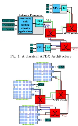
Avionics systems evolved from a federated architecture to a distributed one in order to deal with the increase of the avionics functions. In a federated architecture, each func-tion is executed by a dedicated computer. The distributed architecture is based on the Integrated Modular Avionics (IMA) concept. As depicted in Figure 1, the architecture is composed of a set of computer systems typically inter-connected by an Avionics Full Duplex switched Ethernet network (AFDX). Each computer is shared by a set of avionics functions accessing the sensors and the actuators and exchanging data with other functions. Data can also be transmitted between functions executed on different computers, through the AFDX network. The End System (ES) provides an interface between a processing unit and the network.
Up to now, each avionics computer is based on a single core. Manycore architectures are envisioned for the im-plementation of avionics systems. The target architecture, depicted in Figure 2, is composed of a set of manycores interconnected by an AFDX network. The basic idea is to replace several avionics computers by a manycore. Indeed, a manycore architecture includes many simple cores, easier
End System processing unit hosting avionics applications Avionics Computer AFDX switch Controllers Actuators Sensors VL1 VL2 VL3 C ES CPU A S C ES CPU A S
Fig. 1: A classical AFDX Architecture
AFDX switch VL1 VL2 VL3 CSA CSA CSA
Fig. 2: A proposed mixed NoC/AFDX architecture.
to master, interconnected by a Network-on-Chip (NoC). The Tilera Tile64 [8] is one of the most popular manycore architecture. It is a NoC-based manycore architecture including DDR-SDRAM memory as well as Ethernet in-terfaces. In order to reduce buffers size, wormhole switch-ing is used in the NoC and a flow control mechanism is implemented in each router. These mechanisms lead to potentially long delays depending on the number of competing flows. In our proposed architecture illustrated in Figure 2, avionics functions will be distributed on the available manycores. Communications between two functions allocated on the same manycore use the NoC, while communications between two functions allocated on different manycores should use the Ethernet. In this latter case, the communication is divided into several parts. First, the data is transmitted through the NoC from the core executing the source function to the Ethernet interface via an intermediate DDR memory. Second, the
App2 Incoming flow to App1 2 Outgoing flow from App2
Fig. 3: A Tilera-like NoC architecture illustrating incoming and outgoing I/O flows.
data is transmitted on the AFDX network. Third, the data is transmitted through the destination NoC from the Ethernet interface to the receiving avionics function, via an intermediate DDR memory.
Most avionics functions have to respect hard real-time constraints. Main constraints on the communication part are the following: (1) end-to-end transmission delay has to be upper-bounded by an application defined value, (2) frame jitter at the egress of the AFDX network has to be smaller than a given value (typically 500 µs). In existing architectures such as the one depicted in Figure 1, the latter constraint is enforced by the implemented schedul-ing in the End System. Considerschedul-ing the manycore based architecture in Figure 2, frame jitter mainly depends on the delay variation between the source core and the source Ethernet interface, i.e. the delay variation on the NoC. This NoC delay variation for a given flow f dramatically increases with the number of competing flows on the f path. Thus, mapping of avionics functions on the NoC should minimize this number of competing flows. Differ-ent solutions have been proposed for mapping real-time functions on a manycore. SHiC [4] only considers intra manycore communications, while MapIO [2] integrates as
well the incoming I/O communications in its mapping rules. To the best of our knowledge, no existing approach integrates outgoing I/O communications which can lead to high delay variation between the source core and the source Ethernet interface. Consequently, we propose and evaluate an enhanced mapping approach which considers all types of communications present in the envisioned architecture shown in Figure 2.
II. NoC architecture and assumptions This section describes the main characteristics of a Tilera-like NoC architecture and its I/O mechanisms.
In this paper, we consider a 2D-Mesh NoC with bidi-rectional links interconnecting a number of routers. Each router has five input and output ports. Each input port consists of a single queuing buffer. The routers at the edge of the NoC are interconnected to the DDR memory located north and south of the NoC via dedicated ports. The first and last columns of the NoC are not connected directly to
the DDR. Besides, the routers at the east side connects the cores to the Ethernet interfaces via specific ports. Many applications can be allocated on a NoC as shown in Figure 3. Each application is composed of a number of tasks, where one core executes only one task. These tasks do not communicate only with each other (core-to-core flows), but also with the I/O interfaces, i.e. the DDR memory and Ethernet interfaces (core-to-I/O flows). These flows are transmitted through the NoC following the wormhole routing, an XY policy and a Round-Robin arbitration. Besides, a credit-based mechanism is applied to control the flows.
A flow consists of a number of packets, corresponding to the maximal authorized flow size on the NoC. Indeed, a packet is divided into a set of flits (flow control digits) of fixed size (typically 32-bits). The maximal size of a NoC packet is of 19 flits as in Tilera NoC. The wormhole routing makes the flits follow the first flit of the packet in a pipeline way, so that creates a worm where flits are distributed on many routers. The credit-based mechanism blocks the flits before a buffer overflow occurs. The consequence of such a transmission model is that when two flows share the same path, if one of them is blocked, the other one can also be blocked. Thus, the delay of a flow can increase due to contentions on the NoC. The Worst-case Traversal Time (WCTT) of a flow can be computed using different methods proposed in the literature ([6], [7]). In this paper, we choose RCN oC [1] to compute the WCTT as it leads to tightest bounds of delays compared to the existing methods on a Tilera-like NoC. This method considers the pipeline transmission, and thus computes the maximal blocking delay a flow can suffer due the contentions with blocking flows.
On the other hand, authors in [2] show the need of a contention-aware mapping in order to reduce the core-to-I/O flows contentions. Indeed, a core-to-core-to-I/O flow can be either an incoming flow from the Ethernet interface to an allocated NoC application or an outgoing one from an allo-cated application to the Ethernet interface. The incoming I/O flow, is transmitted on the NoC following two steps, as illustrated for the application app1 in Figure 3. In the
first step, a number of packets are transmitted from the Ethernet interface to the nearest DDR port. Then, DDR memory transmits the data through the port connected at the closest column where the destination cores are. For example, in Figure 3, if the south Ethernet controller sends data to the cores (L, 1) and (L-1,3), it first sends data to port 1 of the south memory and then the data are transmitted by port n to the destination cores.
Authors in [2] have shown the limitations of existing mapping strategies to reduce the incoming I/O flows contentions, leading to drop incoming Ethernet frames. Indeed, an existing mapping strategy, called SHiC [4], reduces only the contentions on the core-to-core communi-cations. It overcomes the problem of fragmented regions, generated by the methods in the literature (as in [3], [9],
[5]), by searching a region of size equal to the size of the application to be allocated. The tasks of this application are allocated in the selected region in such a way to reduce the distance between the communicating tasks. Thus, SHiC allocates the task with the maximum number of communications at the center of this region and around it the tasks communicating with it to form a square shape. The method proposed in [2], called MapIO, performs the mapping into two steps. The first step splits the NoC into regions and then allocates primarily critical applications in a dedicated region close to memory and Ethernet controllers by following a circular direction and using rectangular shapes. The second step consists in allocating the tasks within each application where some rules are used to minimize the contentions on the path of the core-to-I/O flows. These rules are based on the principle of allocating the tasks which generate perpendicular flows on the path of the core-to-I/O flows.
However, this strategy do not consider the outgoing I/O flows. Indeed, the tasks of the applications mapped on a region with no intersection with the Ethernet interface, are allocated following the principle of SHiC mapping. Actually, an outgoing I/O flow is transmitted following three steps, as illustrated in Figure 3 for the application
app2: (1) A core sends a number of data packets to the
nearest port of DDR memory, (2) then after all data pack-ets are received at the DDR, it sends a DMA command to the Ethernet interface on a separate network. This DMA command indicates the placement of data in the DDR memory, and it is stored into a DMA command FIFO queue. (3) When the Ethernet interface executes the DMA command, data packets are then sent from the same port of DDR memory to the same Ethernet interface.
The packets of an outgoing I/O flow will incur a contention with different types of communications on the NoC which could lead to an increasing jitter. The following sections show the limitations of existing mapping strategies to re-duce the outgoing I/O flows contentions. In the remainder of this paper, we consider a NoC with at least three Ethernet controllers connected to the east of the NoC. The Ethernet interfaces nearest to the DDR are used for the incoming I/O flows while the I/O outgoing flows use the Ethernet interfaces located at the middle of the NoC. Besides, we consider Ethernet interfaces of giga-ethernet type and so the buffers, where the Ethernet frames are stored before being sent, have a size of 2040 Bytes.
III. Regulation of the VLs on the NoC The objective of this section is to explain how the NoC can regulate each VL and what is its impact on the jitter computation.
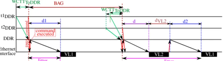
In this paper, we consider that the regulation according to the Bandwidth Allocation Gap (BAG), i.e. the minimum delay between two successive frames, is done at the core which executes the task sending the data to the Ethernet interface, noted tDDR. A task tDDRsends data on a given
t1DDR t2DDR DDR Ethernet Interface WCTTToDDR command executed D MA co mman d VL1 d1 BAG Jitter VL2 VL1 WCTTToDDR Jitter d2 d dVL2
Fig. 4: A possible transmission on a given VL.
VL to an Ethernet interface by following the steps detailed for an outgoing I/O flow in section II. The Ethernet inter-face executes one DMA command at once and so the data are transmitted as NoC packets from the DDR memory to the Ethernet interface. When all the packets are received by the Ethernet interface, the Ethernet frame is created. Then, the Ethernet interface executes another DMA com-mand directly if there is enough place in the buffer or waits to transmit the Ethernet frame on the Ethernet link. This means that we could not simultaneously have two flows transmitted from the DDR to the Ethernet interface. The transmission on a VL to the Ethernet interface can be delayed if a different task is sending on another VL to this Ethernet interface. In an AFDX network, this delay corresponds to the jitter induced by the multiplexing functions of the End System. The goal is now to define this delay in the proposed architecture.
In a NoC architecture, the DMA command from tDDR to the Ethernet interface is sent after the complete trans-mission of the data of the VL from tDDRto the DDR. This transmission delay is obtained by computing the WCTT of the data packets from the core executing tDDR to the DDR. This delay, noted W CT TT oDDR, is thus constant and can be computed as a part of the execution time of the task. This behavior is equivalent to the one in classical End Systems where writing to the memory is a part of the task execution.
Figure 4 shows the different steps of data transmission on a VL, noted V L1, from the task t1DDR. In this example, the task t1DDRsends a VL each BAG period to the AFDX. The interval BAG is counted after W CT TT oDDR. We show in this figure how the data transmission on V L1 can be
impacted by the data transmission on an other VL, noted
V L2from a task t2DDRusing the same Ethernet interface. In the left side of the Figure 4, t1DDRsends the data to the DDR controller. After waiting W CT TT oDDR, t1DDRsends the DMA command to the Ethernet interface. The delay of a DMA command is neglected as it is transmitted on a sep-arate network. When the Ethernet interface executes this DMA command, the data NoC packets are transmitted from the DDR controller to the Ethernet interface. Then, the Ethernet frame is transmitted on the AFDX V L1. The
jitter in this case is equal to d1 which is the transmission
delay for the outgoing I/O flow from the DDR controller to the Ethernet interface. As contentions can appear on the NoC, thus this delay is non constant.
V L2 through the same Ethernet interface, in the same
way as t1. The DMA command sent by t2DDR arrives before the one sent by t1DDR. The commands are stored into a FIFO buffer in the Ethernet interface. Only one DMA command can be executed by the Ethernet interface. The data sent by t1DDR waits in the DDR memory for the complete transmission of the data of t2DDR on the NoC and on the AFDX network. The jitter on V L1 of
the next frame is thus the sum of three delays: (1) the transmission delay of the outgoing I/O flow sent by t2DDR from the DDR to the Ethernet interface, noted by d, (2) the transmission delay of the Ethernet frame on AFDX
V L2from the Ethernet interface to the first AFDX switch,
noted by dV L2, (3) the transmission delay of the outgoing
I/O flow sent by t1DDR from the DDR to the Ethernet interface, noted by d2. Once this transmission is done, the
Ethernet interface commands the transmission of the data of t1 to the Ethernet interface.
In this paper, we consider that each application can send only on a single VL. In a worst case scenario, for an analyzed V Li, the corresponding application appisends the DMA command after all the n avionics applications al-located on the same NoC have sent their DMA command. Therefore, the maximum jitter on a given V Li, i.e. the jitter when considering a worst case scenario, corresponds to: W CT TV Li T oDDR+ n X j=1 j6=i W CT TV Lj T oDDR+ n X j=1 j6=i dV Lj f rame (1) where W CT TV Lj
T oDDRreturns the WCTT of the NoC
pack-ets from the task tDDR, in an application j, to the DDR memory. Besides, dV Lj
f ramecorresponds to the transmission delay of a frame on the Ethernet link for V Lj. As the equation (1) includes the W CT TT oDDRof all applications allocated on the NoC, thus the maximum jitter on all VLs is the same. Let us now see if this jitter does not exceed the maximal allowed jitter, i.e. 500µs.
IV. Problem illustration on a case study In this section, we show on a realistic avionics case study that the existing mapping strategies do not guarantee the maximum jitter of AFDX networks.
A. Motivating case study
The considered case study is composed of critical and non critical applications:
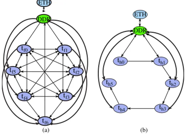
• Full Authority Digital Engine (FADEC) ap-plication: It controls the performance of the air-craft engine. It receives 30 KBytes of data from the engine sensors via an Ethernet interface and sends back 1500 Bytes of data to the engine actuators. The application FADECn is composed of n tasks denoted tf 0 to tf n−1. tf n−1 is dedicated to send the commands to the engine actuators via the Ethernet interface. Except tf n−1, all other tasks exchange 5
Fig. 5: Task graph of core-to-core and core-to-I/O communications of the: (a) FADEC application, (b) HM application.
SHiC M apIO
jitter in µs 676.7 579
TABLE I: Table reporting the jitter for a given VL in function of
SHiC and M apIO strategies when considering the case study A.
KBytes of data. They also send 5 KBytes of data to
tf n−1. Figure 5a shows the tasks graph of F ADEC7.
This graph illustrates the core and core-to-I/O communications between the tasks of the FADEC application.
• Health Monitoring (HM) application: It is used
to recognize incipient failure conditions of engines. It receives through an Ethernet interface, a set of frames of size 130 KBytes and sends back 1500 bytes of data actuators. The application HMn is composed of n tasks, denoted th0 to thn−1. The last task thn−1 is dedicated to send the data actuators to the Ethernet interface. The task thi sends 2240 bytes of data to
thi+1, with i ∈ [0, n − 2]. All these tasks finish their processing by storing their frames into the memory. Figure 5b shows the tasks graph of HM6.
FADEC applications are critical, while HM applica-tions are non-critical. The considered case study, noted A, is composed of 3 FADEC applications: F ADEC13,
F ADEC11, F ADEC7 and five HM applications: HM16,
HM12, HM11, HM10 and HM9. The AFDX network is
connected to the Ethernet interface located at the middle of the NoC. SHiC and MapIO are both used to allocate these applications on a 10×10 Tilera-like NoC.
B. Limitations of existing strategies
Figures 6a and 6b show respectively how SHiC and
M apIO map the applications of the case study A on the NoC. In this paragraph, we focus on the outgoing I/O flows to compute the jitter on a given VL. Table I shows the jitter computed for a given VL using the equation (1). In both cases, the jiiter is greater than the maximum allowed jitter, i.e. 500µs. This jitter depends on the WCTTs of the outgoing I/O flows of the other applications. Figure 7 shows these WCTTs for each mapping strategy.
Let us first consider HM16and F ADEC11. SHiC
port1 port2 port3 port4 port5 4 5 6 7 3 2 1 0 5 6 7 0 1 2 3 4 (10,0) (0,0) 8 9 10 8 9 10 port11 port12 port13 port14 port15 port16 port17 port18 port6 port7 port8 F (0,5) 16 FADEC A C (a) port 1 port 2 port 3 port 4 port 5 4 5 6 7 3 2 1 0 5 6 7 0 1 2 3 4 (10,0) (0,0) 8 9 10 8 9 10 port11 port12 port13 port14 port15 port16 port17 port18 port 6 port 7 port 8 (0,5) 10 FADEC11 H 12 HM (b) port11 port12 port13 port14 port15 port16 port17 port18 10 5 FADEC port1 port2 port3 port4 port5
(10,0) port8 port7 port6 (0,0)
(0,5) 4 5 6 7 3 2 1 0 5 6 7 0 1 2 3 4 8 9 10 8 9 10 (c)
Fig. 6: Mapping for the case study A composed of 8 applications using respectively SHiC, M apIOand ex M apIO.
0 20000 40000 60000 80000 100000 120000 140000 160000 180000 200000
Fadec11 Fadec13 HM11 HM16 HM12 HM10 Fadec7 HM9
W CT T i n ns Applications SHiC MapIO
Fig. 7: A graph illustrating the WCTT of the outgoing IO flows for different applications in function of SHiC and M apIOstrategies
when considering the case study A.
with M apIO. Conversely, the WCTT for F ADEC11 is
higher with SHiC than with MapIO. This difference of values is explained by the way the allocation of these appli-cations is performed. With SHiC, F ADEC11 is allocated
far from the Ethernet interface, while HM16 is allocated
near to this interface. Conversely, MapIOmaps F ADEC11
near to the Ethernet interface, and HM16 far from this
interface. Consequently, the distance of the application to the Ethernet interface varies the number of routers crossed by the outgoing I/O flow to reach the Ethernet interface located at (0,5). Thus, this distance is a factor varying the WCTT of an outgoing I/O flow.
On the other side, HM12 is allocated near to the
Eth-ernet interface in SHiC, while it is allocated far from this interface in MapIO. However, the WCTTs of their outgoing I/O flows are quite the same. Thus, the distance to the Ethernet interface is not the sole factor impacting the WCTT of an outgoing I/O flow. As we can see in Figure 6b, some core-to-core flows of F ADEC13 share
the same path as the outgoing I/O flow of HM16. Then,
the WCTT of the outgoing I/O flow of HM16 depends
on the contentions that experiences this flow on its path, especially on the first line.
Now, let us consider HM9 and F ADEC11 in MapIO.
HM9is allocated further from the Ethernet Interface than
F ADEC11, as shown in Figure 6b. The WCTT of the
outgoing I/O flow of F ADEC11 is much greater than the
HM9one although they share a part of their path. Indeed,
the outgoing I/O flow of HM9is blocked at the source, i.e.
the port 6 of DDR, by six non-blocked flows as illustrated in Figure 6b. On the other side, the outgoing flow of
F ADEC11 is blocked at the source, i.e. the port 2, by
five flows. However, these flows are blocked on their paths by core-to-core flows illustrated in Figure 6b. Then, the source-based contention combined with the contentions on the blocking flows path is another factor varying the WCTT of an outgoing I/O flow.
To overcome the limitations of existing mapping strategies, we propose a mapping strategy, noted ex M apIO, that has the following three objectives: (1) minimize the num-ber of source-based contentions by reducing the numnum-ber of flows coming from the same DDR port used by the outgoing I/O flow, noted pDDR, (2) minimize the path-based contention on the flows coming from pDDR, (3) minimize the path-based contention on the path of the outgoing I/O flow.
V. Proposed mapping strategy: Ex M apIO As M apIO aims to reduce the contentions on the in-coming I/O flows, we propose to extend this strategy. The new strategy adds some rules to M apIO when allocating the tasks within the applications which regions do not intersect with Ethernet interfaces. This section details these rules to reach our objectives.
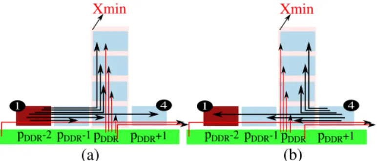
A. Rule 1: Minimizing the number of source-based con-tention
The intermediate port pDDR, used by tDDR to send the outgoing I/O flow to the Ethernet interface, could also be used by other tasks on the same column with
tDDR. The flows sent from pDDR to these tasks generate a contention with the outgoing I/O flow at the source
pDDR. To reduce this contention, the first rule allocates
pDDR pDDR-1 pDDR+1 Xmin (a) pDDR pDDR-1 pDDR+1 Xmin (b) tDDR tDDR 1 3 1 2 3 2 pDDR Xmin (c) tDDR 1 2 3
Fig. 8: A possible scenario when allocating the task with: (a) the maximum IC on the core 1, (b) the maximum EC on the core 3, (c) the maximum IC on 3.
a minimal number of tasks and the nearest one to the Ethernet interfaces. We present in Figure 6c the mapping of the case study A after applying the ex M apIOstrategy. This figure illustrates the columns Xmin selected by this rule for each application.
B. Rule 2: Minimizing the number of flows in contention with the flows coming from pDDR
This rule allocates tDDR and other tasks on Xmin in such a way to generate flows in an opposite direction to the flows coming from pDDR to reduce their contentions. Thus, we build from the tasks graph of each application the lists of tasks sending to tDDRand those receiving from it, noted respectively by LS and LR. Different cases can exist dependent of the size of LS and LR:
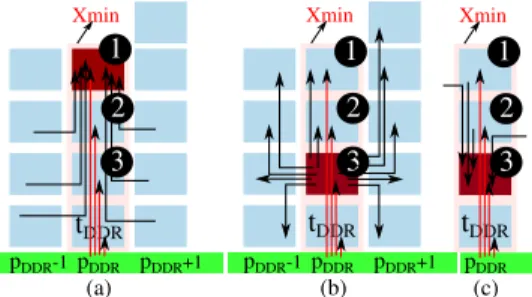
a) Case A: LS = LR = 0: We allocate tDDR on the first line nearest to the DDR memory as there are no tasks that communicate with tDDR. The tasks with the minimum number of ingress communications (IC), i.e. re-ceiving data from a low number of tasks, are then allocated on Xmin. In fact, in Figure 8a, we allocate on the core 1 the task with the maximum number of IC. It is obvious that the flows received by this task, either from its column or other columns, block the flows coming from pDDR. The number of blocking flows is reduced when allocating on the core 3 the task with the maximum number of egress communications (EC), i.e. sending data to a high number of tasks, as illustrated in Figure 8b. As a task with a minimum number of EC could present a high number of IC, we thus allocate the tasks with an increasing number of IC by following the order illustrated in Figure 8c, i.e. from the top to the bottom while approaching to the DDR. Actually, a task with a maximum IC on the core 3, as illustrated in this figure, could receive from other rows above it without blocking the flows coming from DDR. Besides, a selected task should not send to the allocated tasks on Xmin in order to reduce the number of contentions, i.e. the task that will be allocated on 2 should not send to the task allocated on 1.
b) Case B: LS 6= 0 and LR = 0: LS 6= 0 means that tDDRreceives data from the tasks of LS. If we allocate
tDDR at the top, of Xmin as illustrated in Figure 9b, the flows received by this task are in the same direction of the flows going from pDDR and thus they are blocking flows.
(a) (b) pDDR Xmin tDDR pDDR Xmin tDDR (c) (d) pDDR Xmin tDDR pDDR Xmin tDDR 1 2 3 1 2 3
Fig. 9: Different scenarios on Xminwhen allocating: (a) tDDRat the
bottom, (b) tDDRat the top, (c) the task with maximum EC on the
core 3, (d) the task with the maximum EC on the core 1.
Thus, we allocate tDDR at the bottom, near to the DDR, as illustrated in Figure 9a. As the tasks in LS send data to
tDDR, thus we have to begin their allocation on Xminfrom the bottom to top with the increasing minimum number of EC. In fact, allocating a task with the maximum EC on the core 1, as in Figure 9d, generates flows in contention with the flow coming from the DDR, which is not the case when this task is allocated on the core 3, as shown in Figure 9c. Besides, each selected task should not receive data from the tasks allocated on Xmin, i.e. the task that will be mapped on the core 2 should not receive data from the task allocated on 1. Finally, when it remains a number of unallocated cores on Xmin, the case A is thus applied. For example, for HM12, LSincludes only th10that sends data to tDDR, i.e. th11. th11 is first allocated at the core at (8,2), while th10 is allocated above it. The case A now applies to allocate th0, task with minimum IC, at (8,5), while th1 is allocated at (8,4).
c) Case C: LS = 0 and LR 6= 0: This case is the opposite scenario of the case B. Here, tDDR sends data to the tasks in LR, and thus this task should be now allocated at the top of Xmin, far from the DDR. In this way, the flows received by these tasks are in the opposite direction with the flows coming from pDDR. Unlike the case B, here the allocation begin from the top to bottom by ordering the tasks in LRwith an in increasing number of IC. Besides, each selected task should not send data to the allocated tasks to avoid a contention with any flow coming from pDDR.
d) Case D: LS 6= 0 and LR 6= 0: This case associates the cases B and C: tDDRsends data to the tasks of LR and receives from the tasks in LS. Thus, tDDR is now allocated somewhere on Xmin in such a way the case B is applied above tDDRand the case C below it. Figure 10 shows that we must begin by allocating the tasks of LS. In Figure 10a, we allocate all the LS tasks above tDDR and some tasks of LR below it, while in Figure 10b, all the
LR tasks are allocated below tDDR. In the first case, the remaining tasks of LR, not allocated on Xmin, receive the flows from tDDR without causing any contention with the flows coming from pDDR. However, in the second case, the flows generated by the remaining tasks of LS are blocking flows. Thus, when the tasks of LS could not fill all Xmin, then tDDR is allocated on the core corresponding to the
pDDR pDDR-1 pDDR+1 Xmin (a) (b)
t
DDR pDDR pDDR-1 pDDR+1 Xmin 1t
DDR 1 2 1 2 3 4 5 3 4 5 All LS From LR From LS All LRFig. 10: A possible scenario when allocating all the tasks of: (a) LS,
(b) LR, on Xmin
difference between the size of LS and the size of Xmin. However, when the size of LS is greater than the size of (Xmin− 1), we allocate tDDR at the second line near the DDR. In this case, we allocate a high number of tasks from
LS on Xmin and only one task from LR.
In all the cases, the remaining tasks from LS are thus allocated on the same line of tDDR and on its right, while those of LR are allocated on the same line with tDDR but on its left if possible.
C. Rule 3: Minimizing the path-based contention on the first line used by the outgoing I/O flows
This rule is only applied on the applications presenting an intersection with the DDR. The remaining tasks are ordered in two lists, noted LGS and LGR. These tasks are ordered with an increasing number of EC in LGS, while in LGR with the increasing number of IC. Therefore, we begin by the lowest degree of communications from
LGS and then from LGR. A task with degree 0 in LGS means that the task does not send data to any other tasks. The placement of the task on the first line depends from which list is selected. Indeed, a task selected from
LGS is allocated on the most left core of the first line. Actually, allocating a task with the maximum number of EC on the most left core, as at the core 1 of Figure 11a, generates blocking flows not only to the outgoing I/O flow on the first line but also to those coming from pDDR. These blocking flows are reduced when allocating this task at the core 4 as seen in Figure 11b. Besides, the selected task should not receive from the allocated tasks on its left on the same line, and not send the allocated tasks on its right. By following the same principle, a task selected from LGR is thus allocated on the most right of the first line.
For HM11, LGS= (degree1 : th9, th8...th0) and LGR = (degree0 : th0; degree1 : th8...th1). The lowest degree, i.e. degree 0, is only in LGR where the task selected is th0. It is allocated on the most right of the first line, i.e. at (5, 1). The other tasks present the same characteristics, thus they are allocated arbitrary on this first line.
D. Rule 4: Minimizing the contentions on the flows coming from the DDR
In order to allocate the remaining tasks on the remain-ing cores, we begin the allocation from the second line,
pDDR pDDR-1 pDDR+1 Xmin
(a)
(b)
pDDR-2 1 4 pDDR pDDR-1 pDDR+1 Xmin pDDR-2 1 4Fig. 11: A possible scenario when allocating the task with the maximum EC on: (a) the core 1, (b) the core 4.
near the DDR (it is the first line for the applications that
do not have any intersection with the DDR), to the lines
at the top of the application. The tasks with the minimum number of EC are allocated first. Actually, a task with the maximum number of EC allocated at the last line generate flows in opposite direction with the flows coming from the DDR. Besides, it is preferable to select the tasks that send data to the tasks already allocated on the same line, and also that do not receive from the allocated tasks below its line and do not send to the allocated tasks above its line.
E. Rule 5: Modifying pDDR for an outgoing I/O flow for
an application
At this level, all tasks are allocated within their appli-cations. However, there are some applications presenting an all-to-all communications (like FADEC). Thus, it is impossible to reduce significantly the contentions with the outgoing I/O flow when they are allocated on the first line. For this reason, this rule aims to change pDDR for/from which the outgoing I/O flow is sent when the contention on the first line is not reduced. However, this change is subject to some conditions. In fact, we first compute the charge of the contentions on the outgoing I/O flow on the column of pDDR, noted chargey, and on the first line from
pDDR, noted chargex. Then, we do another computation of these charges when changing pDDRto pmDDR. pmDDR is the first DDR port not used by another outgoing I/O flow (except the ports 1 and 11 to not add a contention on the incoming I/O flow). Only when the total charge is reduced, we confirm the change of the DDR port. chargex and chargey are calculated as following:
chargex= NF L f lows NF L routers ; chargey= Nf lowsCpDDR NroutersCpDDR (2) NF L
f lows returns the number of flows having the same
direction as the outgoing I/O flow on the first line. These flows are considered on the routers counted by NF L
routers which are computed from the next port of the peripheries of the concerned application. On the other side, NCpDDR
f lows corresponds to the number of flows going on the same direction of the flows coming from pDDR on its column.
NCpDDR
routers returns the number of cores on which the tasks allocated to them use pDDR.
SHiC M apIO ex M apIO
jitter in µs 676.7 579 436.5
TABLE II: Table reporting the jitter for a given VL in function of mapping strategies when considering the case study A.
Before applying this rule on HM16, its outgoing I/O
flow, going from the port 17, is blocked by a number of flows from the 36 flows of FADEC going in the same direction with it, as illustrated in Figure 6c. The number of routers are counted from the port 16 which comes after the peripheries of HM16, thus Nrouters = 7. Therefore,
chargex = 367 = 5.14. However, chargey = 0 as there are no core-to-core flows on HM16going on the same direction
with the flows coming from pDDR. Let us now recompute the charge for HM16if the port used by its outgoing I/O
flow is 13. Thus, the number of flows going on the same direction on the routers counted from the port 13, i.e. on 4 routers, is reduced to 9. Then, chargex = 94 = 2.25. However, chargey is increased. Indeed, the port 13 is used by F ADEC13and HM10, thus there are 4 routers use the
port 13. On these routers, there are 7 flows going in the same direction with the flows coming from the DDR, as illustrated in Figure 6c. Thus, chargey =74 = 1.75. As the total charge is reduced to 4, then the outgoing I/O flow for HM16 goes from the port 13.
VI. Evaluation
This section evaluates ex M apIO compared to the
SHiC and M apIO strategies. Thus, we first compare the jitter obtained with the existing mapping strategies on the case study A illustrated in section IV. We then explain the impact of the different rules on the WCTTs of the outgoing I/O flows. Then, we consider another realistic case study in order to show the impact of the number of applications allocated on the NoC on the jitter of an outgoing I/O flow.
A. Evaluation of the jitter on different sizes of NoCs 1) 10×10 NoC: Figures 6a, 6b and 6c illustrated the
mapping of the case study A by considering the different mapping strategies. Table II reports the jitter value for a given VL in function of these strategies. This table shows that only by applying ex M apIO, the jitter is reduced by respectively 35% and 11.5% compared to SHiC and
M apIO. This reduction is sufficient to lead to a jitter lower than 500µs.
To explain this reduction, we consider the graph in Figure 12 which shows the WCTTs of the outgoing I/O flows for the different applications in function of the mapping strategy. The WCTT of the outgoing I/O flow of F ADEC11 is reduced by 33% compared to M apIO. Indeed, this reduction is due to the rule 2, where tf 10, i.e.
tDDR is placed at the bottom of the application reducing the contention on the column of the port 2. In M apIO, this task receiving from all other tasks is placed at the top of the column.
The rule 1 has especially reduced the WCTT of HM12and
HM11by 28% compared to M apIO. Actually, in M apIOin 0 20000 40000 60000 80000 100000 120000 140000 160000 180000 200000 W C T T i n n s Applications
Fadec11 Fadec13 HM11 HM16 HM12 HM10 Fadec7 HM9
SHiC MapIO ex_MapIO
Fig. 12: A graph illustrating the WCTT of the outgoing IO flows for different applications in function of mapping strategies when considering the case study A.
SHiC M apIO ex M apIO
jitter in µs 446.5 406 354.6
TABLE III: Table reporting the jitter for a given VL in function of mapping strategies when considering the case study B.
Figure 6b, th11 in HM12, i.e. tDDRis allocated on the last column, thus the outgoing I/O flow going from the port 8 is blocked at the source by 8 flows going from this port to the last two columns. However, the rule 1 allocates th11 on Xmin, then the outgoing I/O flow goes from the port 7 and it is blocked at the source by 4 flows. Besides, the rule 3 eliminates some flows that was in the same direction with the outgoing I/O flows, as the flow from th2 to th3in
HM11 in M apIO.
Finally, the WCTT of the outgoing I/O flow of HM16
is reduced by 55.2% compared to M apIO, but it is still greater than the one obtained by SHiC. In fact, in the
SHiC mapping illustrated in Figure 6a, HM16 is the
nearest Ethernet interface. This is not the case in M apIO and ex M apIO, where this flow is blocked by core-to-core flows of FADEC. The rules 1 and 2 reduce the WCTT of this flow by 11, 11% compared to M apIO. These rules allocate th15at the 8thcolumn, and thus the outgoing I/O flow from HM16 is blocked at the source by 5 unblocked
flows, while it was blocked by 11 flows in M apIO, as t15
is on the last column. On the other hand, the rule 5 has the greatest impact on decreasing the WCTT of this flow by 44.09%. Indeed, the rule 5 has reduced the distance crossed by the outgoing I/O flow, from 14 to 9 routers, and thus it decreases the number of flows in congestion with it.
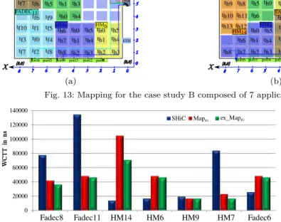
2) 8×9 NoC: We consider a case study, noted B,
consisting of 7 applications allocated on a NoC of size of 8 × 9. This case study is made of F ADEC11, F ADEC8,
F ADEC6, HM14, HM9, HM7and HM6. Figures 13a, 13c
and 13b show respectively the mapping of these applica-tions by considering SHiC, M apIO and ex M apIO.
Table III shows that the jitter in all strategies is less than 500µs. The jitter in ex M apIO is reduced by respectively 20.5% and 12.9% compared to other strategies. Besides, the jitter obtained in SHiC is close to the maximum allowed jitter. ex M apIO can reduce the WCTTs of the
port1 port2 port3 port4 port5 4 5 6 7 3 2 1 0 5 6 7 0 1 2 3 4 (8,0) (0,0) 8 8 9 port11 port12 port 3 port14 port15 port16 port6 (0,5) A C FADEC (a) port1 port2 port3 port4 port5 4 5 6 7 3 2 1 0 5 6 7 0 1 2 3 4 (8,0) (0,0) 8 8 9 port11 port12 port13 port14 port15 port16 port6 (0,5) 14 1 FADEC (b) port1 port2 port3 port4 port5 4 5 6 7 3 2 1 0 5 6 7 0 1 2 3 4 (8,0) (0,0) 8 8 9 port11 port12 port13 port14 port15 port16 port6 (0,5) 11 9 FADEC (c) Fig. 13: Mapping for the case study B composed of 7 applications using respectively SHiC, M apIOand ex M apIO.
0 20000 40000 60000 80000 100000 120000 140000
Fadec8 Fadec11 HM14 HM6 HM9 HM7 Fadec6
SHiC MapIO ex_MapIO
W C T T i n n s Applications
Fig. 14: A graph illustrating the WCTT of the outgoing IO flows for different applications in function of mapping strategies when considering the case study B.
outgoing flows for HM7, HM9, F ADEC11and F ADEC8,
as shown in the graph of Figure 14. However, by comparing to SHiC, the WCTTs of HM6, HM14 and F ADEC6
are still higher. Indeed, SHiC allocates HM6 and HM14
near to the Ethernet interfaces, thus the congestion is reduced. Although F ADEC6 is allocated near to the
Ethernet interfaces in ex M apIO, the increased value of its outgoing flow is explained by the contentions with the flows of F ADEC11. Actually, this flow goes from the port
12 and crosses more than 3 routers occupied by FADEC. However, in SHiC the outgoing flow is not blocked by a high number of flows at the first line as it crosses only one router occupied by F ADEC. Therefore, if we increase the size of F ADEC6, the WCTT of its outgoing flow in
SHiC will increase, as the congestion at the source and
possibly on the first line increases, which lead to a high jitter. However, the WCTT of the outgoing I/O flow of
F ADEC6in ex M apIOstill the same as its value depends on the mapping of F ADEC11 which is not modified.
B. Impact of the number of applications on the jitter
As the jitter depends on the WCTTs of the outgoing I/O flows of the different applications, thus theoretically adding a new application increases the jitter. In order to show the impact of adding applications on the jitter in the different mapping strategies, we consider an extension of the case study A where we add the application HM7.
As ShiC strategy is unable to allocate this application,
port1 port2 port3 port4 port5 4 5 6 7 3 2 1 0 5 6 7 0 1 2 3 4 (10,0) (0,0) 8 9 10 8 9 10 port11 port12 port13 port14 port15 port16 port17 port18 port6 port7 port8 (0,5) FADEC 13 1
Fig. 15: M apIO mapping for the case study A when adding a new
application HM7. port1 port2 port3 port4 port5 4 5 6 7 3 2 1 0 5 6 7 0 1 2 3 4 (10,0) (0,0) 8 9 10 8 9 10 port11 port12 port13 port14 port15 port16 port17 port18 port6 port7 port8 10 (0,5) HM 13 FADEC
Fig. 16: ex M apIO mapping for the case study A when adding a
new application HM7.
the mapping of this case study is the same in Figure 6a.
M apIO and ex mapIO allocate the 9 applications as illustrated respectively in Figures 15 and 16.
As SHiC leaves the same mapping, the jitter remains unchanged as shown in Table IV. However, this jitter is increased by 28% in M apIO and ex mapIO compared to the case study A made of 8 applications. Actually, adding an application leads not only to add the WCTT of its outgoing I/O flow but also increases the congestion on
SHiC M apIO ex M apIO
jitter in µs 676.7 744.3 558.2
TABLE IV: Table reporting the jitter for a given VL in function of mapping strategies after adding a new application to the case study A.
SHiC M apIO ex M apIO
jitter in µs 514 483.7 352.13
TABLE V: Table reporting the jitter for a given VL in function of mapping strategies after adding a new application to the case study B.
the other applications. When increasing the number of the applications, F ADEC11 occupies more routers in the first
line. Then the WCTTs of the outgoing I/O flows of HM11,
HM10and HM8 increase having these flows blocked by a
high number of core-to-core flows of F ADEC11, as shown
in Figures 15 and 16. On the other hand, F ADEC11
occupies a less number of rows and thus the contention on the flows coming from the port 2, i.e. used by the outgoing I/O flow for F ADEC11, is reduced.
Now, we consider the case study B, and we add a new application HM5. We also decrease the size of F ADEC8
to 7, HM14 to 10 and HM9 to 8, in order to make SHiC
allocates all the applications. Here, the jitter increases with SHiC and M apIO and exceeds the maximum al-lowed jitter with SHiC. However, it remains the same with ex M apIO. Indeed, decreasing the size of some applications will decrease the WCTTs of their outgoing I/O flows. However, adding an application increases the congestion on the other applications. These congestions are reduced by applying our rules, but this is not the case when allocating the applications using M apIO and SHiC strategies.
C. Discussion
The results presented in the previous section show that the jitter is a function of the type, the size of the applications and the size of the NoC. Considering different NoC sizes, we have seen that ex M apIO reduces the WCTTs of the outgoing I/O flows and thus the jitter on a given VL. This jitter is lower than 500µs when allocating 8 applications. However, when increasing the number of applications (without modifying the size of the other ap-plications) on a 10×10 NoC, the jitter exceeds 500µs. This is explained by adding a WCTT on the jitter as Equation 1 indicates. Besides, this new application adds a congestion on the outgoing I/O flows from other applications. On a reduced size of a Tilera-like NoC, we have seen that till 8 applications, ex M apIOleads to a jitter lower than 500µs. Therefore, our proposition explained in section III presents some limitations where ex M apIOis applied with specific NoCs and applications sizes.
VII. Conclusion and future work
In this paper, we proposed to replace the mono-core processors in the avionics architecture by a NoC-based many-core architecture. Thus, in the proposed architecture the End Systems are based on NoC.
The main contributions in this paper are:
• First, the description of the integration problem of the NoC in an AFDX architecture in order to keep the same functions and characteristics of the current End Systems.
• Second, the illustration on an avionics case study, where we show the limitations of existing mapping strategies to reduce the jitter for a given Virtual Link.
• Third, the description of a new mapping strategy which adds a number of rules to an existing strategy,
M apIO, in order to reduce the jitter. These rules min-imize the source-based and path-based contentions on the path of the outgoing I/O flows.
• Finally, our new mapping strategy evaluation,
per-formed on realistic avionics case studies, which shows that the jitter is significantly reduced (up to 34%). Meanwhile, the jitter increases with the increase of the NoC and the applications size, leading to exceed the maximum allowed bound.
As future work, we aim to evaluate our proposed map-ping strategy on different NoCs and applications sizes to find the threshold of these parameters that guarantee a bounded jitter. Besides, another proposition making the NoC behaves as a current End System is expected, as considering one dedicated core to shape the traffic and schedule the outgoing I/O flows in such a way to bound the jitter.
References
[1] L. Abdallah, M. Jan, J. Ermont, and C. Fraboul. Wormhole networks properties and their use for optimizing worst case delay analysis of many-cores. In 10th IEEE International Symposium
on Industrial Embedded Systems (SIES), pages 59–68, Siegen,
Germany, June 2015.
[2] L. Abdallah, M. Jan, J. Ermont, and C. Fraboul. Reducing the contention experienced by real-time core-to-i/o flows over a tilera-like network on chip. In Real-Time Systems (ECRTS),
2016 28th Euromicro Conference on, pages 86–96. IEEE, 2016.
[3] C. de Souza, L. Ewerson, N. Calazans, V. Laert, and F. Moraes. Dynamic task mapping for mpsocs. Design & Test of Computers, 27(5):26–35, 2010.
[4] M. Fattah, M. Daneshtalab, P. Liljeberg, and J. Plosila. Smart hill climbing for agile dynamic mapping in many-core systems. In
Proc. of the 50th Annual Design Automation Conference, page 39,
2013.
[5] M. Fattah, M. Ramirez, M. Daneshtalab, P. Liljeberg, and J. Plosila. Cona: Dynamic application mapping for congestion reduction in many-core systems. In 30th Intl. Conf. on Computer
Design (ICCD), pages 364–370, 2012.
[6] T. Ferrandiz, F. Frances, and C. Fraboul. A method of com-putation for worst-case delay analysis on SpaceWire networks. In Proc. of the 4th Intl. Symp. on Industrial Embedded Systems
(SIES), pages 19–27, Lausanne, Switzerland, July 2009.
[7] T. Ferrandiz, F. Frances, and C. Fraboul. Using Network Calculus to compute end-to-end delays in SpaceWire networks.
SIGBED Review, 8(3):44–47, 2011.
[8] D. Wentzlaff, P. Griffin, H. Hoffmann, and al. On-chip intercon-nection architecture of the tile processor. IEEE Micro, 27(5):15– 31, 2007.
[9] C. Zimmer and F. Mueller. Low contention mapping of real-time tasks onto tilepro 64 core processors. In 18th Real-Time
and Embedded Technology and Applications Symposium (RTAS),