HAL Id: hal-03156540
https://hal.archives-ouvertes.fr/hal-03156540
Submitted on 2 Mar 2021HAL is a multi-disciplinary open access
archive for the deposit and dissemination of sci-entific research documents, whether they are pub-lished or not. The documents may come from teaching and research institutions in France or abroad, or from public or private research centers.
L’archive ouverte pluridisciplinaire HAL, est destinée au dépôt et à la diffusion de documents scientifiques de niveau recherche, publiés ou non, émanant des établissements d’enseignement et de recherche français ou étrangers, des laboratoires publics ou privés.
Determining the validity domain of roughness
measurements as a function of CD-SEM acquisition
conditions
Mohamed Abaidi, Jordan Belissard, Nivea Schuch, Thiago Figueiro, Matthieu
Millequant, Jonathan Pradelles, Loïc Perraud, Aurélien Fay, Jessy Bustos,
Jean-Baptiste Henry, et al.
To cite this version:
Mohamed Abaidi, Jordan Belissard, Nivea Schuch, Thiago Figueiro, Matthieu Millequant, et al.. Determining the validity domain of roughness measurements as a function of CD-SEM acquisition conditions. SPIE Advanced Lithography, Feb 2021, Online Only, France. pp.36, �10.1117/12.2584040�. �hal-03156540�
1
Determining the validity domain of roughness measurements as a
function of CD-SEM acquisition conditions
Mohamed Abaidi¹, Jordan Belissard¹, Nivea Schuch¹, Thiago Figueiro¹, Matthieu Millequant¹, Jonathan Pradelles², Loïc Perraud², Aurélien Fay², Jessy Bustos², Jean-Baptiste Henry², Estelle Guyez², Sébastien Berard-Bergery², Patrick
Schiavone¹ ³
1 Aselta Nanographics, 4, place Robert Schuman, 38000 Grenoble, France 2 Univ. Grenoble Alpes, CEA, Leti, F-38000 Grenoble, France
3 Univ. Grenoble Alpes, CNRS, CEA/LETI-Minatec, Grenoble INP, LTM, F-38054 Grenoble-France
ABSTRACT
In the effort of continuously improving patterning strategies for increasing circuit density while reducing dimensions, several challenges regarding patterning fidelity emerge. In recent years, stochastic effects had their relative importance increased, and therefore the need for closely monitoring those effects is also increasing [1]. Among other stochastic effects, within-feature roughness is significant as it can impact circuit electrical behavior, decreasing time and power performance, and even lead to failures. The workhorse method of the industry for measuring roughness is based on top-down CD-SEM (Critical Dimension Scanning Electron Microscopy) image. In recent years, methods have been proposed as a way to improve and standardize the roughness measurement [2, 3]. Those methods rely on the obtention of the power spectral density (PSD) from the detected edges of the features in CD-SEM images, in order to determine their roughness. However, one important aspect is the impact of the CD-SEM image acquisition conditions on the limitation of the observed PSD. As the acquisition parameters changes, different frequencies may be more or less observable in a CD-SEM image, potentially leading to errors in the metrology evaluation [4].
The goal of this study is to first, present the impact of the CD-SEM image acquisition conditions in the roughness measurement, and, second, propose a method to determine the validity domain of the roughness measurements as a function of the acquisition conditions. The proposed method relies on a compact SEM model. This model is calibrated based on experimental CD-SEM images, from several acquisition conditions and design samples. Using this model, synthetic CD-SEM images are generated with a known sample, including its programmed roughness signature (input-PSD), defined by a constant PSD (white noise). The next step relies on a robust-to-noise edge detection algorithm [5], which is then used to compute the PSD by applying the method proposed in [4]. As the input-PSD is known, it is possible to compute the transfer function of the acquisition system [6], for each of the evaluated acquisition conditions. We call ‘limit-PSD’ the transfer function which may be considered as the signature of the acquisition conditions in the frequency domain, and it defines the validity domain of the roughness measurements.
Keywords: Roughness, contour metrology, PSD validity domain, image acquisition conditions, SEM model, synthetic
SEM images
1. INTRODUCTION
Stochastic effects are growing in importance as the feature dimensions are being reduced. Monitoring those effects is part of the challenges for continuously enabling the advances in semiconductor resolution limits and benefit from the scaling effects [1]. One of the significant stochastic effects is within-feature roughness. Measuring unbiased line width roughness (LWR) based on CD-SEM top view images has become standard and is addressed in several papers in the past years [2, 3, 4].
Generally, and in this paper, "line roughness" corresponds to the roughness over the length of the line. There are several ways to characterize the line roughness quantitatively. Whatever method is used, it is notable that roughness has, nominally, decreased with the advancement of technological nodes, while the line roughness over the CD ratio has increased significantly in recent years, which puts more pressure on finding an accurate way of measuring it.
Line roughness is linked to the physic-chemical phenomena driven by materials or the manufacturing process; it has a negative impact on energy consumption as well as on component performance. It is therefore important to measure this parameter in order to be able, if not to reduce it, at least monitor it.
2
In this work a methodology to determine the impact of the CD-SEM image acquisition conditions over the observed roughness measurement is proposed. This is illustrated by a validity domain, or the region where a PSD may be relied upon as an indicator of the actual roughness of the sample. We call ‘limit-PSD’ the transfer function which may be considered as the signature of the acquisition conditions in the frequency domain, and it defines the validity domain of the roughness measurements. For presenting this limit-PSD, both experimental CD-SEM images and synthetic images are used. The first set is used to calibrate the synthetic SEM model while the second is used to have an exact roughness reference.
2. FRAMEWORK FOR ROUGHNESS AND MEASUREMENT SYSTEM ANALYSIS
2.1 Roughness analysis:
During advances in roughness measurement in general, it was shown that expressing roughness as a simple standard deviation of the edge position was not sufficient. As Figure 1 suggests, it is possible to measure the same standard deviation value for two signals with completely different behaviours. Not only those two edge roughness signatures are different, their influence in the circuit behavior is different as well.
Figure 1: Representation of two line edges for an identical standard deviation value σ = 2 nm but a different frequency behavior.
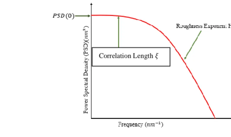
2.1.1 Power spectral density (PSD)
The Power Spectral Density (PSD) of a random process is the Fourier transform of the autocorrelation function.
It is well recognized [7] that the PSD of a resist roughness has an auto-affine behavior that can be expressed by the form given in Figure 2.
3
Equation 1 𝑃𝑆𝐷(𝑓) = 𝑃𝑆𝐷(0)
1+|2𝜋𝜉 𝑓|2𝐻+1
Figure 2 : Power Spectral Density of an auto-affine random process as typically found for resist roughness measurement
2.1.2 Power Spectrum (PS)
Another frequency domain representation of a random signal that will be used along this paper is the Power Spectrum. 𝑃𝑆(𝑓) =1
𝑇 ∫ 𝐹𝑥𝑥(𝑡)𝑒
−2𝑖𝜋𝑚𝑓1𝑡𝑑𝑡 𝑚 = 0,1,2,3, … … … …
𝑇
0 Equation 2
Where 𝐹𝑥𝑥 are autocorrelation functions
2.2 Linear systems characterization
2.2.1 Modulation transfer function (MTF)
The response of a linear system or instrument can be characterized by its modulation transfer function (MTF), determining the bandwidth of the instrument. In the framework of roughness measurement, the MTF contains contributions from the instrumental electron system (including detector and signal processing) as well as the software algorithm used to extract edge position. Generally, these contributions are difficult to account for separately. In this paper, we make use of a “synthetic” approach that allows splitting the contribution of the different contributors from the roughness measurement flow. The MTF is typically evaluated by comparing the PS or (PSD) distribution measured at the output of the system when using a known input. It is typically defined as the square root of the ratio of the measured and simulated PS (PSD) distributions gives the MTF of the instrument [6].
𝑀𝑇𝐹𝑃𝑆= √ 𝑃𝑆𝑜𝑢𝑡𝑝𝑢𝑡
𝑃𝑆𝑖𝑛𝑝𝑢𝑖𝑡 Or 𝑀𝑇𝐹𝑃𝑆𝐷= √
𝑃𝑆𝐷𝑜𝑢𝑡𝑝𝑢𝑡
𝑃𝑆𝐷𝑖𝑛𝑝𝑢𝑡 Equation 3
In the rest of this paper, otherwise specified, we use the MTF computed from the Power Spectrum.
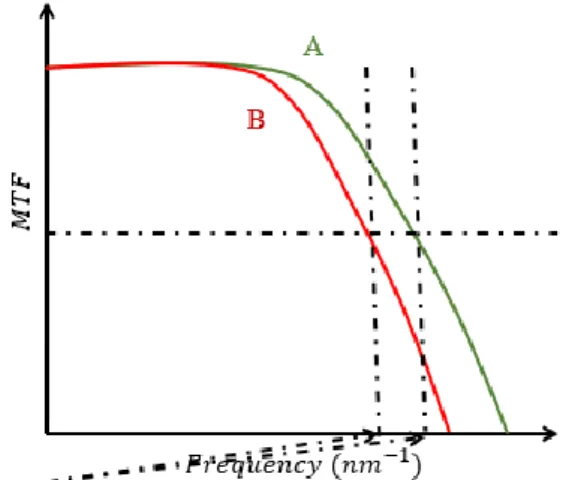
2.2.2 Cutoff frequency
If we see the roughness measurement flow as a low-pass system, we can define a cut-off frequency above which the response of the system (here the roughness measurement) is considered as degraded. The cut-off frequency can be specified in the spatial-frequency domain as the frequency at which the MTF falls below a particular threshold (which is typically chosen at 0.5 when the MTF is defined from the Power Spectrum ratio).
Cut-off frequency provides a single-number to characterize the system and as such it is often seen as being more convenient to use than MTF (which is a function instead of a single number). However, MTF provides a more complete information since it includes information about system performance over a range of spatial frequencies. As we can see in Figure 3 (a), two systems may have identical limiting resolution but different performance at lower frequencies the system corresponding to the higher of the two curves would probably be considered of better information-preserving quality.
4
Figure 3 : Cutoff specifies only the limiting frequency, not the performance at other frequencies.
3. METHODOLOGY
The MTF approach has been used experimentally by Babin et al. [6] who designed a sophisticated input test sample with continuously varying spatial frequencies to characterize metrological equipment. In this paper, we use the same classical concept coupled with several software bricks. In the framework of a roughness measurement flow (that can be seen as a complete linear system) our goal is to better illustrate the interest of the approach and also to be able to identify separately the different contributors to the roughness measurement chain and the potential limitations.
For a random signals process, such as roughness, the ideal test for measuring the transfer function is to have white noise as an input. It is experimentally not possible for us to have experimental images with white noise rough patterns. So our flow is instead to generate synthetic rough pattern with edges presenting a white noise type of roughness. Then, using a compact model well calibrated on experimental images, we generate synthetic SEM images of these rough patterns, extract the edge position and evaluate the PSD or PS of the rough edges
After we have measure the power spectrum of this images and we deduce the MTF at different steps of the flow from Equation 1. This is illustrated in Figure 4.
5
(a)
(b)
(d) (c)
Figure 4 : The different steps of the synthetic flow (a) Input Power Spectrum measured from the white noise rough layout (b) Synthetic image generated using the white noise rough layout as an input (c) Power spectrum of the edge roughness measured from the synthetic image (d) MTF defined from Equation 3 and cutoff frequency defined in the
spatial frequency domain
3.1.1 Synthetic Image Generation of rough patterns
The proposed method relies on the quality of the synthetic images used. We need images that are close to reality
For that, we have three major steps: The first is SEM model calibration from experimental image; the second is noise model calibration from experimental image. The last step last step consists in the calculation of the PSD, also from
6
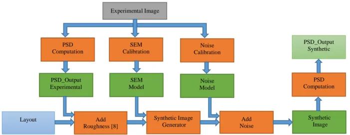
experimental image; this is needed in order to obtain PSD (0) to set the white noise level; the flow is summarized on in Figure 5:
Figure 5: The flow which represents the models necessary to generate the synthetic images
3.1.2 Experimental SEM model calibration
The purpose of this study is to study the SEM profile for experimental images with different landing energy 500eV, 800eV and 3500eV. The main characteristics of the SEM signal are the peak, the median and the bottom (Figure 6);
Figure 6 : SEM profile
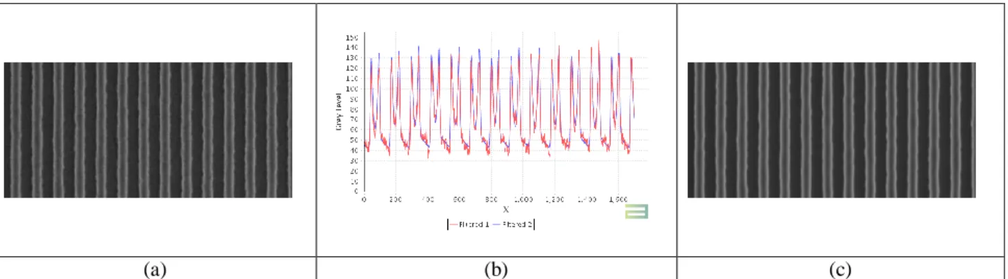
We used the internal software of Aselta Nanographics to calibrate the parameters of the SEM profile. The model is the used to generate a synthetic image from the input rough contour (Figure 7). This SEM model, calibrated to as close as possible from the experimental images allows simulating the SEM profile. On the other hand, we also need to calibrate the noise. This is achieved in it is the next section (3.1.3)
(a) (b) (c)
Figure 7 : (a) Experimental SEM image; (b) Cross-section plot of experimental (red) and synthetic (blue) SEM image; (c) synthetic SEM image
PSD_Output Experimental SEM Model Noise Model PSD Computation SEM Calibration Noise Calibration Experimental Image
7
3.1.3 Experimental SEM Noise model calibration
The intensity noise model is based on the assumption that experimental SEM images contain both additional and multiplicative noise defined by normal distributions.
Inoisy= Iref× 𝒩(1, σm) + 𝒩(0, σa)
σm and σa are respectively the normal distribution standard deviation of the multiplicative and the additional noises.
IrefIs the reference image (simulated by the SEM model, without any noise) and Inoisy is the noisy synthetic image.
Based on this expression, the variance of the signal intensity is defined by the following formula: var(Inoisy) = Iref2 σm2 + σa2
To calibrate the intensity noise model we use an experimental image with a line-space pattern. This type of pattern allows us to extract the mean profile along image lines which is a good estimator of the reference intensity. The variance of the intensity on each column of the image is then reported on the scatter plot and the previous formula of the image variance is fitted on these data (see the figure below).
Figure 8: Intensity noise model calibration from experimental SEM image (left) and a quadratic fit (right) to estimate the multiplicative and additive noise standard deviations.
3.1.4 PSD computation
The last part is the calculation of the PSD from an experimental image (blue framed image Figure 9), we used the Welch method to extract the PSD [7], see Figure 9 blue curve. After extracting the PSD from an image, we can fit the equation (Equation 3), and also fit the noise plateau from the experimental PSD to get the black curve in Figure 9 as well as the roughness PSD parameters (𝑃𝑆𝐷0= 100, 𝜉 = 28 , 𝐻 = 0.5 𝑎𝑛𝑑 𝑁𝑜𝑖𝑠𝑒 = 1).
8
Figure 9 : PSD computed from experimental image edges after contour extraction
3.1.5 Validation of the Synthetic Image Generator
To validate the different steps of our flow (Figure 10), we created synthetic images from an experimental image and compared the outputs (SEM profile, PSD, roughness parameters …)
Figure 10 : Flow for the generation of synthetic images of rough patterns
After generating the synthetic image, (orange framed image Figure 11 (a)), we extracted the PSD from the synthetic image orange curve (Figure 11 (a)). After, we can compare the PSD (biased and unbiased) from the experimental image and synthetic image. Notice that both are very similar (Figure 11 (a)). If we remove the noise (unbiased PSD) the result is even closer (Figure 11 (b)). If we extract the Line Edge Roughness from the PSDs after Equation 4, we can see that again, the results are very close (0.04 nm (see table from Figure 11(b)), almost within the uncertainty of the measurement.
This gives a good confidence about the validity of our approach and about the inferences we can make from it 𝐿𝐸𝑅 = √∫ 𝑃𝑆𝐷(𝑓)𝑑𝑓 (𝐿𝐸𝑅 ≈ 1𝜎) Equation 4 Layout Add Roughness [8] Synthetic Image Generator Add Noise Synthetic Image PSD_Output Experimental SEM Model Noise Model PSD Computation SEM Calibration Noise Calibration Experimental Image PSD Computation PSD_Output Synthetic
9
PSD (a) Unbiased PSD (b)
Experimental Image Synthetic Image LER 1.16 nm 1.13 nm
Experimental Image Synthetic Image LER 0.85 nm 0.81 nm
Figure 11 : Comparison between experimental image and synthetic image. (PSD, unbiased PSD and the respective LER), and visual comparison between experimental and synthetic images (a)
4. THE APPLICATION OF THE TRANSFER FUNCTION APPROACH TO ROUGHNESS
MEASUREMENT
4.1 Define the domain of validity of a rough sample measurement
For a given roughness extraction flow, characterized by a MTF, one can assess whether a particular sample, with a roughness characterized by its “theoretical” PSD can be measured without information loss. Indeed, each input-PSD (simulated or experimental) being ‘below’ the gauge curve defined by 𝑀𝑇𝐹 ∗ 𝑃𝑆𝐷0, the sample to be measured is within
the validity domain of the measurement system (as a whole). However, if the measurement cannot fit below the gauge, some roughness information is expected to be lost. Such relationship is illustrated in Figure 12, presenting one case where the input-PSD is inside the validity domain and another where the actual roughness measurement is expected to be corrupted by a filtering of its high spatial frequency content.
10
Figure 12 : This figure illustrates different PSDs, for the same set of acquisition conditions. The 𝑀𝑇𝐹 ∗ 𝑃𝑆𝐷0,
(solid-black); an PSD within the validity domain (solid-green) and the correct measured-PSD (dashed-green); an input-PSD outside the validity domain (solid-red), and the underestimated measured-input-PSD (dashed-red).
Table 1 shows the Line Edge Roughness computed from these different PSDs. It can be seen that for 𝑃𝑆𝐷𝐼𝑛1 which
clearly sits outside of the cut-off of the measurement system, the roughness measured (𝑃𝑆𝐷𝑂𝑢𝑡1) is 1.37nm, far from the
expected (“real”) value. In the other case where the roughness to be measured (𝑃𝑆𝐷𝐼𝑛2) lies below the cut-off curve
(characterized by the black curve in Figure 12, the measured roughness (0.85nm) is very close to the real LER (0.88nm)
LER (nm)
In_1 2.07
Out_1 1.37
In_2 0.88
Out_2 0.85
Table 1 : LER computed from the different PSDs of Figure 12.
Therefore, the MTF of the measurement system (including the contour extraction) can help assessing whether a specific roughness (characterized by its PSD which describes its spatial frequency behavior) can be measured reliably or not.
4.2 Cutoff frequency as a function of acquisition conditions
Using this approach, each CD-SEM acquisition condition can be characterized and its influence on the roughness measurement can be assessed and compared. Thanks to the produced results, the information of different acquisition conditions and detected roughness can be obtained and stored in what we call condition tables. For each acquisition condition, the limits of frequency range and roughness parameters range (𝜉, H) of the measurable roughness are stored (Figure 13). These condition tables are very useful for assisting metrology specialists in choosing the most suitable acquisition conditions for the CD-SEM, if prior knowledge about the expected roughness is available, or in accounting for the validity domain of the roughness measurement. Thanks to this kind of analysis, each CD-SEM acquisition condition may be associated to a PSD limit.
11
Figure 13 : (Left) Three different MTFs for three different acquisition conditions for the same pixel Size equal to 0.8 nm. (Right) Two different MTFs for two different acquisition conditions for the same landing energy equal to 500 eV. To study the effect of different acquisition conditions on MTF, we used experimental images with different landing energy 500eV, 800eV and 3500eV for fixed pixel size equal 0.8 nm. Likewise, for a given landing energy of 500eV we have two different pixel sizes 0.8 nm and 3.0 nm (Figure 13). From all these experimental images, we created synthetic images of synthetic patterns with white noise roughness (that is to say the input PSD (Figure 10). Then we calculated the MTF for each acquisition condition (Figure 13).
According to the Figure 13 (left), in these configuration, higher landing energies correlates with reduced cut-off frequency. There is a certain frequency zone which is hidden, when compared to lower energies. For a fixed landing energy of 500eV, the MTF does not depend much on the pixel size (Figure 13 right), except in the very high spatial frequencies for which sampling distance becomes insufficient.
From MTF we calculated the Cutoff frequency or (cutoff wavelength = 1/ cutoff frequency), the cutoff frequency is defined as the frequency intersected at half of the MTF (Table 2, Table 3), according to the two tables there is a small difference of 0.024 𝑛𝑚−1 in cut-off frequency (resp. 20 nm in cut-off wavelength) between high and low landing energy,
For different pixel size the cutoff frequency are the same
Landing Energy 500 eV 800 eV 3500 eV
Cutoff Frequency (𝑛𝑚−1) 0.046 0.039 0.022
Cutoff Wavelength (nm) 21.42 25.16 44.45
Table 2 Effect of landing energy on the cutoff frequency for the same pixel size equal to 0.8 nm, there is a difference of 20 nm between small and high landing energy.
Pixel_Size 0.8 nm 3.0 nm Cutoff Frequency (𝑛𝑚−1) 0.046 0.048
Cutoff Wavelength (nm) 21.42 20.78
Table 3 : Effect of Pixel Size on the cutoff frequency for the same landing energy equal to 500 eV there is a difference of 0.6 nm between small and high Pixel Size.
12
4.3 Cutoff frequency as a function of blurIn order to push further the investigation, one can use synthetically blurred images and assess the impact of image blur on the roughness measurement.
4.3.1 Gaussian blur
The Gaussian blur is one the most used filters in image processing. It uses the Gaussian distribution bell curve defined by the following function illustrated in Figure 14:
𝑓(𝑥, 𝑦) = 1 2𝜋𝜎2𝑒
−(𝑥2+𝑦2) 2𝜎2
Figure 14 : 2D Gaussian
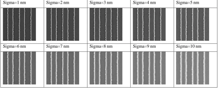
In this part we create synthetic images using a synthetic SEM image simulator, then added Gaussian blur with different sigma between 0 and 10 nm. The impact of the different blur values is shown in Figure 15 : Synthetic images with different associated blur values
Sigma=1 nm Sigma=2 nm Sigma=3 nm Sigma=4 nm Sigma=5 nm
Sigma=6 nm Sigma=7 nm Sigma=8 nm Sigma=9 nm Sigma=10 nm
Figure 15 : Synthetic images with different associated blur values
The different cross-section profiles for a couple of lines for the different synthetic images are illustrated in Figure 16. When increasing the amount of blur on the image, the left and right SEM signal peaks merge progressively.
13
Figure 16 : Profile view of the synthetic image with different levels of blur applied (sigma = 0nm to 10nm)
Thanks to the added information of the synthetic blur, it is possible to evaluate the MTFs as a function of level of blur and see the cutoff frequency behavior. Notice that, as expected, the cutoff frequency goes down as a higher blur levels is applied.
(a) (b)
Figure 17 : (a) MTF for the different blur configuration and (b) the cutoff frequency for each of the blur configurations According to Figure 17 (a) for high blur, there is a certain frequency zone which is hidden, when compared to lower blur. From the MTF we calculate the cutoff frequency or (cutoff wavelength) (Figure 17). According to the two tables there is a significant reduction in cutoff frequency from 0.02 𝑛𝑚−1 (25 nm in wavelength) between high and low blur conditions.
14
Figure 18 : LER measurement according to Blur
According to the Figure 18 This turns into a measurement difference of 20% in LER roughness.
5. CONCLUSION
The relative impact of the roughness to the behavior of integrated circuits is increasing as the technology advances. Techniques for assessing the roughness value have been proposed and improved over the years, mostly based on CD-SEM images. The CD-CD-SEM acquisition conditions also play a role in the perceived roughness, mainly acting as a low-pass filter. Being able to understand this phenomenon, evaluating if a measured PSD is reliable and identifying which acquisition conditions are best suitable depending on the type of roughness expected are some of the aspects covered in this paper.
Thanks to the demonstrated fidelity of synthetic data, it was possible to split the contribution of the different elements of the PSD extraction flow as well as it was possible to forecast the influence of the different acquisition conditions on the roughness measurements. This impact may be extended to other factors, such as the contour extraction algorithm [9]. We can also forecast if a given roughness is completely measurable or not as well as estimate the roughness measurement error (if present).
REFERENCES
[1] Constantoudis, V., Gogolides, E. and Patsis, G. P., “Line width roughness effects on device performance: the role of the gate width design,” Design for Manufacturability through Design-Process Integration IV, M. L. Rieger and J. Thiele, Eds., SPIE (2010).
[2] Azarnouche, L., Pargon, E., Menguelti, K., Fouchier, M., Fuard, D., Gouraud, P., Verove, C. and Joubert, O., “Unbiased line width roughness measurements with critical dimension scanning electron microscopy and critical dimension atomic force microscopy,” Journal of Applied Physics 111(8), 084318 (2012).
[3] Moussa, A., Lorusso, G. F., Sutani, T., Rutigliani, V., van Roey, F., Mack, C. A., Naulleau, P., Constantoudis, V., Ikota, M., Ishimoto, T., Koshihara, S. and Charley, A.-L., “The need for LWR metrology standardization: the imec roughness protocol,” Metrology, Inspection, and Process Control for Microlithography XXXII, O. Adan and V. A. Ukraintsev, Eds., SPIE (2018).
[4] Lorusso, G. F., Rutigliani, V., Van Roey, F. and Mack, C. A., “Unbiased roughness measurements: Subtracting out SEM effects, part 2,” Journal of Vacuum Science & Technology B 36(6), 06J503 (2018).
15
[5] Le-Gratiet, B., Bouyssou, R., Ducote, J., Ostrovsky, A., Beylier, C., Gardin, C., Schuch, N. G., Annezo, V., Schneider, L., Millequant, M., Petroni, P., Figueiro, T. and Schiavone, P., “Contour based metrology: “make measurable what is not so",” Metrology, Inspection, and Process Control for Microlithography XXXIV, O. Adan and J. C. Robinson, Eds., SPIE (2020).
[6] Babin, S., Calafiore, G., Peroz, C., Conley, R., Bouet, N., Cabrini, S., Chan, E., Lacey, I., McKinney, W. R., Yashchuk, V. V. and Vladar, A. E., “1.5 nm fabrication of test patterns for characterization of metrological systems,” Journal of Vacuum Science & Technology B, Nanotechnology and Microelectronics: Materials, Processing, Measurement, and Phenomena 33(6), 06FL01 (2015).
[7] Chris A. Mack, "Generating random rough edges, surfaces, and volumes", Applied Optics, Vol. 52, No. 7 (1 March 2013) pp. 1472-1480
[8] J. C. Novarini and J. W. Caruthers, “Numerical modelling of acoustic wave scattering from randomly rough surfaces: an image model,” J. Acoust. Soc. Am. 53, 876–884 (1973).
[9] Chris A. Mack, " Comparing edge detection algorithms: their impact on unbiased roughness measurement precision and accuracy", Proc SPIE Vol. 11325 (2020).