Controlled Growth and Doping of Core-shell GaAs-based Nanowires
byMichael Joseph Tambe B.S. in Creative Studies
University of California, Santa Barbara, 2005
Submitted to the Department of Materials Science and Engineering in Partial Fulfillment of the Requirements for the Degree of
ASSACHUSS INSTTUTE OF TECHNOLOGY
JUN
16 2010
LIBRARIES
ARCHNES
Doctor of Philosophy in Electronic Materials at the
Massachusetts Institute of Technology June 2010
C 2010 Massachusetts Institute of Technology. All rights reserved
Signature of Author:
Certified by:
Department of Ma'ferials Science and ngineering May 21, 2010
/24/ zfo
Silvija Grade'ak Merton C. Flemmings Assistant Pyfer of M 1s Science and Engineering
i7Thesis Supervisor
Accepted by:
Christine Ortiz Chair, Departmental Committee on Graduate Students
Controlled Growth and Doping of Core-shell GaAs-based Nanowires
byMichael Joseph Tambe
Submitted to the Department of Materials Science and Engineering on May 21, 2010, in Partial Fulfillment of the Requirements for the Degree
of Doctor of Philosophy in Electronic Materials ABSTRACT
The use of compound semiconductor heterostructures to create electron confinement has enabled the highest frequency and lowest noise semiconductor electronics in existence. Modem technology uses two-dimensional electron gasses and there is considerable interest to explore one-dimensional electron confinement. This thesis develops the materials science toolkit needed to fabricate, characterize, and control the compositional, structural and electronic properties of core-shell GaAs/AlGaAs nanowires towards studying quasi-one-dimensional confinement and developing high mobility electronics
First, nanowire growth kinetics were studied to optimize nanowire morphology.
Variations in nanowire diameter were eliminated by understanding the role Ga adatom diffusion on sidewall deposition and vertical growth was enabled by understanding the importance of Ga and As mass-transport to nanowire nucleation. These results demonstrate that arrays of
vertically-aligned GaAs nanowires can be produced. Then, the deposition of epitaxial AlGaAs shells on GaAs nanowires was demonstrated. By reducing the nanowire aerial density the stability of the nanowire geometry was maintained. A variety of analytical electron microscopy techniques confirmed the shell deposition to be uniform, epitaxial, defect-free, and nearly atomic sharp. These results demonstrate that core-shell nanowires possess a core-shell interface free of many of the imperfections that lithographically-defined nanowires possess.
Finally, the adverse effect of the Au seed nanoparticle during n-type doping was identified and n-type doping was achieved via the removal of the Au nanoparticle prior to doping. A combination of energy dispersive X-ray spectroscopy, current-voltage, capacitance-voltage, and Kelvin probe force microscopy demonstrated that if the Au seed nanoparticle is present during the shell deposition, Au diffuses from the seed nanoparticle and creates a rectifying IV behavior. A process was presented to remove the Au nanoparticle prior to shell deposition and was shown to produce uniform n-type doping. The conductivity of GaAs/n-GaAs nanowires was calculated as a function of donor concentration and geometric factors taking into account the effects of Fermi level pinning. The control demonstrated over all of these parameters is sufficient enough for core-shell nanowires to be considered candidates for high mobility electronics.
Thesis Supervisor: Silvija Gradecak
Table of Contents
List of Figures ... 9
List of Tables ... 15
Acknowledgements ... ,... 17
Chapter 1. Introduction and Motivation ... 19
1.1 A problem with scientific and technological interest ... 19
1.2 The semiconductor nanowire for high mobility electronics ... 20
1.3 Outline of thesis topic and work ... 22
Chapter 2. Background & Experimental... 25
2.1 N anow ire fabrication ... 25
2.1.1 Preparation of GaAs substrates for nanoparticle deposition... 27
2.1.2 Deposition of gold on GaAs substrates... 29
2.1.3 Metal-organic chemical vapor deposition... 30
2.1.4 Growth of core-shell nanowires by MOCVD... 34
2.2 Electron microscopy characterization... 35
2.2.1 Electron microscopy sample preparation... 36
2.2.2 Scanning electron microscopy theory and techniques ... 38
2.2.3 Transmission Electron Microscopy ... 39
2.2.4 Energy Dispersive X-Ray Spectroscopy... 43
2.3 Nanowire Electrical Characterization... 44
2.3.1 Preparation of characterization grids ... 44
2.3.2 Fabrication of contacts on individual nanowires ... 46
2.3.4 Kelvin probe force microscopy... 53
Chapter 3. Controlled growth of vertically aligned GaAs nanowire arrays ... 55
3.1 Demonstration of nanowire growth ... 55
3.1.1 Nanowire growth mechanism ... 55
3.1.2 Demonstration of GaAs nanowires... 57
3.1.3 Metrics of nanowire morphology... 59
3.2 Preparation of Au nanoparticles to control radius and position... 60
3.2.1 Deposition of gold from colloidal solution... 61
3.2.2 Au nanoparticle arrays by lithography and galvanic reaction ... 63
3.3 Optimizing growth temperature... 65
3.3.1 Preventing variation in nanowire diameter ... 65
3.3.2 Structural properties of GaAs nanowires... 67
3.3.3 Kinetic model explaining temperature effect... 67
3.4 Maximizing probability of vertical growth... 71
3.4.1 Effect of substrate orientation... 71
3.4.2 Effect of total group-III flow rate ... 73
3.4.3 Kinetic model for nanowire nucleation... 76
3.5 Optimized vertical GaAs nanowire arrays... 80
Chapter 4. Growth and properties of core-shell GaAs/AlGaAs nanowires... 85
4.1 Realizing epitaxial shell deposition ... 85
4.1.1 Shell deposition process... 86
4.1.2 High temperature stability of nanowires... 87
4.2 Composition of core-shell nanowires ... 92
4.2.1 Energy dispersive X-ray spectroscopy measurement ... 92
4.2.2 Modeling EDX compositional profiles... 93
4.2.3 Quantification of core-shell nanowire composition... 94
4.3 Morphological & compositional uniformity of core-shell nanowires ... 96
4.3.1 Axial uniformity of core-shell nanowires ... 96
4.3.2 Radial uniformity of core-shell nanowires ... 97
4.3.3 3D reconstruction of core-shell nanowires ... 98
4.3.4 Effect of shell deposition conditions on uniformity ... 99
4.4 Structural properties of core-shell nanowires ... 102
4.4.1 Structural analysis along nanowire length ... 102
4.4.2 Characterization of core-shell interface ... 104
4 .5 Sum m ary ... 106
Chapter 5. N-type doping of GaAs nanowires by the deposition of an n-GaAs shell .... 109
5.1 Nanowire Electronic Properties ... 109
5.1.1 A review of nanowire doping ... 109
5.1.2 Shell doping process ... I11 5.1.3 IV properties of undoped GaAs nanowires... 112
5.1.4 Determination of growth conditions ... 113
5.2 The adverse effect of Au on n-type doping ... 116
5.2.1 Unintended electrical rectification in nanowires ... 116
5.2.2 Characterization of rectification & estimation of band structure... 118
5.2.4 D iscu ssion ... 124
5.3 Realization of n-type GaAs nanowires via Au removal ... 127
5.3.1 Electrical properties of Au-removed doped shell nanowires... 128
5.3.2 Predictive model for the conductivity of n-GaAs nanowires... 132
5.4 C onclusions... 136
Chapter 6. Conclusions... 139
6.1 Research impact & suggested future directions... 141
Appendix A: Matlab code for core-shell EDX modeling ... 145
Appendix B: Igor code for nanowire mapping ... 147
List of Abbreviations ... 149
List of Figures
Figure 2-1: The galvanic reaction to deposit Au on GaAs. 1) A patterned substrate is immersed in Au+3 solution. 2) Au+3 ions replace Ga+3 and As+3 ions producing oxides. 3) PMMA is
removed. 4) GaAs nanowires are grown by MOCVD... 30 Figure 2-2: a) Schematic of MOCVD reaction chamber. b) Picture of chamber during operation. ... 3 2 Figure 2-3: Schematic showing the various kinetic steps in MOCVD growth. Steps in blue are categorized as gas-phase mass transport limited steps and steps in red are categorized as
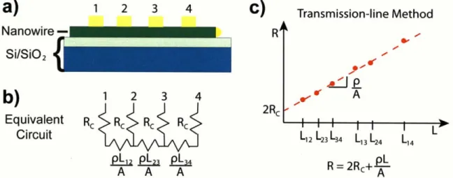
kinetically-limited steps. Adapted from [49]... 33 Figure 2-4: Plot of the temperature (left axis) and precursor flow (right axis) profile during a typical core-shell nanow ire grow th... 34 Figure 2-5: Schematic of the various signals that can be produced and collected in an electron microscope. All images have scale bar equal to 100nm. Adapted from [52]. ... 36 Figure 2-6: Schematic showing the preparation process for plan-view and cross-section nanowire T E M sam p les. ... 38 Figure 2-7: HAADF STEM images and corresponding Fourier transforms taken on the same sample a) with and b) without carbon coating ... 43 Figure 2-8: Schematic of contacting process showing sonication of nanowires into suspension, deposition of nanowires on the grid, and deposition of contacts... 48 Figure 2-9: a) Schematic of thin film sheet resistance measurement using the Van der Pauw m ethod. b) Expected IV curve ... 50
Figure 2-10: a) Schematic of nanowire two-point measurement. b) Expected IV curve and
physical m eaning of m easured resistance ... 51
Figure 2-11: Transmission line method measurement on single nanowire. a) Schematic of
contacted nanowire. b) Equivalent linear circuit. c) Plot of resistance versus length. ... 51 Figure 2-12: Schematic of Kelvin probe force microscopy measurement. ... 54
Figure 3-1: Schematic showing the steps of GaAs nanowires by the Au assisted vapor-liquid solid m echanism ... 56 Figure 3-2: a) SEM images of Au nanoparticles resulting from a 6A Au film annealed at 600C. b) Histogram of nanoparticle diameters, after annealing at 600"C, taken from many SEM images. ... 5 8 Figure 3-3: a) SEM image of dense forest of VLS-grown nanowires. b) EDX spectrum proving GaAs composition. c) SEM image of a lone nanowire showing tapered morphology... 59 Figure 3-4: Schematic of a vertical GaAs nanowire showing the morphology metrics... 60 Figure 3-5: Diameter distributions of Au nanoparticles on GaAs 111 B substrates at different aerial catalyst densities after annealing at 600'C for 10 min. The left and right histograms show the same data over different diameter ranges. ... 62 Figure 3-6: a) SEM image of nanoparticles arrays prepared using electron-beam lithography and galvanic reaction after annealing at 600'C for 10 min. Inset is AFM image with height profile. The distribution of nanoparticle positions relative to the mask are shown b) before and c)
annealing at 600'C for 10 m in... 64 Figure 3-7: TEM images of nanowires grown at 420C (a) and 480C (b)... 66
Figure 3-8: The tapering factor plotted on an Arrhenius plot showing shell deposition is a
thermally-activated process with activation energy of 56 kcal/mol. ... 66 Figure 3-9: High resolution TEM image of a GaAs nanowire grown at 420'C. b) Bright-field TEM image of twinning in a nanowire grown at 480'C... 67 Figure 3-10: Schematic showing the pathways for TMG and how excess Ga adatoms can create radial grow th in nanow ires... 68 Figure 3-11: Planview SEM images of GaAs nanowires grown on a) GaAs 100 and b) GaAs
111 B substrates with observed texturing in inset. ... 72 Figure 3-12: Bright-field TEM of GaAs nanowire with SAD pattern, (01-1) zone axis... 72 Figure 3-13: Tilted SEM images of GaAs nanowire grown at a) TMGa flow = 2.0 sccm and b) TMGa flow = 0.3 sccm with V/III ratio constant. c) The vertical percentage versus flow rate... 74 Figure 3-14: Phase diagram for the a) Au-Ga system and b) Au-As system... 75 Figure 3-15: a) Schematic of Ga-limited nucleation with corresponding SEM image showing vertical growth. b) Schematic of As-limited nucleation, with corresponding SEM image showing non-vertical grow th ... 77 Figure 3-16: Growth rate calculation for GaAs nanowire growth... 81 Figure 3-17: a) SEM image of an optimized vertical GaAs nanowire array. Distributions of the b) positions, c) diameters, and d) heights the nanowires grown from the Au nanoparticle array show n in F igure 3-6. ... 82 Figure 4-1: Schematic showing the shell deposition process. ... 87
Figure 4-2: SEM micrographs of GaAs/AlGaAs nanowires a) dense nanowire grown at 650'C showing morphological instability, inset is sample at lower magnification and b) sparse nanowire grown at 700'C maintaining morphological stability... 88 Figure 4-3: SEM micrographs of vertical core-shell nanowires showing a) 80 -90% of nanowires maintain a stable morphology and b) the shell is faceted with a hexagonal cross-section... 90 Figure 4-4: a) Histogram of nanowire diameter before and after shell deposition as well as TEM micrographs of nanowires b) before and c) after shell deposition... 91 Figure 4-5: a) EDX spectra of a nanowire core and a core-shell nanowire. Signal normalized for As K line. b) Ga and As EDX profiles across the diameter of a core-shell nanowire. Inset is
STEM im age of core-shell nanow ire... 92 Figure 4-6: Height profile for a hexagonal cross-section nanowire resting on a) a facet corner and b ) on a facet... 94 Figure 4-7: EDX profiles for Ga and Al signals in core-shell plotted alongside Gaussian beam broadening model for a core-shell nanowire a) laying on a facet corner and b) laying on a facet sid ew all. ... 9 5 Figure 4-8: The shell composition and thickness of a representative core-shell nanowire
measured by EDX at different point along the length of the nanowire. ... 97 Figure 4-9: High angular annular dark field STEM image of core-shell nanowire cross-section and corresponding chemical maps for aluminum, gallium, and arsenic... 98 Figure 4-10: a) HAADF STEM images of core-shell nanowires taken at different angles. b) 3D reconstruction of a core-shell nanowire imaged using HAADF STEM tomography. Images courtesy of Dr. Peter Cherns, CEA Grenoble... 99
Figure 4-11: Basic zone diagram for shell deposition. ... 100 Figure 4-12: a) Bright field TEM micrograph of a core-shell nanowire. Inset is selected area diffraction pattern along <110> direction. b) Lattice-resolved TEM micrograph of GaAs/AlGaAs interface between the GaAs nanowire and the Au seed nanoparticle. Inset is same image at lower magnification showing relative positions of GaAs, AlGaAs, and Au... 103 Figure 4-13: a) Lattice-resolve high angular annular dark field STEM image of core-shell
interface in cross-section with Fourier transform in inset and b) STEM intensity profile of the core-shell interface along the dashed line in (a). Blue dashed line denotes interfacial region... 105 Figure 5-1: Schem atic of shell doping process... 111 Figure 5-2: Transmission line method measurement of nanowire resistance... 112 Figure 5-3: Secondary Ion Mass Spectroscopy data for n-GaAs/n-AlGaAs thin-film growth a) 700'C and b) 750'C ... 114 Figure 5-4: Direct current IV data for a) a GaAs (100) control sample and b) a representative GaAs/n-GaAs core-shell nanowire with false-colored SEM of shell contacted nanowire... 116 Figure 5-5: Electrical characterization between contacts A & B showing a) direct-current I-V behavior and b) C-V profiling using an AC bias of 500 mV at 1kHz. Inset is same data in a different voltage region and scaled accordingly... 119 Figure 5-6: Proposed band structure of GaAs/n-GaAs nanowire between contacts A and B. ... 120 Figure 5-7: Kelvin probe force microscopy of a representative nanowire along the dotted green line pictured in the corresponding SEM image. The red diamonds with connecting line are measured Kelvin potential, normalized to value of the Au nanoparticle and the blue dashed line is the nanow ire height profile. ... 122
Figure 5-8: a) EDX profiles of Ga, As, & Au at the Au-GaAs interface. Inset is STEM image with linescan shown as the green dashed line b) Comparison of Au EDX signal in a doped shell versus undoped nanowire. The signals were normalized to their maximum Au count. ... 124 Figure 5-9: Proposed models for rectification. a) Au diffusion creates midgap states with
observed rectification between Si- and Au-doped segments. b) Au diffusion creates degenerately p-doped region with observed rectification between the n-GaAs and diode depletion region... 126 Figure 5-10: Schematic of modified shell doping process including TFA etching process... 128 Figure 5-11: a) DC IV measurement of a representative shell-doped nanowire and b) TLM measurement of resistance versus length. Inset is false-colored SEM of contacted nanowire... 129 Figure 5-12: a) TLM determination of nanowire and contact resistance and b) back gated IV of the nanowire shown in Figure 5-11 between A-B showing n-type conduction. Error bars are difference between forward and reverse sweep opf source-drain voltage... 130 Figure 5-13: a) Schematic of effect of Fermi level pinning on free electron density, and b)
thickness of surface depletion layer at different donor concentrations... 133 Figure 5-14: Simulated conductivity of core-shell GaAs/n-GaAs nanowires at different shell thickness and carrier concentrations assuming core radius = 50 nm and t = 2000 cm2/V-s.... 135 Figure 6-1: Band diagram and proposed structure of core-shell GaAs/AlGaAs structure. ... 142 Figure 6-2: Schematic of nanowires embedded in organic materials for a solar cell... 143
List of Tables
Table 3-1: The percentage of nanoparticles that undergo a merging event as a function of initial nanoparticle aerial density. ... 63 Table 3-2: Optimized growth parameters for vertical GaAs nanowire growth ... 80
Acknowledgements
I would foremost like to thank my advisor, Professor Silvija Grade'ak. She took a real risk accepting me as her first student. When looking for a student to help establish an
experimental lab, choosing someone with virtually no experimental experience is not the obvious choice. Throughout my PhD, she managed to simultaneously be demanding, empathetic, and supportive. I've never figured out quite how she manages this complex balance, but I'm quite sure it stems from her vast repertoire of nuanced facial expressions. She is a great teacher and a great researcher, a truly rare combination. I could not have asked for a better advisor. Any
success I have in life, I will owe to her fostering my sense of leadership and independence. I only regret never learning the proper way to pronounce the "C" in Grade'ak. I would also like to thank Professor Gene Fitzgerald for practically adopting me into his group and instilling in me a skeptic's eye when viewing technology. Any success I may have in business, I owe to his guidance and endless supply of anecdotes. I would like to thank Professor Tomas Palacios for his device expertise and indomitable enthusiasm. It definitely helped me down the long dark tunnel of the PhD and almost made me wish I worked on gallium nitride.
I would also like to thank my fellow graduate students. First, I'd like to thank Steve Boles for helping to kickstart my research, teaching me about the "joys" of MOCVD, and always being around to bounce an idea off. I'd like to thank Sung Keun Lim for patiently teaching me TEM, hanging out, and drinking me under the table. I'd like to thank Matt Smith for sharing my doping pain and helping me fight through it with a well-timed joke. I'd like to thank Mayank Bulsara and Arthur Pitera for always helping me fix that stupid 5th floor lab and giving me the confidence
to stay calm in a panic situation. If someone someday runs into my office yelling "The building is on fire" and my response is "Not now, I'm busy", I'll owe it you. I'd like to thank Megan
Brewster for teaching me to carpe diem. I've never met someone who can create so many opportunities for herself and hope I can learn just a little bit of that skill. To Shih-wei Chang and Nan Yang, I thank you for your never-ending supply of witty remarks. To Dana Shemuly and Yoda Patta, I thank you for always caring. To Sam, Eric, and Jordan, and Xiang, I wish you luck with your studies.
I would also like to thank the various research staff I've worked with. I'd like to thank Dr. Tony Garratt-Reed. Despite your best efforts you did not just teach me how to use the microscopes, you taught me how to be a microscopist or at least impersonate one. To Kurt Broderick, I will never understand how I am getting a PhD from MIT and you don't have one. You are a true lab MacGyver and I'll be sure to call you if I ever need to build a build a nuclear reactor from a rod of uranium, the spare parts from a sputterer, some rubber bands and a paper clip. To Yong Zhang, Mark Mondol, Ellen Lavoie, Patrick Boisvert, Dave Terry, and Dennis Ward thanks for all you advice and assistance. I'd also like to thank the various other professors who have helped me. To Professor Nicola Marzari, thanks for providing an amusing
non-sequitor perspective on life; let me know when Stockholm calls. To Professor Craig Carter,
thanks for modeling advice and an endless stream of pointless but amusing conversations about such topics as how to fart at OK. I still maintain that it is possible, but you wouldn't smell it.
Last, but not least, I'd like to thank my family and my girlfriend Stephanie. To my parents, thanks for instilling in me the values of hard work, honestly, and respect. Thanks for supporting me, catching me when I fell, and encouraging me to take a break from my work. To Stephanie, I couldn't have asked for a better companion to guide me through the trails and tribulations of grad life. Thanks for supporting me, comforting me when I was frustrated, and forcing me to take a break from my work.
Chapter 1.
Introduction and Motivation
Nanotechnology, the study and practical application of the unique properties of the nanoscale, holds great promise for improved performance and novel functionality in devices. One device that already utilizes the unique properties of the nanoscale is the high electron mobility transistor. By confining electrons to two dimensions, transistors with increased frequency response and lower noise have been produced and form the foundation of modern mobile telecommunications. Recently demonstrated
quasi-one-dimension semiconductor structures, nanowires, may be able to confine electrons to one dimension expanding current understanding of electronic conduction and provide a platform for future high mobility devices. This thesis develops the materials science toolkit needed to fabricate, characterize, and control the compositional, structural and electronic properties of core-shell GaAs/AlGaAs nanowires towards studying quasi-one-dimensional confinement and developing high mobility electronics
1.1
A problem with scientific and technological interest
Beginning with Richard Feynman's vision in 1959 [1] and bolstered by the
unprecedented scientific, technological, and societal advancements that the microelectronics industry created, the notion of controlling matter down to the nanometer scale has generated substantial interest from both scientists and technologists. For the scientist, nanostructures allow the study of the atomistic mechanisms controlling materials properties in an unprecedented way. For the engineer, nanostructures present the ultimate building blocks to create devices with improved performance or novel functionality. This convergence of scientific and technological interest has led many to predict that the study of materials at the nanometer scale, commonly referred to as nanotechnology, is the next great frontier of scientific advancement and economic growth [2].
The belief that a field with both scientific and technological interest is a breeding ground for novel technology has precedent. Consider the development of the high electron mobility transistor. Band theory predicts that creating a heterointerface between two materials with different bandgaps creates an energy potential well. This energy well creates electron
confinement, which enhances carrier mobility by suppressing vibrational scattering mechanisms. The belief that epitaxial heterostructures could lead to improved performance electronics
generated both scientific and technological interest. When the ability to epitaxially grow thin films of GaAs/AlGaAs with exceptionally low defect densities was developed in the 1960's, scientists were able to experimentally study the effect of reduced dimensionality on electron conduction. They confirmed the presence of two-dimensional free electron gas (2D FEG) and also found that the conduction band offset was able to trap free carriers from a doped layer many tens of nanometers away from the heterointerface. This effect, known as modulation doping [3], enabled a transistor with electron mobility twice that of its doped counterpart [4] creating electronics with higher frequency response and lower noise than any other semiconductor technology.
Nanotechnology may hold the key to continuing advancement in high mobility
electronics. To extend the study of reduced dimensionality on electron conduction from 2D to 1D requires the ability to produce quasi one-dimensional single crystalline heterostructures that support transport of charge carriers along their length while maintaining nanoscale effects across their diameter. This structure is referred to as a semiconductor nanowire.
1.2
The semiconductor nanowire for high mobility electronics
There exist two fundamentally different approaches to fabricate nanowires. The first approach to producing nanowires is the top-down approach. Top-down nanowires are produced by carving out a nanowire from a piece of bulk semiconductor material using lithography and etching. This approach utilizes the mature fabrication technology of the semiconductor industry allowing for easier integration with current CMOS technology. However, the top-down approach suffers many of the same materials quality issues inherent to lithography and etching, such as
surface roughness and surface traps. Attempts to create one-dimensional conduction with top-down nanowires failed because the surface roughness inherent to this fabrication method
produced additional scattering centers [5]. So while top-down nanowires may be useful for near-term applications in integrated circuits [6], top-down nanowires are unsuitable as a platform for continued advancement in high mobility electronics.
The second approach to producing nanowires is the bottom-up approach. Bottom-up nanowires are produced by inducing single-crystalline semiconductor growth in a nanowire shape. Since the nanowire structure is produced by epitaxial crystal growth, bottom-up nanowires have shown heterointerfaces with the same crystalline quality as MODFETs both perpendicular and parallel to the substrate orientation [7, 8]. As a result, bottom-up nanowires are ideally suited as a platform to study the effect of reduced dimensionality of electron [9, 10] and phonon [11, 12] conduction. There exist various methods to produce bottom-up nanowires such as selective area epitaxy [13] and solution-liquid-solid growth [14], but the most widely studied method is the Au-mediated vapor-liquid-solid (VLS) mechanism [15], which has been shown to produce GaAs nanowires [16, 17] as well as proof-of-concept transistors [18-24], light
emitting diodes (LEDs) [25], lasers [26-28], and photovoltaics [29, 30].
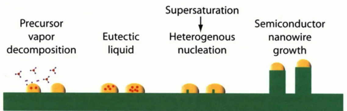
Au-mediated VLS nanowire growth utilizes a seed Au nanoparticle as a preferential decomposition site for gallium precursor and creates a driving force for the heterogeneous nucleation of a quasi-one-dimensional single crystal of GaAs. The GaAs/AlGaAs material system is an ideal system to study quasi-one-dimensional conduction since the GaAs/AlGaAs system has only 0.13% misfit enabling heterointerfaces with low defect densities and bulk GaAs exhibits electron mobilities as high as 8500 cm2/V-s at room temperature.
1.3
Outline of thesis topic and work
In order to study quasi-one-dimensional conduction in GaAs/AlGaAs nanowires towards high mobility applications, a materials science toolkit is first needed to fabricate an appropriate test structure. A method to produce GaAs nanowires must be demonstrated with control over nanowire morphology and structure. Once GaAs nanowire growth is understood, the deposition
of an epitaxial AlGaAs shell deposition must be demonstrated. In order to ensure an epitaxial heterointerface capable of producing quasi-one-dimensional confinement, the structural and core-shell interfacial properties must be characterized and deemed to be free of imperfections that add additional scattering centers. Finally, the electronic properties of core-shell nanowires must be understood and methods devised to provide controllable doping.
Prior to this thesis work had been done to fabricate core-shell GaAs/AlGaAs nanowires, however the morphology of these structures were not controlled, the nanowire structural and core-shell interfacial properties were not known, and n-type doping in GaAs nanowires had not been achieved [31-35]. This thesis studied the growth and properties of core-shell GaAs/AlGaAs nanowire heterostructures and accomplished the following three objectives. First it demonstrated the ability to fabricate uniform vertically-aligned GaAs/AlGaAs nanowires. Second, the
structural, compositional, and core-shell interfacial properties of GaAs/AlGaAs nanowires were characterized and shown to be defect-free, uniform and nearly atomically sharp, respectively. Third, the adverse effect of the Au seed nanoparticle was understood and overcome yielding uniform n-type shell doped GaAs nanowires. This work creates the materials science toolkit to use n-type doped core-shell GaAs/AlGaAs nanowires to study reduced dimensionality on electronic conduction and develop core-shell nanowire electronics.
The thesis is organized in six chapters, as follows. Chapter 2 explains in detail the experimental methods and protocols utilized to fabricate and characterize nanowires [36]. The reader is directed to read this chapter if interested in the specific details of the experiments used to prove the results presented in Chapters 3 through 5. Chapter 3 presents studies on fabricating uniform vertically-aligned arrays of GaAs nanowires. The growth kinetics of nanowires were understood and optimized to control nanowire morphology [37]. These results demonstrate that arrays of vertically-align GaAs nanowires can be produced, making them viable candidates for integrated device applications [38]. Chapter 4 presents studies exploring the deposition and characterization of AlGaAs shells on GaAs nanowires. These results demonstrate that the morphology, composition, and crystalline quality of core-shell nanowires can be controlled precisely enough for applications in high mobility electronics [39]. Chapter 5 presents studies on n-type doping via the deposition of a doped shell. These results highlighted the adverse effect of the Au seed nanoparticle and demonstrated that doping can be achieved in radial heterostructures [40]. Finally, Chapter 6 summarizes the results and provides insight and opinions on the future of core-shell GaAs/AlGaAs nanowire research for high mobility applications.
Chapter 2.
Background & Experimental
The purpose of this chapter is to introduce the various experimental techniques used in this thesis. First, the metal-organic chemical vapor deposition technique used for the growth of nanowire is presented, including a discussion of reactor design and reaction chemistry. Second, the electron microscopy techniques used to investigate the structural, compositional, and core-shell interfacial properties core-shell nanowires are presented. This includes a discussion of scanning electron microscopy, transmission electron microscopy, scanning transmission electron microscopy, and energy dispersive X-ray spectroscopy. Finally, the processing and measurement techniques used to
investigate the electrical properties of individual nanowires are presented, including a discussion of depositing contacts on individual nanowires, electrical measurement techniques, and Kelvin probe force microscopy.
2.1
Nanowire fabrication
As explained in Chapter 1 this thesis will study the epitaxial growth of bottom-up GaAs/AlGaAs core-shell nanowires. Inducing epitaxial growth in the nanowire geometry has two requirements. First, a substrate preparation process must be developed to only permit nucleation and growth on predefined areas of a substrate. Second, growth conditions must be engineered to create kinetic barriers to crystal growth in all but one direction. Two growth mechanisms have been shown to produce epitaxial nanowires: metal-free selective area epitaxy (SAE) and the metal nanoparticle mediated vapor-liquid-solid (VLS) growth mechanism.
SAE growth of GaAs nanowires was first reported by Fukui in 1991 [13]. The nucleation sites are defined by creating nanoscale pores in a silicon dioxide mask atop a GaAs (11 1)B substrate using lithography. The sample is then inserted into a metal-organic chemical vapor deposition chamber and grown under carefully designed conditions to promote selective growth in the <l11> direction. This method has been shown to produce uniform arrays of GaAs
nanowires and is a promising approach for future commercial devices based on GaAs nanowires. However, SAE has not been shown able to produce nanowires with diameters less than 60 nm
[41] due to lack of clear facet formation at low diameters. This would prevent the study of electron conduction at important quantum mechanical length scales.
To achieve smaller diameters, the use of a metal nanoparticle to seed the nanowire growth is required. The VLS mechanism utilizes a metal nanoparticle to act as a gettering source for the gallium and arsenic source material and the solubility limit of GaAs in the metal
nanoparticle to induce phase separation of the GaAs from the metal nanoparticle. This method has been shown with CMOS compatible metals such as Mn [42], however nanowire growth experiences kinking and structural defects. On the other hand, VLS nanowires grown using Au as the seed nanoparticle have shown GaAs nanowire growth free of kinking and structural defects [16], making it ideal for the fabrication of a test structure to study lower dimensional conduction. If studies on Au-grown nanowires reveal that GaAs/AlGaAs nanowires may be viable candidates for commercial applications, then nanowire growth using a CMOS-compatible metal or SAE can be explored.
Nanowires have been demonstrated using a variety of growth systems including
conventional III-V growth techniques such metal-organic chemical vapor deposition (MOCVD) [13] and molecular beam epitaxy [43]. For thin-film electronics, MBE is known to achieve higher purity films and is commonly used to prototype a device, whereas metal-organic chemical vapor deposition can achieve commercial-scale throughput and is used demonstrate process scalability and compatibility with commercial techniques. It might seem logical to use MBE to produce a test structure to study quasi-i D conduction. However, VLS nanowire growth requires the creation of a kinetic barrier to growth in all but one direction. Since MOCVD growth
introduces reagent material in the form of chemical precursors, it allows for selective area epitaxy since metal nanoparticles can act as a preferential decomposition and nucleation site for
precursor. MBE introduces reagent material in elemental form, which means that reagent material can spontaneously react before reaching the Au nanoparticle. Hence MBE is less
desirable than MOCVD for VLS nanowire growth because it is less able to provide selective area nucleation and growth.
Fabricating nanowires by the Au mediated VLS mechanism is a three-step process. First GaAs wafers ready for epitaxial growth (epi-ready) were diced into smaller samples. To protect the epi-ready surface of the GaAs, a protective layer of silicon dioxide was deposited by plasma enhanced chemical vapor deposition prior to dicing. Once epi-ready die were prepared gold was deposited to seed nanowire growth and this section describes the three methods utilized to deposit Au nanoparticles: evaporation of a thin film, deposition of colloidal gold nanoparticles,
and galvanic reaction on a lithographic template. Once gold seed particles are on the substrate, nanowire growth is conducted by metal-organic chemical vapor deposition (MOCVD). This
section presents an overview of MOCVD theory as well as the growth conditions used for core-shell nanowire growth.
2.1.1
Preparation of GaAs substrates for nanoparticle deposition
Prior to further processing, GaAs substrates were coated with a layer of silicon dioxide and polymer to protect the top surface. Wafers were then cut with a die saw into squares and cleaned using solvents and oxygen plasma.
Nanowire growth substrates were prepared from 2" single-side polished GaAs wafers. Both (100) and (11 1)B substrates were used. GaAs (11 1)B substrates were used for vertical nanowire growth while GaAs (100) substrates were used since it is the orientation most often used in commercial applications. Small samples of the substrate were cut by use of a diesaw. For dicing, a 500nm thick protective silicon dioxide layer was deposited at 250*C using a Surface
Technology Systems plasma-enhanced chemical vapor deposition reactor. This layer ensured that no organic material or particulate matter came into contact with the polished surface. A second protective layer of PMMA A4 resist, was spin coated at 3000 rpm and soft baked on a hotplate at 180'C for 1.5 min. The final layer thickness was 400 nm. The resist was deposited to ensure the wafers did not cleave during dicing. Individual die were then cut 8mm by 8mm using a Disco Abrasive System Model DAD-2H/6T diesaw.
Prior to nanoparticle deposition, the substrates underwent cleaning to remove any organic contamination. The substrates underwent a 3-solvent cleaning procedure, followed by oxygen plasma cleaning. The 3-solvent clean consisted of ultrasonic cleaning in a bath of acetone (99.5% purity), methyl alcohol (99.8% purity), and then isopropyl alcohol (IPA) (99.5% purity) each for
10 min. After cleaning in isopropyl alcohol, the samples were blown dry in a nitrogen stream (99.9% purity). As a final clean, a Plasmod 4" barrel oxygen plasma cleaner operating at 100 W was used to clean the substrates for 10 min. Nanoparticle deposition took place within 30 min of plasma cleaning.
Substrates to be patterned by electron beam lithography were spin coated with PMMA 950K (1 wt% in anisole) purchased from Microchem, then soft baked on 180'C hotplate for 3 min before exposure. The thickness of the coated PMMA was about 50 nm measured by a KLA-Tencor P10 profilometer. The substrates were exposed on a Raith-150 scanning electron beam lithography (EBL) system at an accelerating voltage of 30 kV with a dot dose of 0.04 pA-s-cm-2.
The PMMA was developed in methylisobutylketone (50% in IPA) for 30 s at 21'C and then rinsed in IPA for 30 s. Lift-off was performed by immersing the samples in a
1,2-dichloroethane (DCE) solution [44] followed by 10 min of 02 plasma cleaning in a Plasmod 4" barrel oxygen plasma cleaner operating at 100W.
2.1.2
Deposition of gold on GaAs substrates
As mentioned above, gold was deposited by one of three methods: colloidal solution, thin film, or electron beam lithography with galvanic displacement. For deposition from colloidal solution, the surfaces of the GaAs growth substrates were made hydrophilic by deposition of poly-l-lysine solution (40mL). After 10 min, the substrates were then gently rinsed in stream of deionized (DI) water and dried in a stream of nitrogen (99.9% pure). Next, 40 mL of
commercially available colloidal gold solution with diameters ranging from 5 - 100 nm was dropped onto the substrate surface. The colloidal solution was left on the substrate for 5 -20 min to allow the colloids to precipitate on the substrate surface. The sample was then gently rinsed in stream of DI water and then gently blown dry in a stream of nitrogen gun (99.9% pure). For thin film gold deposition the GaAs growth substrates were inserted into a Sloan 8 kV electron beam evaporator. A thin film of gold was deposited at a background pressure of 3 x 10⁻⁶ torr and a deposition rate of 1A/s and the final film thickness was 0.6 -3.0 nm.
Finally for the galvanic displacement deposition, the Au+3 solutions were prepared by
dissolving hydrogen tetrachloroaurate (1II) trihydrate into deionized water. Prior to the galvanic reaction, the substrates were immersed in a 2% (v/v) aqueous hydrofluoric acid (HF) solution for 5 min to remove the native oxide layer. The growth substrates were patterned to provide
diameter- and position-controlled deposition of Au nanoparticles. The patterned GaAs 111 [B] substrates were patterned by EBL and then immersed in Au+3 solution of 5x
10-5 M for reaction time of 20 min.
The reaction is shown in Figure 2-1. Au+3 ions diffuse to the surface of the GaAs
substrate due to the concentration equilibrium effect. Once the Au*3 ions contact the surface directly, a spontaneous reduction occurs due to the difference in the standard reduction potential
(the Au+3 /Au pair, 1.42 V versus a normal hydrogen electrode (NHE), is higher than those of
Ga+3 /Ga, -0.56 V versus NHE, and the As*3/As pairs, 0.234 V versus NHE) [45]. The Au*3 ions receive reducing electrons from the bonding electrons of the GaAs substrate (valence band) [46] forming Au nanoparticles and producing gallium and arsenic oxide on the surface of the GaAs substrate. After the reaction, all the samples were thoroughly washed by DI water to remove the residual Au+3 ions.
Au+3
-solution~
,
1
U10PMMA
galvanic
etch
GaAs substrate reaction
substrate
3
PMMA
o
u
+rem
ovalo
AuO
4
Ga
2O
3Wnanowire
As
20
3growth
Figure 2-1: The galvanic reaction to deposit Au on GaAs. 1) A patterned substrate is immersed
in Au+3 solution. 2) Au.3 ions replace Ga+3 and As+3 ions producing oxides. 3) PMMA is
removed. 4) GaAs nanowires are grown by MOCVD
2.1.3
Metal-organic chemical vapor deposition
Metal-organic chemical vapor deposition is the commercial standard for epitaxial growth of single crystalline III-V semiconductors. It is highly scalable and capable of very high
throughput, unlike molecular beam epitaxy, and offers greater control over composition and purity than other methods such as hydride chemical vapor deposition or liquid phase deposition. Complete descriptions of MOCVD can be found elsewhere [47]. What follows is a general description of MOCVD operation and the key concepts required to understand the work presented in this thesis.
The process operates by introducing the growth elements from the vapor phase within a chemical compound known as a precursor. A combination of thermodynamics and fluid
dynamics creates a chemical potential difference that drives the precursors to the growth surface. Once there, a series of decomposition and deposition reactions occur. These reactions break down the precursor yielding the growth element, out-react the decomposition reaction by-products, and drive the crystal growth of the semiconductor material.
A metal-organic chemical vapor deposition reactor consists of two major subsystems: a gas delivery system and a reaction chamber. Each of the two subsystems independently controls one of the two primary process parameters of the growth. The gas delivery controls the partial pressure of the reagent gasses. This correlates directly to the amount of reagent supplied to the reactions. The reaction chamber controls the reaction temperature, which directly affects the reaction rates.
The gas delivery system is a network of valves and mass flow controllers designed to create a controlled mixture of carrier and precursor gasses flowing into the reaction chamber. Each precursor gas supplies an element of the material to be deposited contained within a chemical compound. The carrier gas is a constant flow of gas not containing a deposition material. The carrier gas stabilizes the flow of the gas mixture as the flow rate of the carrier gas is always greater than one hundred times the total flow of the precursors and kept constant throughout the process.
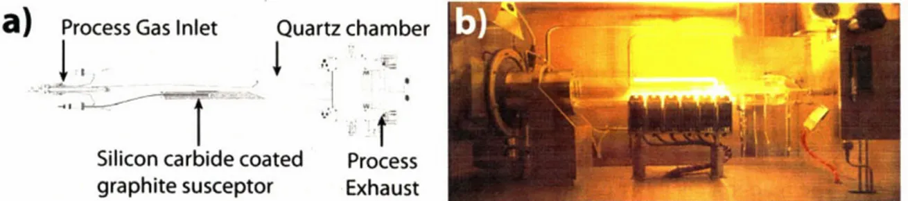
The reaction chamber is a heated chamber where the precursor gasses decompose and deposit material on the samples. In this thesis a horizontal reactor, as shown in Figure 2-2, was used. The chamber and all of its components are made from single crystalline quartz to operate at temperatures up to 8000C. The input gas is delivered from the gas delivery system into the
reactor. The inlet is designed to ensure the flow of gas is laminar and evenly distributed over the chamber. The samples are placed atop a graphite susceptor, which is indirectly heated by infrared lamps. The susceptor, with a much larger thermal mass than the samples', ensures the
temperature of the samples stays uniform. The indirect heating ensures that only the graphite susceptor is directly heated while the quartz chamber is not. This is known as a "cold-wall" configuration and is designed to ensure that the precursors primarily diffuse to and decompose on the samples and not on the quartz chamber.
a)
Process Gas Inlet Quartz chamberSilicon carbide coated Process graphite susceptor Exhaust
Figure 2-2: a) Schematic of MOCVD reaction chamber. b) Picture of chamber during operation. The deposition of material by MOCVD occurs via two distinct types of reactions:
decomposition and deposition. The reactions for GaAs are shown in Equation (2- 1).
Ga(CH,), + AsH, H2 >Ga+As+3H+3CH3 > GaAs+3CH4 (2-1)
The first reaction is the decomposition of the precursors to yield the desired deposition element. It should be noted that many sub-reactions occur and the decomposition reactions produce by-products that must diffuse away. Both of these facts can affect the growth kinetics of nanowires [48]. The second reaction is the deposition of material; this reaction is simply the elements supplied by the precursor incorporating into the lattice of the substrate. In this thesis, the composition of all deposition materials can be generalized as AlxGaixAs:Siy where x is the percentage of aluminum in the AlGaAs alloy and y is the doping level of silicon in the AlGaAs alloy.
2AB
(gas)-
2A (solid) + B2 (gas)i-on-o precursors Diffusion of by-products
- ABbulk (gas) B2 bulk (gas)
--AB surface (gas) i Deposition B2 surface(gas) Adsorption .LDesorption
-~~~ - - -.. ~ -.- - - - +I* + EI~-~r~aci~
DecomposiionAB*-+-*B* + A*---+LBB BB* Out-reaction
Figure 2-3: Schematic showing the various kinetic steps in MOCVD growth. Steps in blue are categorized as gas-phase mass transport limited steps and steps in red are categorized as
kinetically-limited steps. Adapted from [49]
Understanding how growth conditions will effect the composition of the material produced requires an understanding of the reaction kinetics. In general, there are a variety of different kinetic steps that occur in this process, as shown in Figure 2-3. The slowest one is referred to as the "rate-limiting step" and determines the overall reaction rate. These steps can be divided into two categories. The first category is gas-phase mass-transport, which includes the diffusion of precursor to the sample, the adsorption of the precursor onto the surface, the desorption of reaction by-products, and the out-diffusion of reaction by-products. If the rate limiting step is a gas-phase mass-transport step, then the parameters x and y in are determined by the relative flow rates of the precursor gasses and the total growth rate is determine by the total flow rate. The second category of kinetic steps is referred to as reaction steps, which includes precursor decomposition, material deposition, and the out-reaction of by-products. If the rate limiting step is a reaction step, then the parameters x and y as well as the growth rate are determined by the growth temperature. Since the temperature typically determines the crystallinity of the deposition material, it is undesirable to have a reaction step be the
rate-limiting step. MOCVD reactors are typically designed to operate such that a gas-phase mass transport step is the rate-limiting step.
2.1.4
Growth of core-shell nanowires by MOCVD
In this thesis, a Thomas Swan CS6320 atmospheric-pressure cold-walled, horizontal flow metal-organic chemical vapor deposition reactor was utilized. The precursors used for gallium, aluminum, arsenic, and silicon were trimethyl gallium (TMGa), trimethyl aluminium (TMAl), arsine (AsH3), and silane (SiH4), respectively. The carrier gas was H2 at a flow of 15 standard
liters per minute.
800
600
400 2000*
Figure 2-4:Nanowire
Shell
Growth
DeDositi
0
Plota-- TMGa flow
AsH
3flow
-s -
SiH
4flow
10
20
30
40
Time (min)
of the temperature (left axis) and precursor flow typical core-shell nanowire growth
50
(right axis)100
10
on
1
<D
C)0.1
60
profile during aThe temperature and flow profile of a typical core-shell nanowire growth is shown in Figure 2-4. The substrates were heated to 600'C, and annealed in AsH3 for 10 min to allow the nanoparticles to form, alloy with the GaAs substrate, and create a eutectic Au-Ga liquid. Annealing also removed any organic residue on the surface of the substrate. Flow of AsH3 was engaged as soon as the sample reached 350'C to prevent desorption of arsenic from the surface
of the GaAs substrate. After annealing, nanowire growth by the vapor-liquid-solid (VLS) mechanism [15] was initiated by cooling the substrate to 420-480'C and introducing TMGa flow. The TMGa flow was maintained for 5 - 20 min, yielding nanowires 5 - 20 prm in length. After NW growth, epitaxial shell deposition by the VS mechanism was initiated heating the substrates to a temperature in the range of 650'C - 750'C and introducing the desired Group III and Group IV precursors. The Group III and IV precursor flow was maintained for 1.5 - 8 min resulting in shells 20 -200nm thick. Lastly, the substrates were cooled to room temperature. AsH3 flow was disengaged when the samples were cooled below 350*C to prevent arsenic out-gassing [50].
2.2
Electron microscopy characterization
Electron microscopy (EM) is a standard technique for microstructural and compositional analysis of single-crystalline materials [51]. EM describes a variety of imaging and analysis techniques produced by bombarding a sample with a beam of electrons and collecting the electrons and electromagnetic radiation that are transmitted through, diffracted by, or emitted from the sample. Bombarding a sample with a beam of electrons produces a number of signals that are shown in Figure 2-5.
electron beam
backscattered Auger light
sec nd ryelectrons electrons X r y
electrons Xry
transmitted beam .t scattered beam
Figure 2-5: Schematic of the various signals that can be produced and collected in an electron microscope. All images have scale bar equal to 100nm. Adapted from [52].
2.2.1
Electron microscopy sample preparation
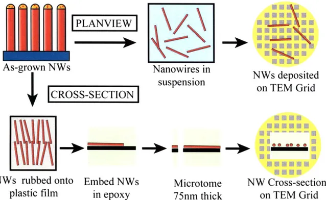
Scanning electron microscopy (SEM) required no preparation before imaging. Two types of transmission electron microscopy (TEM) were prepared: planview and cross-sectional.
Planview samples were used to investigate the properties individual nanowires as they varied across the length of the nanowire. Cross-sectional samples were used to investigate the properties of individual nanowires as they varied within the nanowire cross-section.
Planview samples were prepared, as shown in Figure 2-6, by immersing the as-grown GaAs substrates into 50-100 p.L of ethanol in a vial. The volume was set so that there was just enough ethanol to fully immerse the substrate and ensure that the nanowire density in the solution was as high as possible. The vial was immersed into a Crest 175DA ultrasonic cleaner for 10 s. To ensure that the sonication did not break the nanowires, the power of the ultrasonics was kept below 5W. To ensure that nanowires were suspended in the solution. A small droplet of solution was dropped onto a glass slide to verify the presence of nanowires in the suspension. In a Nikon Eclipse LV 100 optical microscope, nanowires appear as iridescent rods in dark field
mode at a magnification of 500 or greater. Once optical microscopy confirmed the presence of nanowires in suspension, TEM samples were prepared by depositing a 2 pL droplet of solution onto lacey carbon/formvar TEM grids (Ted Pella 1881-F), then drying in air for 5 min. To increase the density of nanowires on the TEM grid, 5 - 20 droplets of nanowire solution were typically dropped.
Cross-sectional samples were prepared using a three-step process (Figure 2-6): 1) Nanowires were transferred to a plastic coverslip by rubbing the coverslip onto the substrate, 2) The cover slip was embedded in epoxy pre-molds, and 3) The cross-sections were sliced with a diamond knife using a microtome.
Epoxy premolds were made using Eponate- 12 epoxy, purchased from Ted Pella. The epoxy was prepared by mixing proprietary Eponate 12 resin (49.9% by mass), double distilled docecenyl succinic anhydride (DDSA) (14.8% by mass), n-methyl anhydride (NMA) (32.6% by mass), and benzyldimethylamine (BDMA) (2.7% by mass) in a fume hood for five min. The epoxy was then poured into a mold so that each mold was half-filled. The molds were baked for
18 hours at 60'C, until solid.
Thermonox plastic coverslips, purchased from Ted Pella, were sliced 2 mm by 1 cm long using a pair of scissors. An as-grown substrate was affixed to a horizontal surface using double-sided carbon tape. Using a pair of tweezers, the coverslip was rubbed across the surface in a uniform direction. Multiple strokes were made to increase the density of nanowires on the coverslip. The coverslips were then placed on top of the epoxy premold, with care taken to assure that the edge of the coverslip was perfectly perpendicular to the edge of the premold. This process ensures that the nanowires, which lie in the plane of the coverslip oriented along the direction of rubbing, will be perpendicular to the diamond blade during microtomy. A second
batch of the epoxy, prepared exactly as the premold was prepared and deposited on top of the coverslips. The samples were cured again for another 18 hours at 60'C.
A r
PLANVIEW
NWs
Nanowires in
suspension*
ICROSS-SECTION
I
o.)Ws deposited
ri TEM Grid
NWs rubbed onto Embed NWs
Microtome
NW Cross-sections
plastic film
in epoxy
75nm thick
on TEM Grid
Figure 2-6: Schematic showing the preparation process for plan-view and cross-section nanowire TEM samples.
After curing the samples were trimmed to a trapezoidal shape using either a razor blade or a glass knife. The samples were sliced with a target thickness of 75 nm using a Leica UCT Microtome and a Diatome Histo diamond blade. Slices were transferred onto TEM grids by
immersing the TEM grid into the water bath. The end results are microtome slices resting on top of a TEM grid.
2.2.2
Scanning electron microscopy theory and techniques
Scanning electron microscopy (SEM) was utilized for imaging the morphology of as-grown nanowire samples. In a scanning electron microscope, an electron beam accelerated through a voltage of 0.1 - 50 kV is irradiated on a bulk samples. The beam interacts with the
sample producing secondary electrons, which are collected for imaging. SEM was conducted using a JEOL 6320FV SEM with a LaB6 thermal field emission gun. Imaging was performed at an accelerating voltage of 5 kV using a JEOL ORION charge-coupled device (CCD) camera. The only post-processing of digital images was adjustment of levels and the gamma factor. Under these conditions a maximum resolution less than 2 nm could be achieved1. To enable high resolution SEM imaging, all nanowires were grown on degenerately doped substrates.
Nanowire height could be determined from tilted SEM images by measuring the apparent height, happarent, and calculating the real height, h, from h = happarent/sin(6). The diameter
distribution and aerial density of gold nanoparticles was quantitatively determined from SEM images built-in functions of using ImageJ software.
2.2.3
Transmission Electron Microscopy
In transmission electron microscope (TEM) an electron beam is irradiated on a sample less than 500 nm thick. Since the electron beam is accelerated through a voltage of 80 -1000 kV, the impinging electrons are accelerated to a speed of 50 - 95% of the speed of light according to
special relativity [53], so the majority of electrons penetrate through the sample. However, some electrons will by scattered by the sample and spatially-dependant variations in electron scattering create the contrast that is used to form TEM images. Images in TEM are formed by a
combination of three contrast mechanisms: mass-thickness, diffraction, and phase contrast [51]. These contrast mechanisms and their applications to characterizing nanowires will be discussed. In addition, the electron beam generates X-rays, which can be used for compositional analysis in energy dispersive X-ray spectroscopy. This method will be discussed in the next section.
Bright field transmission electron microscopy
Bright-field TEM allows imaging the morphology of samples with a resolution of less than one nanometer. In this mode there are two primary contrast mechanisms: mass-thickness contrast and diffraction contrast. Mass-thickness contrast is based on the principle that the number of electrons scattered by the sample will increase with increasing mass or thickness of the sample. As a result, heavier and thicker regions of the sample will appear darker in bright field imaging.
Crystallographic defects can be imaged using diffraction contrast. Given that electrons exhibit wave-particle duality, the electron can be considered to behave like a wave with a characteristic wavelength of 0.00251 nm at 200 kV. In a perfect crystal with uniform mass and thickness the electron scattering is uniform across the sample, hence the sample appears uniform. However, a structural imperfection such as a dislocation, twin plane or stacking fault will create a diffraction plane for the electrons. The presence of this diffraction plane will create a variation of the scattering profile of the sample, which is referred to as diffraction contrast. Determining the properties of structural defects requires a more in-depth TEM analysis known as "two-beam analysis" and the Howie-Whelan equations [51].
Transmission electron microscopy was performed using a JEOL 201 OF field emission TEM operated at 200 kV and equipped with a thermal field emission gun and Gatan Orius CCD camera Model 831 SC600. The only post-processing of digital images was adjustment of levels and the gamma factor. Since nanowire growth was optimized towards eliminating structural defects, the only information required was whether a sample possessed structural defects or not. Therefore, samples were simply imaged by bright-field TEM over a variety of tilt angles and the presence of defects was noted.
High resolution transmission electron microscopy
Resolving atomic columns can be achieved using phase contrast. As the electron beam passes through a sample, interactions with the sample will shift the phases of the electrons' wave
functions. If the sample is randomly oriented, these phase shift are sporadic and average themselves out. However, if the specimen is tilted onto an axis of high symmetry such that the beam impinges parallel to the atomic columns (called a zone axis), and then the interaction of the beam with atomic columns will result in uniform phase shifts that correspond with the lattice spacing of the crystal. The net effect is an apparent image of the atomic columns. It should be noted that since there can be many sources of phase contrast in a crystal and the in microscope itself, lattice-resolved images produced by phase-contrast images require comparison with simulation for quantitative interpretation. Nevertheless, phase contrast images can provide useful qualitative information about the crystalline structure without the use of simulation.
Lattice-resolved phase contrast images, commonly referred to as high resolution (HR) images, were imaged in the same microscope and imaging conditions as bright field TEM with the following exceptions. HR images were produced by tilting a sample onto a zone axis using a double-tilted TEM sample holder. For plan view and cross-sectional samples, the <110> and <111> zone axes were used. The zone axis was found by centering the high symmetry nexus of the Kikuchi pattern.
Scanning Transmission Electron Microscopy
Scanning transmission electron microscopy (STEM) is technique complimentary to transmission electron microscopy that allows for the imaging of thin specimens by use of an electron beam transmitting through the sample. The key difference between STEM and TEM is the shape of the beam utilized in the imaging. TEM creates a parallel beam of electrons that